

Transistors
General purpose transistor
(isolated transistor and diode)
QSL10
A 2SD2674 and a RB461F are housed independently in a TSMT5 package.
zApplica tions
DC / DC converter
Motor driver
zFeatures
1) Tr : Low V
Di : Low V
CE(sat)
F
2) Small package
zStructure
Silicon epitaxial planar transistor
Schottky barrier diode
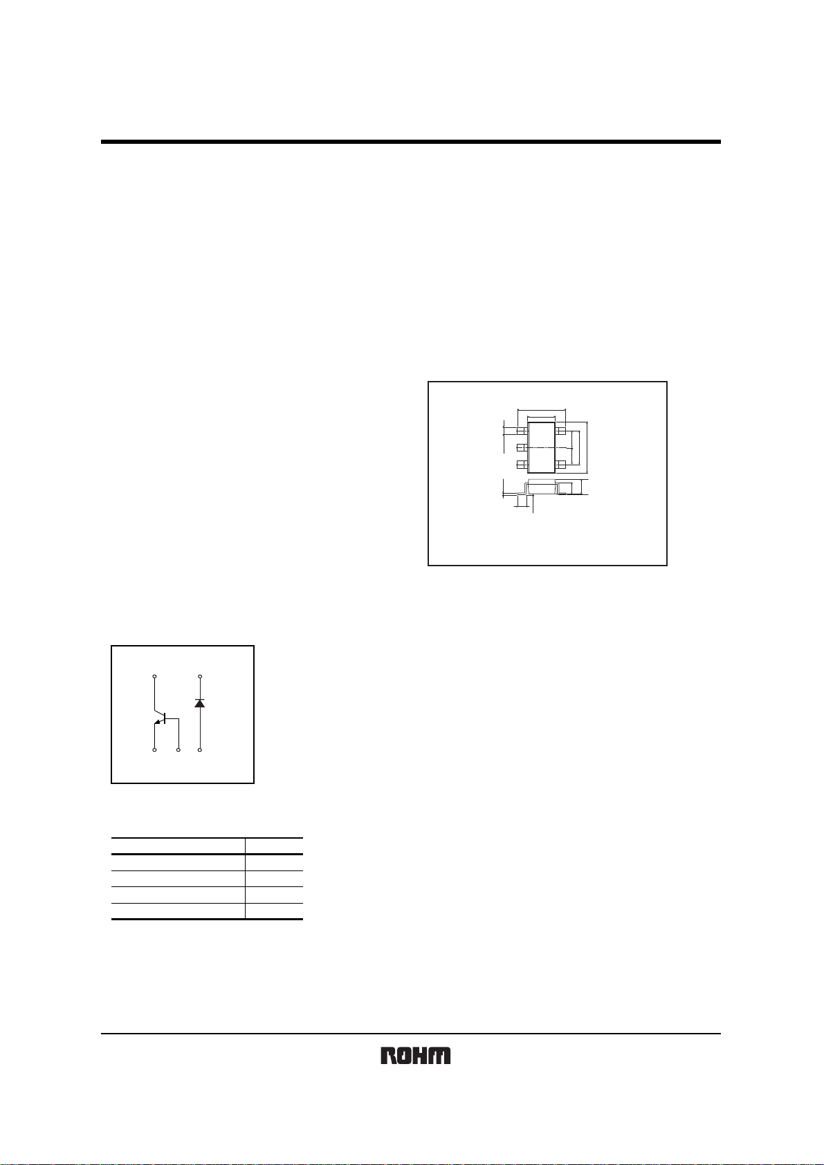
zEquivalent circuit
zExternal dimensions (Unit : mm)
QSL10
(1)
0.4
(3) (2)
0.16
0.3 to 0.6
ROHM : TSMT5
Abbreviated symbol : L10
2.8
1.6
(5)
0.95
2.9
1.9
0.95
(4)
0.85
0.7
0 to 0.1
Each lead has same dimensions
QSL10
(5) (4)
Tr1
Di2
(3)(2)(1)
zPackaging specifications
Type QSL10
Package
Marking
Code
Basic ordering unit(pieces)
TSMT5
L10
TR
3000
Rev.A 1/4
Transistors
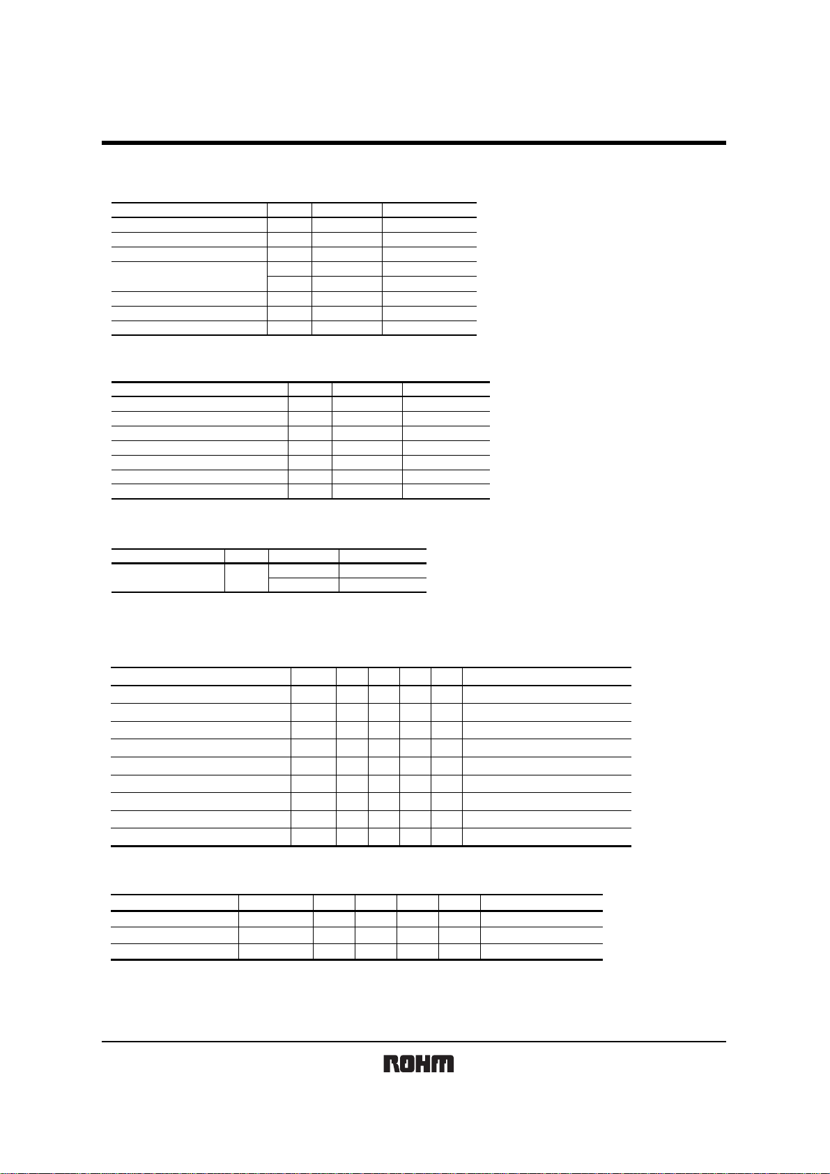
zAbsolute maximum ratings (Ta=25°C)
Tr1
P
D
Symbol
Symbol
CBO
V
V
CEO
V
EBO
I
C
I
CP
Pc
Tj
Tstg
Limits
1.25
F
V
I
R
t
rr
V
I
Tstg
0.5
BV
BV
BV
V
RM
V
R
I
F
FSM
P
D
Tj
CBO
CEO
EBO
I
CBO
I
EBO
CE(sat)
FE
h
f
T
Cob
Parameter
Collector-base voltage
Collector-emitter voltage
Emitter-base voltage
Collector current
Power dissipation
Junction temperature
Range of storage temperature
∗1 Single pulse, Pw=1ms
∗2 Mounted on a 25mm 25mm t0.8mm ceramic substrate
+
+
Di2
Parameter Symbol
Peak reverse voltage
Reverse voltage (DC)
Average rectified forward current
orward current surge peak (60HZ, 1∞)
F
Power dissipation
Junction temperature
Range of storage temperature
∗ Mounted on a 25mm 25mm t0.8mm ceramic substrate
+
+
Tr1&Di2
Parameter Symbol
Total power disipation
∗1 Each terminal mounted on a recommended land.
∗2 Mounted on a 25mm 25mm t0.8mm ceramic substrate.
+
+
zElectrical characteristics (Ta=25°C)
Tr1
Parameter Symbol Min. Typ. Max. Unit Conditions
Collector-base breakdown voltage
Collector-emitter breakdown voltage
Emitter-base breakdown voltage
Collector cutoff current
Emitter cutoff current
Collector-emitter saturation voltage
DC current gain
Transition frequency
Collector output capacitance
∗ Pulsed
Di2
Parameter
Forward voltage
Reverse current
Reverse recovery fime
/
ELEMENT
W
Unit
V
V
V
A
A
°C
°C
∗1
∗2
Limits
15
12
6
1.5
3
0.9
150
−40 to +125
Limits
25
20
700
3
0.7
125
−40 to +125
Unit
V
V
mA
A
W / ELEMENT
°C
°C
∗
Unit
W / ELEMENT
W
/
ELEMENT
1
∗
2
∗
15
−−
12
−−
6
−−
−−
−−
85 200 mV
−
270
−
400
−
12
−
Min. Typ. Max. Unit Conditions
−
− 200
−
−−
9
V
V
V
100 nA
100 nA
680
MHz
−
pF
−
490450
I
C
=10µA
C
=1mA
I
E
=10µA
I
VCB=15V
EB
=6V
V
IC/IB=500mA/25mA
− V
CE/IC
=2V/200mA
VCE=2V, I
E
=
−200mA, f=100MHz
VCB=10V, IE=0A, f=1MHz
F
mVnsI
µA
=700mA
VR=20V
F=IR
=100mA, Irr=0.1I
I
QSL10
∗
∗
R
Rev.A 2/4
 Loading...