

Data Sheet
Midium Power Transistors (30V / 3A)
QS5W1
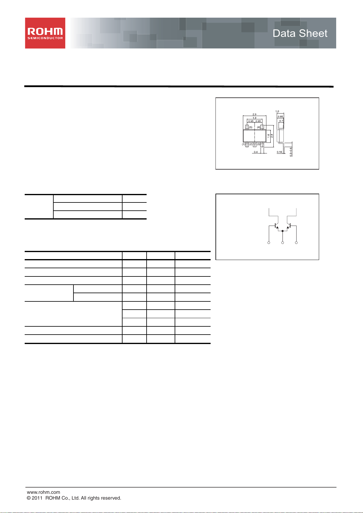
Structure Dimensions (Unit : mm)
NPN Silicon epitaxial planar transistor
Features
1) Low saturation voltage
V
= 0.4V (Max.) (IC / IB= 1A / 50mA)
CE (sat)
2) High speed switching
Applications
Low Frequency Amplifier
Driver
TSMT5
(1) Tr.1 Base
(2) Emitter
(3) Tr.2 Base
(4) Tr.2 Collector
(5) Tr.1 Collector
Abbreviated symbol : W01
Packaging specifications
Package TSMT5
Type
Code TR
Basic ordering unit (pieces) 3000
Absolute maximum ratings (Ta = 25C)
<It is the same ratings for the Tr.1 and Tr.2>
Parameter
Symbol Limits Unit
Collector-base voltage V
Collector-emitter voltage V
Emitter-base voltage
Collector current
DC I
Pulsed I
V
Power dissipation
Junction temperature T
Range of storage temperature T
*1 Pw=10ms, Single Pulse
*2 Mounted on a recommended land.
*3 Mounted on a 25 x 25 x 0.8[mm] ceramic board.
CBO
CEO
EBO
C
*1
CP
*2
P
D
P
D
P
D
j
stg
0.5 W/Total
*3
1.25 W/Total
*3
0.9 W/Element
150 C
-55 to 150 C
30 V
30 V
6V
3A
6A
Inner circuit (Unit : mm)
Tr.1 Tr.2
(1) Tr.1 Base
(2) Emitter
(3) Tr.2 Base
(4) Tr.2 Collector
(5) Tr.1 Collector
(1)
(4)(5)
(2) (3)
www.rohm.com
© 2011 ROHM Co., Ltd. All rights reserved.
1/5
2011.02 - Rev.A
www.rohm.com
© 2011 ROHM Co., Ltd. All rights reserved.
Data Sheet
QS5W1
_
Electrical characteristics (Ta=25°C)
<It is the same ratings for the Tr.1 and Tr.2>
Collector-emitter breakdown voltage
Collector-base breakdown voltage
Emitter-base breakdown voltage
Collector cut-off current
Emitter cut-off current
Collector-emitter staturation voltage
DC current gain
Transition frequency
Turn-on time
Storage time
Fall time
*1 Pulsed
*2 See switching time test circuit
Symbol Min. Typ. Max. Unit
BV
BV
BV
I
I
V
CE(sat)
CBO
EBO
h
f
C
t
t
stg
t
CEO
CBO
EBO
FE
T
ob
on
f
30 - - V
30 - - V
6--V
--1
--1
*1
- 200 400 mV
200 - 500 -
*1
-
-16Collector output capacitance
-25-ns
*2
- 300 - ns
*2
-20-ns
*2
-
A
A
MHz270 -
pF
ConditionsParameter
= 1mA
I
C
= 100μA
I
C
= 100μA
I
E
= 30V
V
CB
= 4V
V
EB
= 1A, IB= 50mA
I
C
= 2V, IC= 500mA
V
CE
= 10V
V
CE
I
=-100mA, f=100MHz
E
= 10V, IE=0A
V
CB
f=1MHz
I
= 1.5A, IB1= 150mA,
C
I
=-150mA, V
B2
CC
~
12V
2/5
2011.02 - Rev.A

www.rohm.com
© 2011 ROHM Co., Ltd. All rights reserved.
Data Sheet
QS5W1
Electrical characteristic curves (Ta=25C)
0.0
0.1
0.2
0.3
0.4
0.5
0 0.5 1 1.5 2
COLLECTOR CURRENT : I
C
[A]
COLECTOR TO EMITTER VOLTAGE :VCE[V]
Fig.1 Typical Output Characteristics
2mA
1.5mA
1.0mA
IB=0.5mA
5mA
Ta=25°C
2.5mA
10
100
1000
1 10 100 1000 10000
DC CURRENT GAIN : h
FE
COLLECTOR CURRENT : IC[mA]
Fig.2 DC Current Gain vs. Collector Current ( I )
VCE=5V
2V
Ta=25°C
10
100
1000
1 10 100 1000 10000
DC CURRENT GAIN : h
FE
COLLECTOR CURRENT : IC[mA]
Fig3. DC Current Gain vs. Collector Current ( II )
VCE=2V
Ta=125°C
75°C
25°C
-40°C
0.001
0.01
0.1
1
1 10 100 1000 10000
COLLECTOR SATURATION VOLTAGE : V
CE
(sat)[V]
COLLECTOR CURRENT : IC[mA]
Fig.4 Collector-Emitter Saturation Voltage vs. Collector Current ( I )
Ta=25°C
Pulsed
IC/IB=50
20
10
0.001
0.01
0.1
1
1 10 100 1000 10000
COLLECTOR SATURATION VOLTAGE : V
CE
(sat)[V]
COLLECTOR CURRENT : IC[mA]
Fig.5 Collector-Emitter Saturation Voltage vs. Collector Current ( II )
IC/IB=20
Pulsed
Ta=125°C
75°C
25°C
-40°C
1
10
100
1000
10000
0 0.2 0.4 0.6 0.8 1 1.2 1.4
COLLECTOR CURRENT : I
C
[mA]
BASE TO EMITTER VOLTAGE : VBE[V]
VCE=2V
Fig.6 Ground Emitter Propagation Characteristics
Ta=125°C
75°C
25°C
-40°C
3/5
2011.02 - Rev.A

www.rohm.com
© 2011 ROHM Co., Ltd. All rights reserved.
Data Sheet
QS5W1
1
10
100
1000
0.1 1 10 100
COLLECTOR OUTPUT CAPACITANCE : Cob(pF)
EMITTER INPUT CAPACITANCE : Cib(pF)
COLLECTOR - BASE VOLTAGE : VCB (V)
EMITTER - BASE VOLTAGE : VEB (V)
Fig.7 Emitter Input Capacitance vs. Emitter-Base Voltage
Collector Output Capacitance vs. Collector-Base Voltage
Ta=25°C
f=1MHz
I
E
=0A
IC=0A
Cob
Cib
10
100
1000
-10 -100 -1000
TRANSITION FREQUENCY : f
T
[MHz]
EMITTER CURRENT : IE[mA]
Ta=25°C
VCE=10V
Pulsed
Fig.8 Gain Bandwidth Product vs. Emitter Current
0.001
0.01
0.1
1
10
0.1 1 10 100
COLLECTOR CURRENT : I
C
[A]
COLLECTOR TO EMITTER VOLTAGE : VCE[V]
Fig.9 Safe Operating Area
DC
(Mounted on a recommended land)
10ms
1ms
100ms
Ta=25°C
When one element operated
Single non repetitive pulse
4/5
2011.02 - Rev.A

www.rohm.com
© 2011 ROHM Co., Ltd. All rights reserved.
Data Sheet
QS5W1
w
f
_~_
Switching time test circuit
V
P
BASE CURENT WAVEFORM
RL=8.2Ω
I
IN
Pw 50μs
DUTY CYCLE≦1%
B1
I
C
I
B2
I
B1
VCC12V
~
COLLECTOR CURRENT
WAVEFORM
90%
10%
I
B2
t
on
t
t
stg
I
C
5/5
2011.02 - Rev.A

Notes
Notice
www.rohm.com
© 2011 ROHM Co., Ltd. All rights reserved.
Thank you for your accessing to ROHM product informations.
More detail product informations and catalogs are available, please contact us.
ROHM Customer Support System
http://www.rohm.com/contact/
R1120A
 Loading...