

查询PTZ3.9B供应商
PTZ3.6B
Diodes
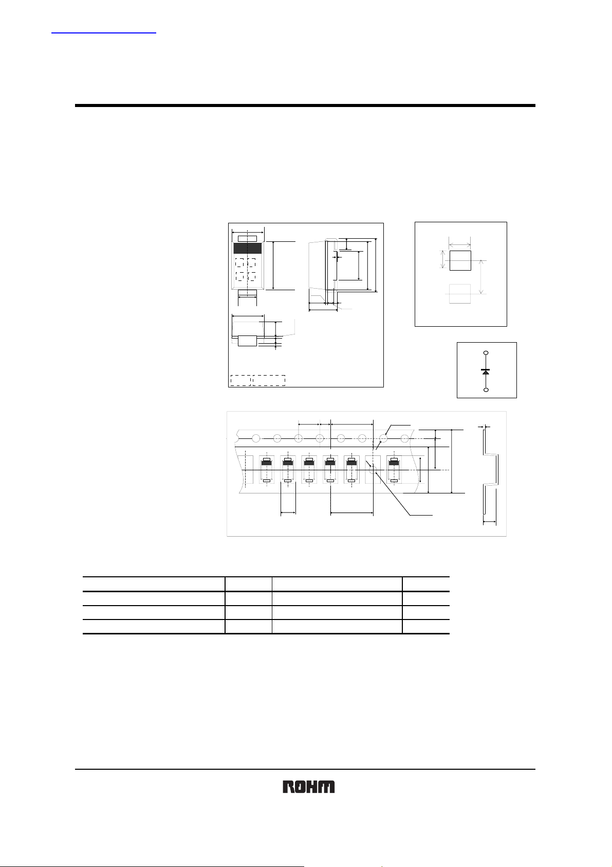
Zener diode
PTZ3.6B
zApplicat ions zExternal dimensions (Unit : mm) zLand size figure (Unit : mm)
Voltage regulation
zFeatures
1) Small power mold type. (PMDS)
2) High ESD tolerance
zConstruction
Silicon epitaxial planar zStructure
zT aping dime nsions (Unit : mm)
zAbsolute maximum ratings (Ta=25°C)
ower dissipation
P
unction temperature
J
torage temperature
S
Param eter
2.6±0.2
1.2±0.3
45
① ②
1.5±0.2
2.6±0.03
RO HM : PMD S
JEDEC : SO D-106
①
4.5±0.03
②
0.2±0.01
0.2
1.030.25 0.5
Manu factu re Date
4.0±0.1
Sym bol Unit
Pm
Tj
Ts tg
0.1±0.02
0.1
1.03
0.25
0.5
2.0±0.2
2.0±0.05
8.0±0.1
8.0±0.12.9±0.1
Limits
1000
150
-5 5 to + 150
2±0.05
4.5±0.03
5.0±0.3
PMDS
φ1.55±0.1
0
φ1.55±0.05
℃
℃
2.0
2.0
4.2
0.3±0.1
1.75±0.05
5.5±0.05
12.0±0.3
9.5±0.1
5.3±0.1
2.4±0.1
W
Rev.B 1/4
PTZ3.6B
Diodes
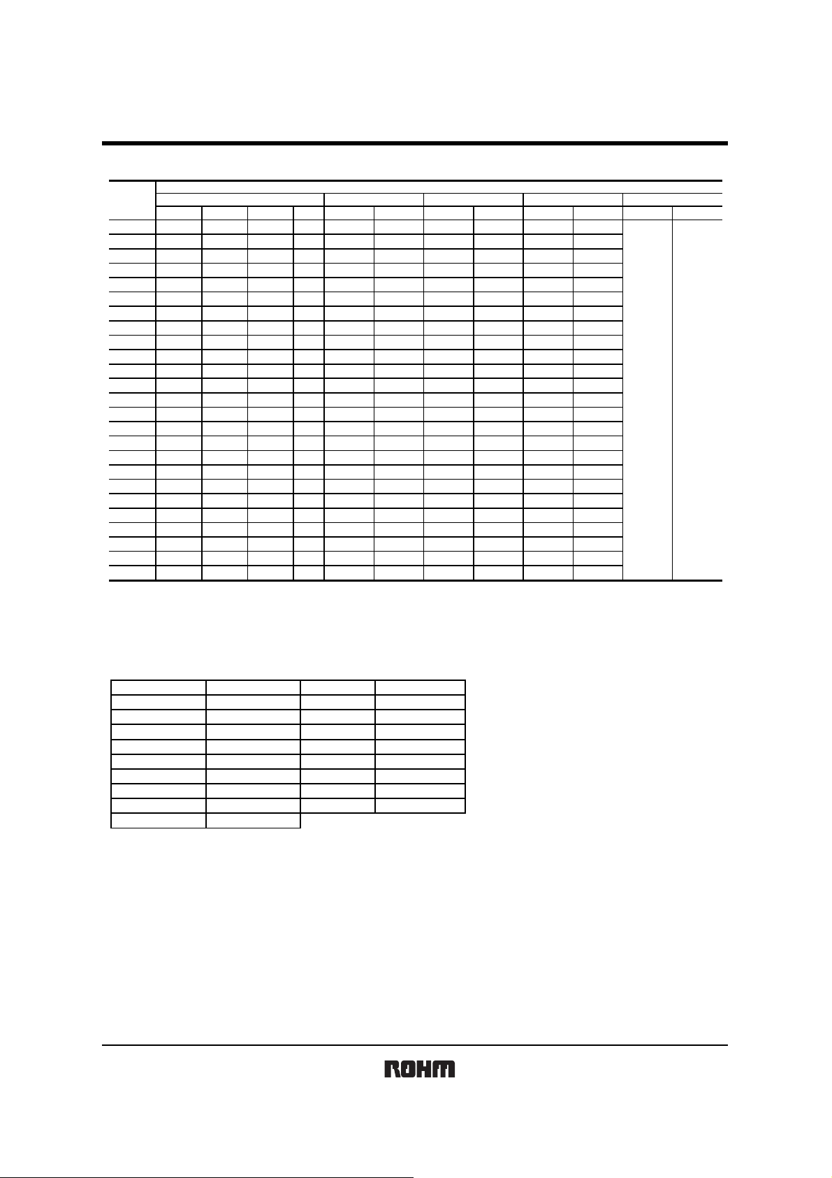
zElectrical characteristics (Ta=25°C)
PTZ 3.6B 3.600 3.813 4.000 40 15 40 60
PTZ 3.9B 3.900 4.136 4.400 40 15 40 40
PTZ 4.3B
PTZ 4.7B
PTZ 5.1B
PTZ 5.6B
PTZ 6.2B
PTZ 6.8B
PTZ 7.5B
PTZ 8.2B
PTZ 9.1B
PTZ 10B
PTZ 11B
PTZ 12B
PTZ 13B
PTZ 15B
PTZ 16B
PTZ 18B
PTZ 20B
PTZ 22B
PTZ 24B
PTZ 27B
PTZ 30B
PTZ 33B
PTZ 36B 36.000 39.240 40.000 10 20 10 10 27.0 37.0 10
1.The Zener voltage(Vz) is measured 40ms after power is supplied.
2.The operating resistances(Zz、Zzk) are measured by superimposing a minute alternating current on the regulated current(Iz).
zMarking (TYPE NO.)
TYP.
MIN.
4.300 4.572 4.800
4.700 4.924 5.200
5.100 5.368 5.700
5.600 5.856 6.300
6.200 6.509 7.000
6.800 7.280 7.700
7.500 7.889 8.400
8.200 8.655 9.300
9.100 9.747 10.200
10.000 10.310 11.200
11.000 11.510 12.300
12.000 12.500 13.500
13.300 13.820 15.000
14.700 15.350 16.500
16.200 16.860 18.300
18.000 19.000 20.300
20.000
22.000
24.000 25.310 27.600
27.000 28.700 30.800
30.000 31.570 34.000
33.000 34.950 37.000
TYP.
PTZ 3.6B
PTZ 3.9B
PTZ 4.3B
PTZ 4.7B
PTZ 5.1B
PTZ 5.6B
PTZ 6.2B
PTZ 6.8B
PTZ 7.5B
Zener voltage : Vz(V)
TYP.
20.820
23.850
MAX. Iz(mA) Max. Iz(mA) MAX. VR(V)
22.400
24.500
TYPE NO.
3.6B
3.9B
4.3B
4.7B
5.1B
5.6B
6.2B
6.8B
7.5B
Operating resis tance : Zz(Ω)
40
15
40
10
40
40
40
40
40
40
40
40
20
20
20
20
20
20
8
8
6
6
4
4
6
6
8
8
10
10
12
12
20 14 20
10 14 10
10 16
10 16
10 18
10 18
TYP.
PTZ 8.2B
PTZ 9.1B
PTZ 10B
PTZ 11B
PTZ 12B
PTZ 13B
PTZ 15B
PTZ 16B
Symbol
Reverse current : IR(μA)
40
40
40
40
40
40
40
40
40
40
20
20
20
20
20
20
10 10 19.0 21.6
10 10 21.0 24.6
10 10 23.0 27.5
10 10 25.0 30.8
TYPE NO.
20 1.0 -2.1
20 1.0 -1.7
20 1.5 -0.6
20 2.5 1.4
20 3.0 2.5
20 3.5 3.2
20 4.0 4.2
20 5.0 5.0
20 6.0 5.9
10 7.0 6.9
10 8.0 7.9
10 9.0 8.7
10 10.0 10.1
10 11.0 11.8
10 12.0 13.3
10 13.0 15.0
10
10
Temperature coefficiency :
TYP.
1.0 -2.8
1.0 -2.4
15.0 17.4 20
17.0 19.4 10
8.2B
9.1B
10B
11B
12B
13B
15B
16B
*γz(mV/℃)
Iz(mA) MIN.
ESD Break down voltage : ESD(kV)
40
40
40
40
40
40
40
40
40
40
40
40
20
20
20
20
20
20
10
10
10
10
30kV
Test Condition
C=150pF
Ω
R=330
forward
and
reverse :
10 times
Rev.B 2/4

Diodes
zElectrical characteristic curves (Ta=25°C)
100
10
ZENER C URREN T:Iz(mA)
0.1
0.01
0.001
5.1
4.7
4.3
3.9
3.6
1
0 5 10 15 20 25 30 35 40 45
20
1615131211109.18.27.55.6 6.86.2
18
ZENER V OLTAGE:Vz(V)
Vz-Iz CHARACTERISTICS
22
PTZ3.6B
24
30
27
33
36
1200
1000
800
600
400
POWER DISSIPATION:Pd(W)
200
0
0 255075100125150
AMBIENT TEMPERATURE:Ta(℃)
Pd-Ta CHARACTERISTICS
0.12
0.1
0.08
0.06
0.04
0.02
0
-0.02
-0.04
TEMP.COEFFICIENCE:γz(%/℃)
-0.06
-0.08
010203040
TIME:t( ms)
IFSM- t CHA RACT ERISTICS
10000
PRSM
1000
100
POWER:PRSM(W)
10
REVERSE SURGE MAXIMUM
1
0.001 0.01 0.1 1 10 100
TIME: t(m s)
PRSM-TIME CHARACTERISTICS
40
35
30
25
20
15
10
5
0
-5
TRA NSIENT
TEMP.COEFFICIENCE:γz(mV/℃)
Mounted on epoxy board
1000
IM=10mA IF=0.5A
100
10
1
THAERMAL IMPEDANCE:Rth (℃/W)
0.1
0.001 0.1 10 1000
time
1ms
300us
TIME:t( s)
Rth-t CHARACTERISTICS
t
Rth(j-a)
Rth(j-c)
Rev.B 3/4

Diodes
<PTZ3.6B>
100
10
1
0.1
ZENER C URREN T:Iz(mA)
0.01
0.001
01234
Ta=150℃
ZENER V OLTAGE:Vz(V )
Vz-Iz CHARACTERISTICS
Ta=75℃
Ta=125℃
Ta=-25℃
Ta=25℃
1000
100
10
1
0.1
0.01
REVERSE CURRENT:IR(nA)
0.001
0.0001
0 0.1 0.2 0.3 0.4 0.5 0.6 0.7 0.8 0.9 1
REVERSE VOLTAGE:VR(V)
VR-IR CHARACTERISTICS
Ta=75℃
Ta=25℃
Ta=-25℃
Ta=150℃
Ta=125℃
100
10
TERM INAL S:Ct(pF )
CAPACITANCE BETWEEN
1
0 0.2 0.4 0.6 0.8 1
REVERSE VOLTAGE:VR(V)
VR-Ct CHARACTERISTICS
PTZ3.6B
f=1MHz
f=1MHz
4
3.9
3.8
3.7
ZENER V OLTAGE:Vz(V)
3.6
3.5
10000
1000
100
DYNAMIC IMPEDANCE:Zz(Ω)
10
0.1 1 10
AVE:3.813V
Vz DISPERSION MAP
ZENER CURRENT:Iz(mA)
Zz-Iz CHA RACTERISTICS
Ta=25℃
IZ=40mA
n=30pcs
1
0.9
0.8
0.7
0.6
0.5
0.4
0.3
0.2
REVERSE CURRENT:IR(nA)
0.1
0
30
25
20
15
ELECTROSTATIC
10
DD ISCHA RGE TEST E SD(KV )
5
0
AVE:0.094nA
IR DISPE RSION MAP
No break at 30kV
C=200pF
R=0Ω
ESD DISPERSION MA P
C=100pF
R=1.5kΩ
Ta=25℃
VR=1.0V
n=30pcs
C=150pF
R=330Ω
60
59
58
57
56
55
54
53
TERM INA LS:Ct(pF)
52
CAPACITANCE BETWEEN
51
50
AVE:55.43pF
Ct DISPERSION MAP
Ta=25℃
VR=0V
f=1MH z
n=10pcs
Rev.B 4/4

Appendix
No technical content pages of this document may be reproduced in any form or transmitted by any
means without prior permission of ROHM CO.,LTD.
The contents described herein are subject to change without notice. The specifications for the
product described in this document are for reference only. Upon actual use, therefore, please request
that specifications to be separately delivered.
Application circuit diagrams and circuit constants contained herein are shown as examples of standard
use and operation. Please pay careful attention to the peripheral conditions when designing circuits
and deciding upon circuit constants in the set.
Any data, including, but not limited to application circuit diagrams information, described herein
are intended only as illustrations of such devices and not as the specifications for such devices. ROHM
CO.,LTD. disclaims any warranty that any use of such devices shall be free from infringement of any
third party's intellectual property rights or other proprietary rights, and further, assumes no liability of
whatsoever nature in the event of any such infringement, or arising from or connected with or related
to the use of such devices.
Upon the sale of any such devices, other than for buyer's right to use such devices itself, resell or
otherwise dispose of the same, no express or implied right or license to practice or commercially
exploit any intellectual property rights or other proprietary rights owned or controlled by
ROHM CO., LTD. is granted to any such buyer.
Products listed in this document are no antiradiation design.
Notes
The products listed in this document are designed to be used with ordinary electronic equipment or devices
(such as audio visual equipment, office-automation equipment, communications devices, electrical
appliances and electronic toys).
Should you intend to use these products with equipment or devices which require an extremely high level of
reliability and the malfunction of with would directly endanger human life (such as medical instruments,
transportation equipment, aerospace machinery, nuclear-reactor controllers, fuel controllers and other
safety devices), please be sure to consult with our sales representative in advance.
About Export Control Order in Japan
Products described herein are the objects of controlled goods in Annex 1 (Item 16) of Export Trade Control
Order in Japan.
In case of export from Japan, please confirm if it applies to "objective" criteria or an "informed" (by MITI clause)
on the basis of "catch all controls for Non-Proliferation of Weapons of Mass Destruction.
Appendix1-Rev1.1
 Loading...