

Contact Image Sensor Heads for narrow-width scanners
LSH2004-AA10A
Equipped with the sensor chips that have built-in analog memory, this compact color Contact Image Sensor Heads is suitable
for any scanning applications that require rapid scanning of widths of up to A6. It best fits into the photo graphic applications.
Applications
Check readers, card scanners, and a variety of other image input devices.
Features
1) By integrating the signal amplifier on the sensor chip, external noise is shut out. Additionally, newly developed analog
memory circuit and realizes high speed scanning.
2) The LED light source is mounted on the same substrate as the sensor chip which makes it possible to package the
device with lighter weight and an extremely small size.
3) With the proprietary prism(reflectors), the output signal is maintained uniformly.
4) The ceramic substrate is used for excellent dimensional accuracy and thermal stability.
Variation and maximize the image re-productivity.
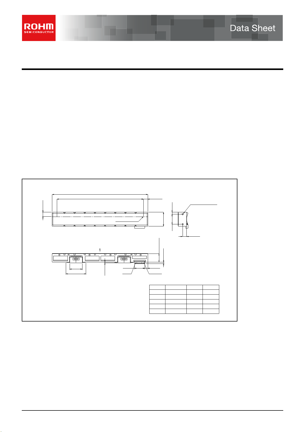
Dimensions (Unit : mm)
5.5 0.3
±
±
119.5 0.3
108(Effective Reading Width:104)
±
0.3
5.5
2.5
±
φ
2 0.05
Depth1
C
L
A
15.5 1
±
±
25 1
Note) Deflection at the top of glass : 0 to 0.25
Projection to platen is positive
Socket Housing : IL-Z-7S-S125C3(JAE)
Socket Contact : IL-Z-C3-A-15000(JAE)
No.1 Pixel
Max. 1.5
(10.4)
No.7
(3.8)
No.1
Pin No. Pin No.Signal Signal
No.1
No.2
No.3
No.4
No.5
0.25
±
17.5
±
Max.2
10.36 0.4
12.5 0.05
±
Ao
GND
SI
CLK
V
DD
±
5 0.1
No.6
No.7
GLED
VLED
www.rohm.com
1/3
c
○
2011 ROHM Co., Ltd. All rights reserved.
2011.03 - Rev.B
Data Sheet LSH2004-AA10A
Characteristics
Effective scanning width
Primary scan dot density
Total dot number
Power supply voltage
Scanning speed
Clock frequency
Maximum dynamic range
Minimum dynamic range
Dark output
Operating temperature
Analogue signals are produced output at double rate of clock frequency.
Parameter
Symbol Typ. Unit
−
−
−
DD
V
SLT
CLK
VRMax.
VRMin.
Vod
−
Pin assignments
No.
1
2
3
4
5
6
7
Circuit
Ao
GND
Sl
CLK
DD
V
G-LED
V-LED
I / O
Analog output
O
Ground
I
Serial-in
I
Clock
I
I
Power supply
I
LED ground
I
LED power supply
Functions
Timing chart
(a) CLK Timing Chart
CLK
twCLK
1/fCLK
twCLK
104
203
864
5
0.4
1.25
0.75
0.375
1.7±0.2
5 to 45
trCLK tfCLK
90%
50%
10%
mm
dpi
dots
V
ms / line
MHz
V
V
V
°C
∗
90%
50%
10%
SP
Ao
tSETUP
tHOLD
t pd1
ts
1pixel 2pixel
www.rohm.com
2/3
c
○
2011 ROHM Co., Ltd. All rights reserved.
2011.03 - Rev.B
(b) Data Output Timing Chart
After turning on the SI pulse, the analog output shape starts from the setting up point of 27 clock pulse.
1 2 3 4 26 27 28 29
CLK
SI
Ao
Data Sheet LSH2004-AA10A
Note) Output blank part cannot be used as the analog output standard level.
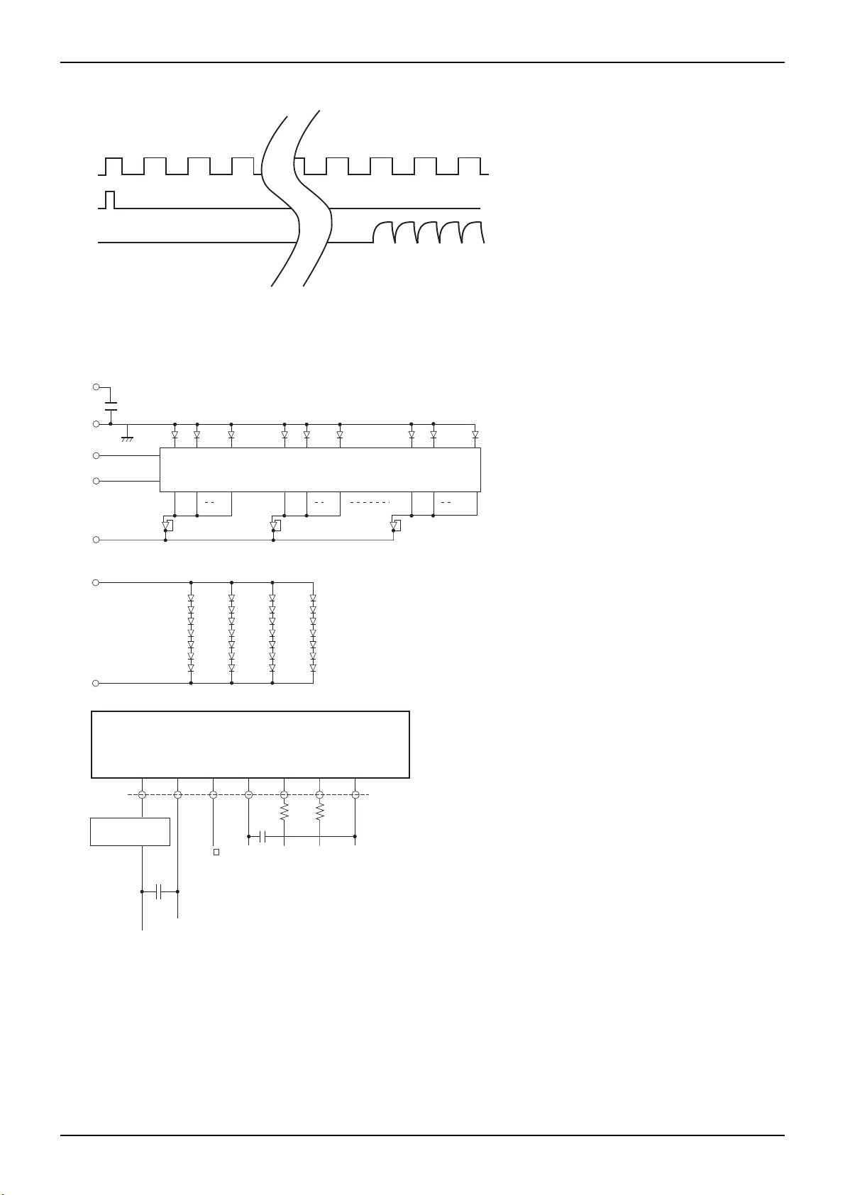
Inner circuit
V
DD
GND
SP
CLK
V
LED
G
LED
Ao
0.1μF x 3
1
ANALOG MEMORY CIRCUIT
864
6715342
R2 R1
Current adjust
Circuit
A V
C1
DD
SP CKL GND
C3
VLED
C1=47μF
∗
R1, R2=500
LED GND
C3=100μF
∗Please adjust the value of resistance to fit your interface circuit.
www.rohm.com
3/3
c
○
2011 ROHM Co., Ltd. All rights reserved.
2011.03 - Rev.B

Notes
Notice
www.rohm.com
© 2011 ROHM Co., Ltd. All rights reserved.
Thank you for your accessing to ROHM product informations.
More detail product informations and catalogs are available, please contact us.
ROHM Customer Support System
http://www.rohm.com/contact/
R1120A
 Loading...