


KF3003-GL50A
Printheads
Thick Film Thermal Printhead (300DPI)
KF3003-GL50A
KF3003-GL50A is developing type of GL40 series which are developed mainly for label printers.
We have adopted low coefficient of abrasion and conductive protection coat to GL40 series which are possible for high
speed and good printing quality.
That is KF3003-GL50A which is 24V standard thick film thermal print head with high speed, high quality of printing, high
durability, long life, and strong resistance to abration.
Applications
!!!!
High speed label printer
Food label printer
High speed ticket printer
High speed terminal printer
Features
!!!!
1) Perform 150km life time adopting new protective coat.
(Perform three times life time by coefficient of abrasion which is about is about 1/10 of current mass-producing coat.)
2) Build in thermal high speeded heater and perform high printing 6 IPS. (150mm / s)
3) Available for thermal transfer printing by adopting specific partial glaze.
4) Use the structure of thermal G-series which had good actual results. And these good results will guarantee high
reliability of GL-series.
5) Line-up for 2 and 4 inches.
External dimensions
!!!!
(4.844)
(3)
Max.36
Max.45
#2
(Units : mm)
91
81.312(Effetive Print Width)
DOT #960
#20
DOT #1
TYPE OF PRINTHEAD
6.1±0.4
(5)
20
φ
#6
#1
Max.5.5
Max.10
φ3H10 Length 4
(Effective Depth 3)
(20.8)
25±0.5
3-M3(Effective Depth 3)
40±0.3
60.5±0.3
φ3H10
(Effective Depth 3)
20.656±0.2
20±0.3
DOT #960
20.5±0.3
7.3±0.3
15.3±0.3
17.8±0.2
#1
HIROSE HIF3FC-20PA-2.54DS
#19
JST B6PS-VH
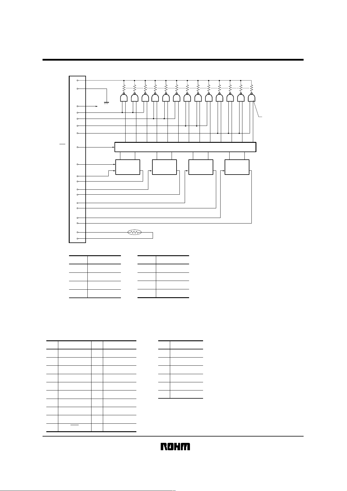
Printheads
Equivalent circuit
!!!!
VH
GND
KF3003-GL50A
DOT #960 DOT #1
V
STB4
STB3
STB2
STB1
LAT
CLK
DI4
DO4
DI3
DO3
DI2
DO2
DI1
DO1
TM
TM
DD
SHIFT
REGISTER
CONNECTOR
DI No.
DI1 1~256 1~256
DI2
DI3
DI4
DOT No.
257~512
513~768
769~960
STB No.
STB1
STB2
STB3
STB4
12 8 5 4 2
REGISTER
THERMISTOR
30kΩ B : 3950
LATCH REGISTER
SHIFT
915 14 13
SHIFT
REGISTER
SHIFT
REGISTER
DOT No.
257~512
513~768
769~960
1
64 OUTPUT EACH
Pin configuration
!!!!
CONNECTOR A CONNECTOR B
No.
10
Circuit
1
2
3
4
5
6
7
8
9
GND
V
DD
GND
V
DD
STB4
CLK
DI4
DO4
STB3
LAT
No.
11
12
13
14
15
16
17
18
19
20
Circuit
TM
TM
DI3
DO3
DI2
DO2
STB2
STB1
DI1
DO1
Fig. 1
No.
Circuit
1
2
3
4
5
6
VH
VH
VH
GND
GND
GND

Printheads
Timing chart
!!!!
CLOCK (CLK)
KF3003-GL50A
Min.30ns
Min.30ns
DATA IN (DI)
"High" : BLACK
"Low" : WHITE
DATA OUT (DO)
"High" : BLACK
"Low" : WHITE
LATCH (LAT)
"High" : HOLD
"Low" : THROUGH
STROBE (STB)
DRIVER OUT
Characteristics
!!!!
Parameter
Effective printing width
Dot pitch
Total dot number
Average resistance value
Applied voltage
Applied power
Print cycle
Pulse width
Maximum number of dots energized simultaneously
Maximum clock frequency
Maximum roller diameter
Running life / pulse life
Operating temperature
Min.10ns
Max.120ns
Min.50nsMin.200ns
Min.100ns
Fig.2
Min.300ns
Max.10µs
Symbol Typ. Unit
-
-
-
Rave
V
P
SLT
ON
T
-
-
-
-
-
H
O
81.31
0.0847
960
1250
24
0.42
0.83
0.284
960
8
φ20.0
150 / 1×10
5~45
8
mm
mm
dots
Ω
V
W / dot
ms
ms
dots
MHz
mm
km / pulses
˚C
Max.10µs

Printheads
Data sheet
!!!!
0.40
0.35
0.30
0.25
0.20
0.15
ENERGY : (mJ / dot)
0.10
0.50
0
0 2 2.50.5 1 1.5
SLT : (ms / line)
Fig.3 Maximum energy curve
1.6
1.4
1.2
1.0
0.8
O.D
0.6
0.4
0.2
0
0 0.02 0.04 0.06 0.08 0.1 0.12 0.14 0.16 0.18
ENERGY : (mj / dot)
Fig.4 Representative density curve
SPEED : 4IPS
KF3003-GL50A
180
160
140
120
kΩ)
100
80
60
RESISTANCE : (
40
20
0
−20 −10 10 30 50 700204060
TEMPERATURE : (˚C)
Fig.5 Thermistor curve
 Loading...