

Page 1
KD2002-DF10A
Printheads
Compact medium speed thick film
thermal printhead (8 dots / mm)
KD2002-DF10A
Using its expertise in LSI technolo gy , R OHM has developed new high density driver ch ips for use in the KD2002-DF10A .
Capable of being employed for bot h thermal and therm al transfer pr inting, with a print speed of 25 0mm/s, the resulti ng
print heads are the fastest in their c lass. This high-speed and high-density printing answers the needs of POS, ATM,
KIOSK and ticket printing devices, which are increasingly being called upon to produce graphical output.
zApplications
POS printers
ATM printers
KIOSK printers
Ticket printers
zFeatures
1) The use of a special partial glaze and the latest heating elemen t structure, along w ith new high-de nsity driver chip s that
can accept big current, has allowed ROHM to achieve print speeds of 250mm/s with using thermal history control, the
fastest in its class.
2) Standard printheads in the line up are capable of 203 or 300 dpi. They achieve the high resolution needed for graphics
and other complex print patterns.
3) One rank resistance value of 650Ω ± 3% eliminates the inconvenience of rank selection.
4) The required driving voltage of 3.15 to 5.25V allows wide range of power supply voltage setting. This also allows
multiple choice of electronic co mponents fo r printers.
5) 2-inch, 3-inch and 4-inch series are available.
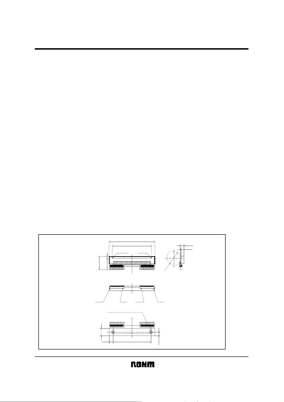
zDimensions (Unit : mm)
DOT #448
65
DOT #1
55±0.2
56 (EFFECTIVE PRINT WIDTH)
Max.20
2.6±0.1
NO.15 NO.1 NO.1NO.15
CONNECTOR B CONNECTOR A
2−M3 (EFFECTIVE DEPTH 3)
(10.2)
5±0.2
φ20.0
5.1±0.1
5.1±0.4
4±0.2
Rev.A 1/4
Page 2
KD2002-DF10A
r
Printheads
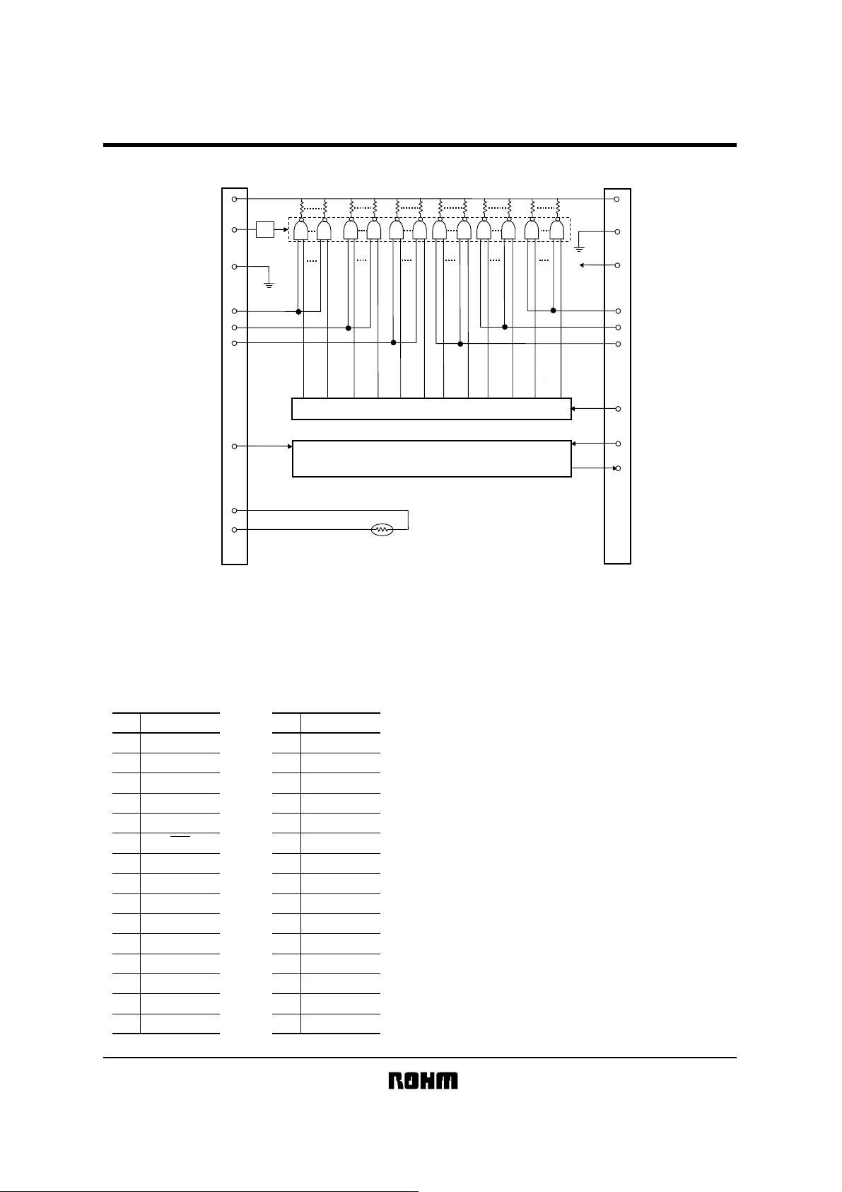
zEquivalent circuit
Dot#448
V
H
V
SF
L/S
448 385
384 321 320 257 192 129
256 193
GND
STB6
STB5
STB4
Latc h Reg ist er
DI
Shift Register
TM
TM
VH: Print Voltage
Connector B
VSF: Driver Output Voltage
STB: Strobe (High active)
/LAT: Latch
CLK: Clock
DI: Data in
DO: Data out
GND: Ground
TM: Thermisto
Thermisto r
30KΩ B: 3950K
VSF : Usually VSF and VH are connected.
When measuring R value of Heat-
element, V
separated (Page4, 7.(4)).
and VH should be
SF
zPin assignments
CONNECTOR A CONNECTOR B
No.
Circuit
1VH
2
3
4
5
6
7
8
9
10
11
12
13
14
15
VH
VH
VH
DO
LAT
CLK
V
DD
STB1
STB2
STB3
GND
GND
GND
GND
No.
10
11
12
13
14
15
Circuit
1 GND
2
3
4
5
6
7
8
9
GND
GND
GND
GND
TM
TM
STB4
STB5
STB6
DI
VSF
VH
VH
VH
Rev.A 2/4
Dot#1
1
128
Connector A
V
GND
V
DD
STB1
STB2
STB3
/LAT
CLK
DO
H
Page 3

Printheads
zTiming chart
CLK(Clock)
tsetup DI thold DI
DI(Data in)
"High" :Black
"Low" :White
DO(Data out)
"High" :Black
"Low" :White
/LAT(Latch)
"High" : Hold
"Low":Through
STB(Strobe)
DRIVER OUT
*If delay time for Driver Out can not be secured enough, there is a poss ibility that VH would fluctuate
greatly. Please design the circuit so that V
zCharacteristics
Parameter
Effective printing width
Dot pitch
Total dot number
Average resistance value
Applied voltage
Applied power
Print cycle
Pulse width
Maximum number of dots energized simultaneously
Maximum clock frequency
Maximum roller diameter
Running life / pulse life
Operating temperature
tw CLK
td DO
tsetup LAT
thold LAT
tw LAT tsetup STB
tdo tdo
does not exceed peak voltage (Vp).
H
Symbol Typical Unit
−
−
−
Rave
H
V
P
O
SLT
ON
T
−
−
−
−
−
56.0
0.125
448
650
24
0.79
0.5
0.19
448
16
φ20.0
50/5×10
5 to 45
7
mm
mm
dots
Ω
V
W/dot
ms
ms
dots
MHz
mm
km/pulses
°C
KD2002-DF10A
min.10µsec*
Rev.A 3/4
Page 4

Printheads
zElectrical characteristic curves
0.8
0.7
0.6
0.5
mJ/dot)
0.4
0.3
ENERGY (
0.2
0.1
0
012345
SCANNING LINE TIME (
Fig.3 Adaptive speed chart
180
160
140
120
100
80
60
RESISTANCE : (kΩ)
40
20
0
−20 −10 10 30 50 700204060
Fig.6 Thermistor curve
Paper : KF50-HDA (OJI)
ms/line)
TEMPERATURE : (°C)
1.8
1.6
1.4
1.2
1.0
0.8
0.6
OPTICAL DENSITY
0.4
0.2
0.0
0.00 0.05 0.10 0.15 0.20 0.25 0.30
ENERGY (
SLT : 1.25ms/line
mJ/dot)
Fig.4 Representative density curve
KD2002-DF10A
0.8
0.7
0.6
0.5
mJ/dot)
0.4
0.3
ENERGY (
0.2
0.1
0
012345
SCANNING LINE TIME (
Fig.5 Maximum energy curve
ms/line)
Rev.A 4/4
Page 5

Appendix
Notes
No technical content pages of this document may be reproduced in any form or transmitted by any
means without prior permission of ROHM CO.,LTD.
The contents described herein are subject to change without notice. The specifications for the
product described in this document are for reference only. Upon actual use, therefore, please request
that specifications to be separately delivered.
Application circuit diagrams and circuit constants contained herein are shown as examples of standard
use and operation. Please pay careful attention to the peripheral conditions when designing circuits
and deciding upon circuit constants in the set.
Any data, including, but not limited to application circuit diagrams information, described herein
are intended only as illustrations of such devices and not as the specifications for such devices. ROHM
CO.,LTD. disclaims any warranty that any use of such devices shall be free from infringement of any
third party's intellectual property rights or other proprietary rights, and further, assumes no liability of
whatsoever nature in the event of any such infringement, or arising from or connected with or related
to the use of such devices.
Upon the sale of any such devices, other than for buyer's right to use such devices itself, resell or
otherwise dispose of the same, no express or implied right or license to practice or commercially
exploit any intellectual property rights or other proprietary rights owned or controlled by
ROHM CO., LTD. is granted to any such buyer.
Products listed in this document are no antiradiation design.
The products listed in this document are designed to be used with ordinary electronic equipment or devices
(such as audio visual equipment, office-automation equipment, communications devices, electrical
appliances and electronic toys).
Should you intend to use these products with equipment or devices which require an extremely high level
of reliability and the malfunction of which would directly endanger human life (such as medical
instruments, transportation equipment, aerospace machinery, nuclear-reactor controllers, fuel controllers
and other safety devices), please be sure to consult with our sales representative in advance.
It is our top priority to supply products with the utmost quality and reliability. However, there is always a chance
of failure due to unexpected factors. Therefore, please take into account the derating characteristics and allow
for sufficient safety features, such as extra margin, anti-flammability, and fail-safe measures when designing in
order to prevent possible accidents that may result in bodily harm or fire caused by component failure. ROHM
cannot be held responsible for any damages arising from the use of the products under conditions out of the
range of the specifications or due to non-compliance with the NOTES specified in this catalog.
Thank you for your accessing to ROHM product informations.
More detail product informations and catalogs are available, please contact your nearest sales office.
ROHM Customer Support System
www.rohm.com
THE AMERICAS / EUPOPE / ASIA / JAPAN
Contact us : webmaster@ rohm.co. jp
Copyright © 2007 ROHM CO.,LTD.
21, Saiin Mizosaki-cho, Ukyo-ku, Kyoto 615-8585, Japan
TEL : +81-75-311-2121
FAX : +81-75-315-0172
Appendix1-Rev2.0
 Loading...