

Transistors
Dual digital transistors
IMH21
zFeatures
In addition to the features of regular digital transistors.
1) Low saturation voltage, typically
V
CE (sat) =40mV at IC / IB=50mA / 2.5mA, makes these
transistors ideal for muting circuits.
2) These transistors can be used at high current levels,
I
C=600mA.
3) Two DTC614T chips in a SMT package.
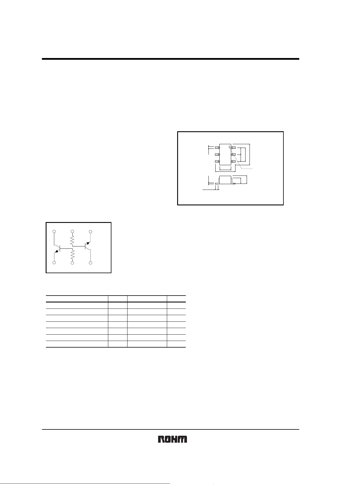
zStructure
NPN digital transistor
(Built-in resistor type)
zEquivalent circuit
(4) (5) (6)
zExternal dimensions (Unit : mm)
SMT6
)
)
6
(
1
(
0.3
)
5
(
)
4
(
1.6
2.8
0.15
0.3Min.
Abbreviated symbol : H21
0.95
1.9
)
2
(
0.95
)
3
(
1pin mark
0.8
Each lead has same dimensions
IMH21
2.9
1.1
R
1
1
R
(3) (2) (1)
R1=10kΩ
zAbsolute maximum ratings (Ta=25°C)
Parameter Symbol
Collector-base voltage
Collector-emitter voltage
Emitter-base voltage
Collector current
Collector power dissipation
Junction temperature
Storage temperature
∗ 200mW per element must not be exceeded.
V
CBO
V
CEO
V
EBO
I
C
C
Tj 150
Tstg
Limits
20
20
12
600
300(TOTAL)P
−55 to +150
Unit
V
V
V
mA
mW
°C
°C
∗
1/2
Transistor
zElectrical characteristics (Ta=25°C)
Parameter Symbol Min. Typ. Max. Unit Conditions
Collector-base breakdown voltage
Collector-emitter breakdown voltage
Emitter-base breakdown voltage
BV
BV
BV
Collector cutoff current
Emitter cutoff current
Collector-emitter saturation voltage
V
DC current transfer ratio
Input resistance
Transition frequency
Output "ON" resistance
∗
Transition frequency of the device.
zPackaging specifications and h
Package
Type
IMH21
Packaging type
Code
Basic ordering unit (pieces)
FE
SMT6
Taping
T110
3000
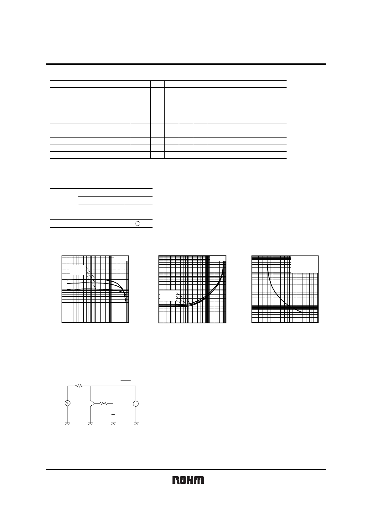
zElectrical characteristic curves
10000
Ta=100°C
Ta=25°C
FE
Ta= −40°C
1000
DC CURRENT GAIN : h
100
0.1 1 10 100 1000
COLLECTOR CURRENT : I
Fig.1 DC Current Gain vs.
Collector Current
VCE=5V
(mA)
C
zR
on measurement circuit
v
0
R
on
RL=1kΩ
= ×R
vi−v
0
20
CBO
CEO
EBO
I
CBO
I
EBO
CE (sat)
h
FE
R
1
f
T
R
on
−
20
−
12
−
−−
−−
40
−
820
−
710
150
−
0.9
−
− V
− V
− V
0.5 µA
0.5 µA
150 mV
2700 −
13 kΩ
− MHz
− Ω
10000
1000
(mV)
CE (sat)
100
Ta=100°C
Ta=25°C
Ta= −40°C
10
COLLECTOR SATURATION
VOLTAGE : V
1
0.1 1 10 100 1000
COLLECTOR CURRENT : I
Fig.2 Collector-Emitter Saturation
Voltage vs. Collector Current
L
=50µA
I
C
I
=1mA
C
I
=50µA
E
V
=20V
CB
=12V
V
EB
/ IB=50mA / 2.5mA
I
C
=5V, IC=50mA
V
CE
−
=10V, IE= −50mA, f=100MHz
V
CE
VI=5V, R
IC / IB=20
C
(mA)
=1kΩ, f=1KHz
L
1000
100
(Ω)
on
10
1
ON RESISTANCE : R
0.1
0.1 1 10 100
Fig.3
"ON" resistance vs. Input Voltage
∗
Ta=25°C
f=1kHz
R
hFE=250 (5V / 50mA)
INPUT VOLTAGE : V
IMH21
=1kΩ
L
(V)
I
Input
v
i
100mV
(rms)
f=1kHz
Fig.4 Output "ON" resistance (Ron)
measurement circuit
2/2
Output
V
v
0
v
I
 Loading...