

ROHM IMD6A Datasheet
EMD6 / UMD6N / IMD6A
Transistors
General purpose
(dual digital transistors)
EMD6 / UMD6N / IMD6A
!!!!
Features
1) Both the DTA143T chip and DTC143T chip in an EMT
or UMT or SMT package.
2) Mounting possible with EMT3 or UMT3 or SMT3
automatic mounting machines.
3) Transistor elements are independent, eliminating
interference.
4) Mounting cost and area can be cut in half.
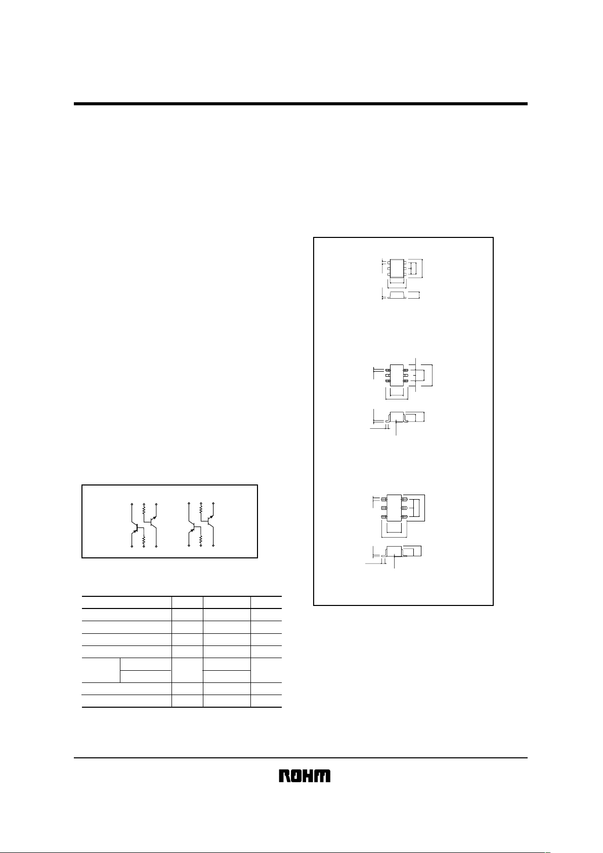
!!!!Structure
A PNP and NPN digital transistor
(each with a single built in resistor)
The following characteristics apply to both the DTr
1
and
DTr
2
, however, the “ −” sign on DTr2 values for the PNP
type have been omitted.
!!!!Equivalent circuit
EMD6 / UMD6N IMD6A
DTr
2
DTr
1
(3) (2) (1)
(3) (2) (1)
(4) (5) (6)
(4) (5) (6)
R
1
R
1
DTr
2
DTr
1
R
1
R
1
R1=4.7kΩR1=4.7kΩ
!!!!Absolute maximum ratings (Ta = 25°C)
Parameter Symbol
Limits
Unit
V
CBO
50 V
50
V
V
V
CEO
V
EBO
5
I
C
mA100
Tj 150 ˚C
Tstg −55∼+150 ˚C
P
C
EMD6, UMD6N 150 (TOTAL)
mW
IMD6A 300 (TOTAL)
∗
1
∗
2
Collector-base voltage
Collector-emitter voltage
Emitter-base voltage
Collector current
Junction temperature
Storage temperature
Collector
power
dissipation
∗
1 120mW per element must not be exceeded.
∗
2 200mW per element must not be exceeded.
!!!!
External dimensions
(Units : mm)
ROHM : EMT6
EMD6
ROHM : UMT6
EIAJ : SC-88
EMD6N
Abbreviated symbol : D6
Abbreviated symbol : D6
Abbreviated symbol : D6
ROHM : SMT6
EIAJ : SC-74
IMD6A
Each lead has same dimensions
Each lead has same dimensions
Each lead has same dimensions
0to0.1
(
6
)
2.0
1.3
0.9
0.15
0.7
0.1Min.
2.1
0.65
0.2
1.25
(
1
)
0.65
(
4
)
(
3
)
(
2
)
(
5
)
(
6
)
(
5
)
(
4
)
0.3to0.6
0.15
0.3
1.1
0.8
0to0.1
(
3
)
2.8
1.6
1.9
2.9
0.95
(
2
)
0.95
(
1
)
0.22
1.2
1.6
(1)
(2)(5)
(3)
(6)
(4)
0.13
0.5
0.5
0.5
1.0
1.6
EMD6 / UMD6N / IMD6A
Transistors
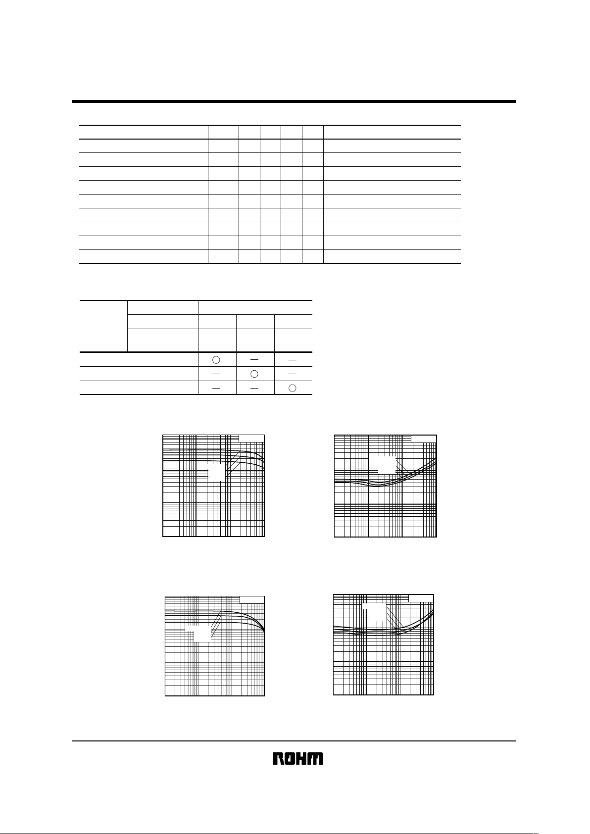
!!!!Electrical characteristics (Ta = 25°C)
Parameter Symbol
BV
CBO
BVCEO
BVEBO
ICBO
IEBO
hFE
VCE (sat)
R1
Min.
50
50
5
−
−
100
−
3.29
−
−
−
−
−
250
−
4.7
−
−
−
0.5
0.5
600
0.3
6.11
VI
C
=
50µA
I
C
=
1mA
I
E
=
50µA
V
CB
=
50V
V
EB
=
4V
V
CE
=
5V, IC=1mA
−
I
C/IB
=
5mA/0.25mA
V
V
µA
µA
−
V
kΩ
Typ. Max. Unit Conditions
fT
− 250 −
V
CE
=
10mA, IE=−5mA, f=100MHz
MHz
∗
Transition frequency of the transistor
∗
Collector-base breakdown voltage
Collector-emitter breakdown voltage
Emitter-base breakdown voltage
Collector cutoff current
Emitter cutoff current
DC current transfer ratio
Transition frequency
Collector-emitter saturation voltage
Input resistance
!!!!
Packaging specifications
Package
Code TR T148
3000 3000
Taping
Basic ordering
unit (pieces)
UMD6N
T2R
8000
EMD6
IMD6A
Type
!!!!Electrical characteristic curves
DTr
1
(NPN)
DC CURRENT GAIN : h
FE
COLLECTOR CURRENT : I
C
(A)
VCE=
5V
100µ 200µ 500µ 1m 2m 5m 10m 20m 50m100m
1k
500
200
100
50
20
10
5
2
1
Ta=100˚C
25˚C
−40˚C
Fig.1 DC current gain vs. collector
current
100µ200µ500µ1m 2m 5m 10m 20m 50m 100m
1
500m
200m
100m
50m
20m
10m
5m
2m
1m
COLLECTOR SATURATION VOLTAGE : V
CE (sat)
(
V)
COLLECTOR CURRENT : I
C
(A)
Ta=100˚C
25˚C
−40˚C
lC/lB=20
Fig.2 Collector-emitter saturation
voltage vs. collector current
DTr2 (PNP)
VCE=−5V
−100µ−1m
−10m
−200µ−2m
−20m
−500µ−5m
−50m−100m
1k
500
200
100
50
20
10
5
2
1
DC CURRENT GAIN : h
FE
COLLECTOR CURRENT : I
C
(A)
−40˚C
25˚C
Ta=100˚C
Fig.3 DC current gain vs. collector
current
lC/lB=20
−500m
−200m
−100m
−50m
−20m
−10m
−5m
−2m
−1m
−1
−100µ−1m
−10m
−200µ−2m
−20m
−500µ−5m
−50m−100m
COLLECTOR SATURATION VOLTAGE : VCE (sat)
(
V)
COLLECTOR CURRENT : IC
(A)
Ta=100˚C
25˚C
−40˚C
Fig.4 Collector-emitter saturation
voltage vs. collector current
 Loading...