

ROHM ES6U41 Technical data
2.5V Drive Nch+SBD MOSFET
ES6U41
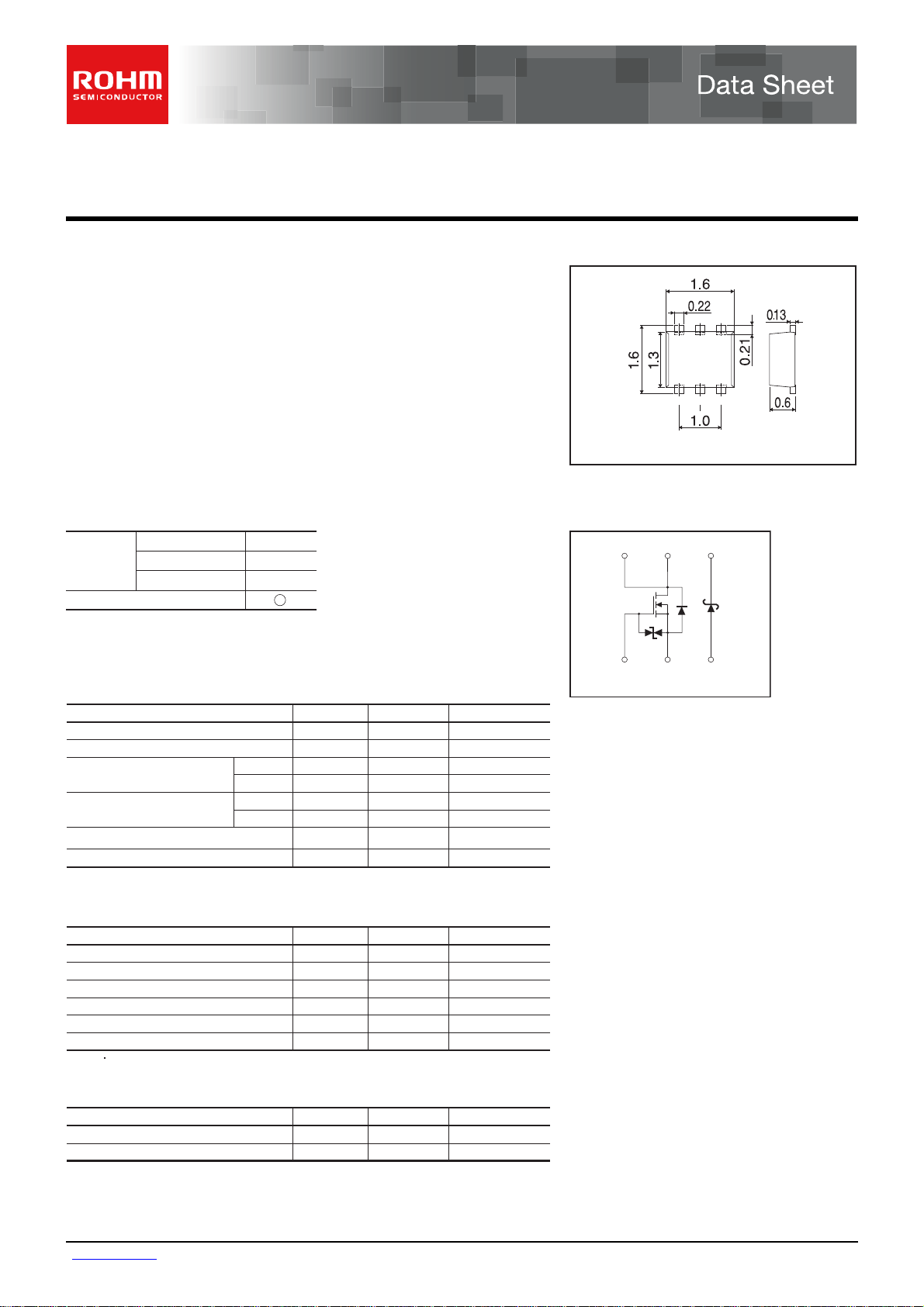
Structure Dimensions (Unit : mm)
Silicon N-channel MOSFET /
Schottky barrier diode
Features
1) Nch MOSFET and schottky barrier diodeare put in WEMT6 package.
2) High-speed switching, Low On-resistance.
3) Low voltage drive (2.5V drive).
4) Built-in Low V
F schottky barrier diode.
Applications
Switching
Package specifications Inner circuit
Type
ES6U41
Package
Code
Basic ordering unit (pieces)
Taping
T2R
8000
Absolute maximum ratings (Ta=25C)
<MOSFET>
Parameter
Drain-source voltage
Gate-source voltage
Drain current
Source current
(Body diode)
Continuous
Pulsed
Continuous
Pulsed
Channel temperature
Power dissipation W / ELEMENT0.7
∗1 Pw≤10μs, Duty cycle≤1%
∗2 Mounted on a ceramic board
Symbol
DSS
GSS
D
DP
S
SP
P
D
Limits Unit
30
±12
±1.5
∗1
±6.0
0.75
∗1
6.0
150
∗2
VV
VV
AI
AI
AI
AI
°CTch
<Di>
Parameter
Repetitive peak reverse voltage
Reverse voltage
Forward current
Forward current surge peak
Junction temperature
Power dissipation W / ELEMENT
∗1 60Hz 1cycle
∗2 Mounted on ceramic board
Symbol
RM
R
I
F
I
FSM
Tj
P
D
∗1
∗2
Limits Unit
25
20
0.5
2.0
150
VV
VV
A
A
°C
0.5
<MOSFET and Di>
Parameter Symbol
Power dissipation
Range of storage temperature
∗ Mounted on a ceramic board
∗
D
Limits Unit
0.8
−55 to +150
W / TOTALP
°CTstg
WEMT6
∗1 ESD protection diode
∗2 Body diode
(6) (5) (4)
(1) (2) (3)
Abbreviated symbol : U41
(6)
∗1
(1) (2)
(4)
(5)
∗2
(3)
(1)Gate
(2)Source
(3)Anode
(4)Cathode
(5)Drain
(6)Drain
www.rohm.com
1/4
○c 2012 ROHM Co., Ltd. All rights reserved.
2012.02 - Rev.B
ES6U41
Electrical characteristics
<MOSFET>
Parameter Symbol
Gate-source leakage
Drain-source breakdown voltage
Zero gate voltage drain current
Gate threshold voltage
Static drain-source on-state
resistance
Forward transfer admittance
Input capacitance
Output capacitance
Reverse transfer capacitance
Turn-on delay time
Rise time
Turn-off delay time
Fall time
Total gate charge
Gate-source charge
Gate-drain charge
∗Pulsed
<Body diode characteristics (Source-drain)>
Parameter Symbol
<Di>
Parameter Symbol
Forward voltage
Reverse current
I
V
(BR) DSS
I
V
GS (th)
R
DS (on)
C
C
C
t
d (on)
t
d (off)
Q
Q
V
GSS
DSS
Y
t
t
Q
V
I
oss
rss
SD
R
∗
∗
fs
iss
∗
∗
r
∗
∗
f
∗
g
∗
gs
∗
gd
F
Min.−Typ. Max.
Unit
−±10 μAVGS=±12V, VDS=0V
mΩ
mΩ
Unit
D
D
I
D
D
V
ID= 0.75A
V
R
R
V
ID= 1.5A, R
R
= 1mA, VGS=0V
DS
DS
= 1.5A, VGS= 4.5V
= 1.5A, VGS= 4V
= 1.5A, VGS= 2.5V
DS
DS
GS
DD
GS
L
G
DD
G
30 −−VI
−−1 μAV
0.5 − 1.5 V V
− 170 240 I
− 180 250 mΩ
− 240 340 I
1.5 −−SV
− 80 − pF V
− 1412− pF V
−
−
−
−
−
−
−
−−nC
− pF f=1MHz
7
− ns
9
− ns
15
− ns
6
− ns
1.6
2.2 nC
0.5
− nC
0.3
Min. Typ. Max.
−−1.2 V IS= 0.75A, VGS=0VForward voltage
Min. Typ. Max.
−−
−−
−−
Unit
0.36 V
0.52 V
100
μA
= 0.1A
I
F
= 0.5A
I
F
V
R
Conditions
= 30V, VGS=0V
= 10V, ID= 1mA
= 10V, ID= 1.5A
= 10V
=0V
15V
= 4.5V
20Ω
= 10Ω
15V, VGS= 4.5V
10Ω
L
= 10Ω
Conditions
Conditions
= 20V
Data Sheet
www.rohm.com
2/4
○c 2012 ROHM Co., Ltd. All rights reserved.
2012.02 - Rev.B
 Loading...