

Page 1
EMZ8 / UMZ8N
Transistors
Power management (dual transistors)
EMZ8 / UMZ8N
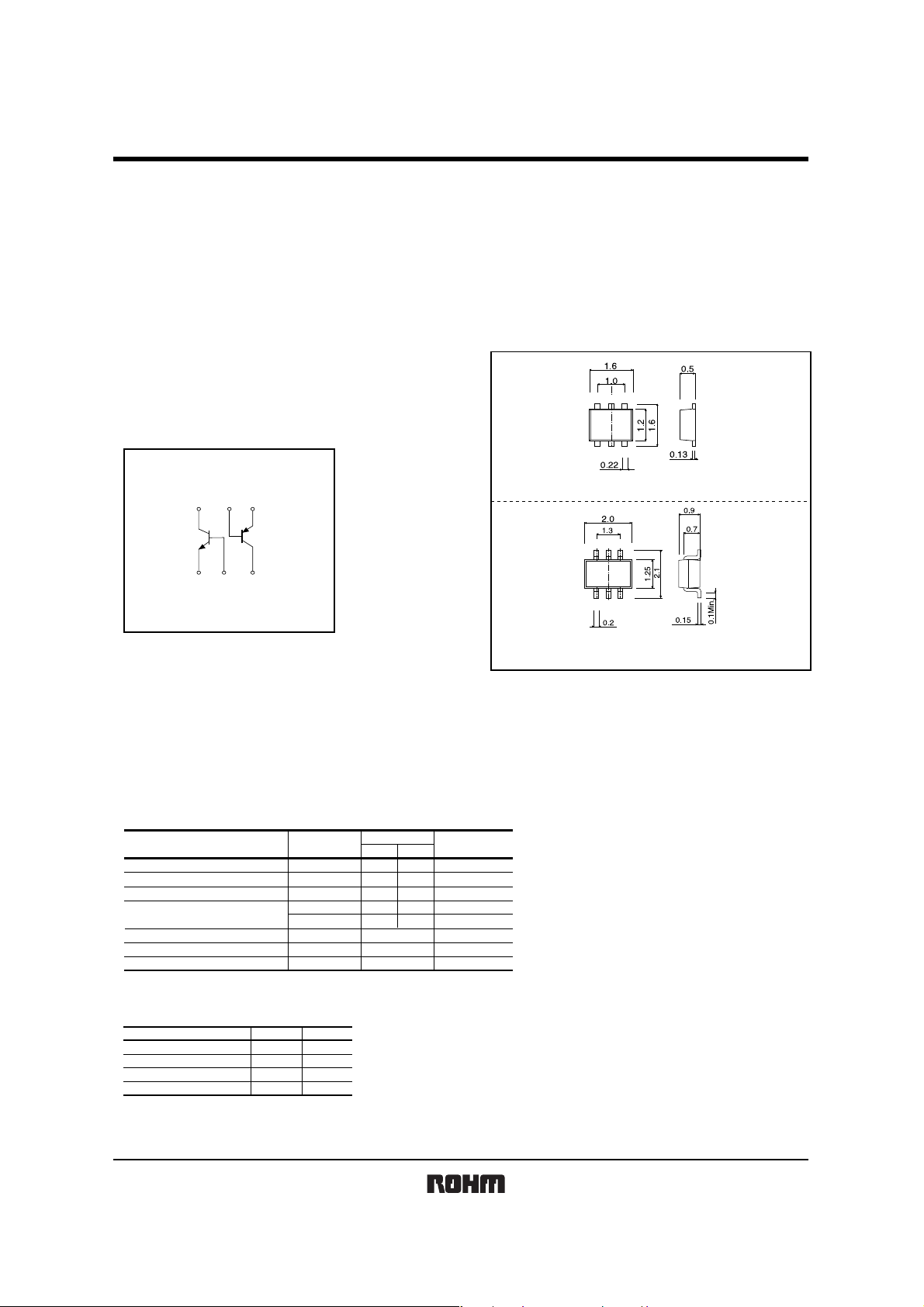
zFeature
1) Both a 2SA2018 chip and 2SC2412K chip in a EMT
or UMT package.
zEquivalent circuits
(3) (2) (1)
Tr
Tr
1
2
zDimensions(Unit : mm)
EMZ8
(6) (5) (4)
(1) (2) (3)
ROHM : EMT6
EIAJ :
UMZ8N
(6) (5)(4)
Each lead has same dimensions
(4) (5) (6)
zAbsolute maximum ratings (Ta=25°C)
Parameter Symbol
Collector-base voltage
Collector-emitter voltage
Emitter-base voltage
Collector current
Collector power dissipation
Junction temperature
Storage temperature
120mW per element must not be exceeded.
∗
V
V
V
I
Tstg
CBO
CEO
EBO
I
CP
Tj
C
C
Limits
Tr2
Tr1
60
−15
50
−12
7
−6
150
−500
−1 −
150 (TOTAL)
150
−55 to +150 °C
zPackage, marking, and packaging specifications
Part No. UMZ8N
Package
Marking
Code
Basic ordering unit (pieces)
EMZ8
EMT6
Z8
T2R
8000
UMT6
Z8
TR
3000
Unit
V
V
V
mA
A
mWP
°C
ROHM : UMT6
EIAJ : SC-88
∗
(1) (2)(3)
Each lead has same dimensions
Rev.C 1/4
Page 2
Transistors
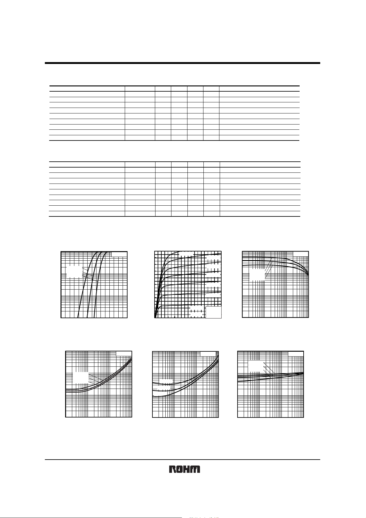
zElectrical characteristics (Ta=25°C)
Tr1
Collector-base breakdown voltage
Collector-emitter breakdown voltage
Emitter-base breakdown voltage
Collector cutoff current
Emitter cutoff current
Collector-emitter saturation voltage
DC current transfer ratio
Transition frequency
Output capacitance
Tr2
Collector-base breakdown voltage
Collector-emitter breakdown voltage
Emitter-base breakdown voltage
Collector cutoff current
Emitter cutoff current
Collector-emitter saturation voltage
DC current transfer ratio
Transition frequency
Output capacitance
z
Electrical characteristic curves
<Tr1>
1000
500
(mA)
200
C
100
50
20
10
5
2
COLLECTOR CURRENT : I
1
Fig.1 Grounded Emitter Propagation
1000
500
200
100
(V)
CE (sat)
COLLECTOR SATURATION
VOLTAGE : V
Parameter Symbol Min. Typ. Max. Unit Conditions
Parameter
VCE=2V
Ta=125°C
Ta=25°C
Ta= −40°C
0 0.5 1.0 1.5
BASE TO EMITTER VOLTAGE : V
(V)
BE
Characteristics
IC / IB=20
Ta=125°C
Ta=25°C
50
Ta= −40°C
20
10
5
2
1
1 2 5 10 20 50 100 200 500 1000
COLLECTOR CURRENT : I
C
(mA)
Fig.4 Collector-Emitter Saturation
Voltage vs.
Collector Current (Ι)
BV
BV
BV
V
CBO
CEO
EBO
I
CBO
I
EBO
CE(sat)
h
FE
f
T
Cob
−15 −−
−12
270
−
−0.1
260
6.5
−
−
−
−
−0.1
−
−0.1
−0.25
680
−
−
−
−6
−
−
−
−
−
µA
µA
MHz
pF
Symbol Min. Typ. Max. Unit
BV
BV
BV
V
CBO
CEO
EBO
I
CBO
I
EBO
CE(sat)
h
FE
T
f
Cob
60
−−
50
−
180
−
−
−
−
−
2
I
=700µA
B
−
−
0.1
0.1
0.4
560
−
3.5
(mA)
C
7
−
−
−
120
−
−
200
180
160
140
120
100
80
60
40
COLLECTOR CURRENT : I
20
0
0 0.2 0.4 0.6 0.8 1 1.2 1.4 1.6 1.8 2
IB=100µA
IB=0µA
µA
µA
MHz
pF
IB=600µA
I
=500µA
B
IB=400µA
IB=300µA
IB=200µA
Ta=25
pulsed
COLLECTOR TO EMITTER VOLTAGE : V
Fig.2 Typical Output Characteristics
1000
500
200
100
(mV)
50
IC / IB=50
CE (sat)
IC / IB=20
20
IC / IB=10
10
5
COLLECTOR SATURATION
VOLTAGE : V
2
1
1 2 5 10 20 50 100 200 500 1000
COLLECTOR CURRENT : I
Ta=25°C
(mA)
C
Fig.5 Collector-Emitter Saturation
Voltage vs.
Collector Current (ΙΙ)
V
IC = −10µA
V
=
−1mA
IC
V
IE
=
−10µA
=
−15V
VCB
=
−6V
VEB
V
−
V
V
V
V
−
=
−200mA/−10mA
IC/IB
VCE
=
−2V , IC = −10mA
=
−2V , IE = 10mA , f = 100MHz
VCE
=
−10V , IE = 0A , f = 1MHz
VCB
C
=
50µA
I
I
C
=
1mA
I
E
=
50µA
V
CB
=
60V
EB
=
7V
V
I
C/IB
=
50mA/5mA
CE
= 6V ,
I
C
=
V
CE
=
12V , I
E
V
V
°C
(V)
CE
=
CB
=
12V , I
E
= 0A , f =
1000
500
FE
200
100
50
20
10
5
DC CURRENT GAIN : h
2
1
1 2 5 10 20 50 100 200 500 1000
1mA
−2mA , f = 100MHz
Ta=125°C
Ta=25°C
Ta= −40°C
COLLECTOR CURRENT : I
Fig.3 DC Current Gain vs.
10000
(mV)
5000
BE (sat)
2000
1000
BASER SATURATION VOLTAGE : V
Ta= −40°C
Ta=25°C
Ta=125°C
500
200
100
50
20
10
1 2 5 10 20 50 100 200 500 1000
COLLECTOR CURRENT : I
Fig.6 Base-Emitter Saturation
Voltage vs.Collecter Current
EMZ8 / UMZ8N
Conditions
1MHz
Collector Current
VCE=2V
C
IC / IB=20
(mA)
C
(mA)
Rev.C 2/4
Page 3
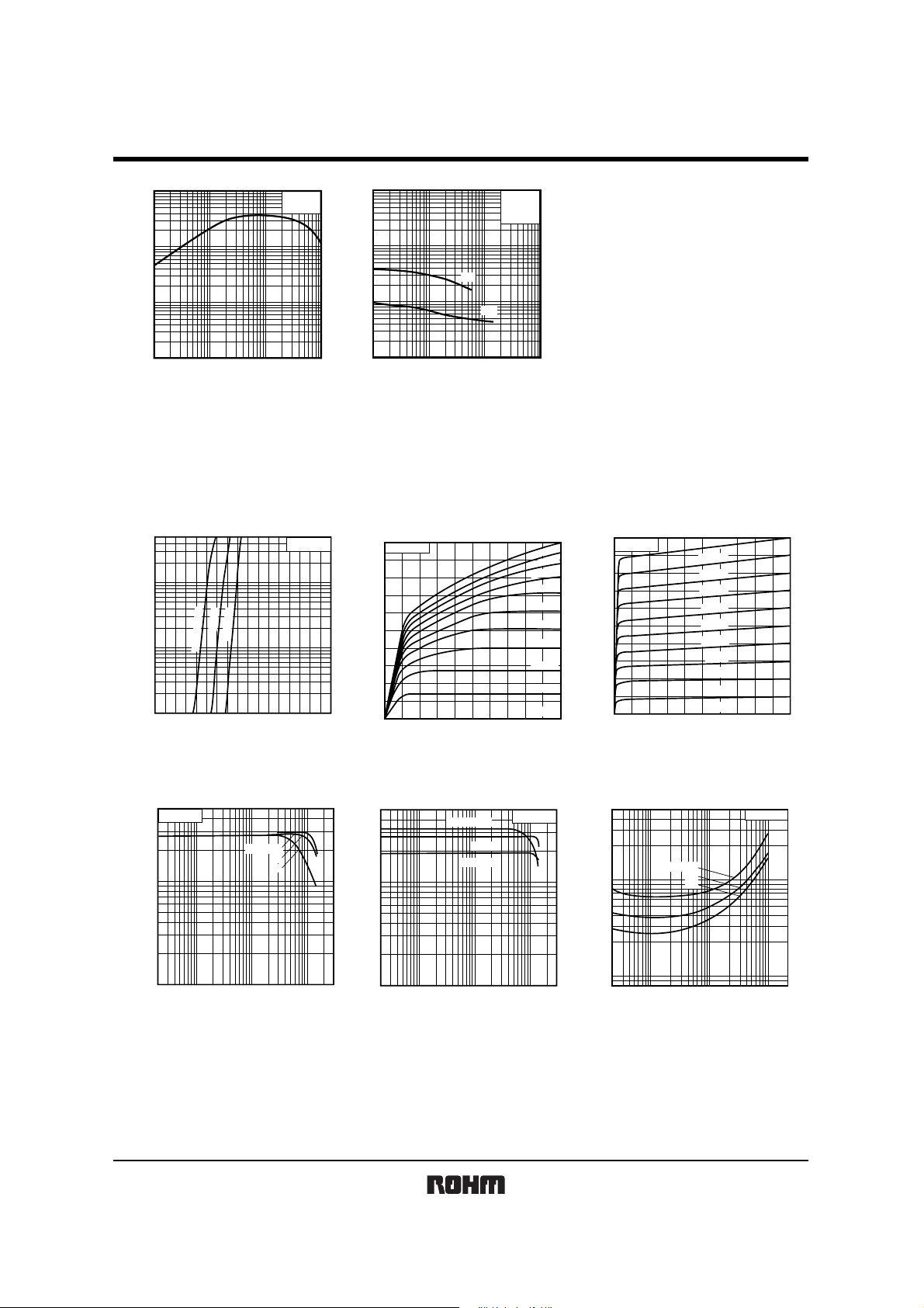
Transistors
1000
500
(MHz)
T
200
100
50
20
10
5
2
TRANSITION FREQUENCY : f
1
1 2 5 10 20 50 100 200 500 1000
EMITTER CURRENT : I
Fig.7 Gain Bandwidth Product vs.
Emitter Current
<Tr2>
50
20
(mA)
C
10
5
2
1
0.5
COLLECTOR CURRENT : I
0.2
0.1
0
0.2 0.4 0.6 0.8 1.0 1.2 1.4 1.6
BASE TO EMITTER VOLTAGE : V
Fig.1 Grounded emitter propagation
500
Ta=25°C
200
100
50
25°C
100°C
−55°C
=
Ta
characteristics
VCE=5V
C
3V
1V
VCE=2V
Ta=25°C
(mA)
V
CE
=6V
BE
1000
500
Cob (pF)
200
Cib (pF)
100
50
20
10
5
2
1
0.1 0.2 0.5 1 2 5 10 20 50 100
EMITTER INPUT CAPACITANCE :
COLLECTOR OUTPUT CAPACITANCE :
EMITTER TO BASE VOLTAGE : V
Cib
Fig.8 Collector Output Capacitance vs.
Collector-Base Voltage
Emitter Input Capacitance vs.
Emitter-Base Voltage
100
Ta=25°C
80
60
40
20
COLLECTOR CURRENT : IC (mA)
0
(V)
COLLECTOR TO EMITTER VOLTAGE : VCE (V)
0.4 0.8 1.2 1.6 2.00
Fig.2 Grounded emitter output
characteristics ( Ι )
500
FE
200
100
50
Ta=100°C
25°C
−55°C
Cob
IE=0A
f=1MHz
Ta=25°C
EB
VCE=
(V)
0.50mA
0.45mA
0.40mA
0.35mA
0.30mA
0.25mA
0.20mA
0.15mA
0.10mA
0.05mA
IB=0A
5V
10
(mA)
C
COLLECTOR CURRENT : I
COLLECTOR TO EMITTER VOLTAGE : V
0.5
(V)
CE(sat)
0.2
0.1
0.05
EMZ8 / UMZ8N
IC/IB=50
30µA
27µA
24µA
21µA
18µA
15µA
12µA
9µA
6µA
3µA
IB=0A
Ta=25°C
20
10
Ta=25°C
8
6
4
2
0
4 8 12 16
0
Fig.3 Grounded emitter output
characteristics ( ΙΙ )
20
CE
(V)
DC CURRENT GAIN : hFE
20
10
0.2
0.5 1 2 5 10 20 50 100 200
COLLECTOR CURRENT : IC (mA)
Fig.4 DC current gain vs.
collector current ( Ι )
DC CURRENT GAIN : h
20
10
0.2 0.5 1 2 5 10 20 50 100 200
COLLECTOR CURRENT : I
Fig.5 DC current gain vs.
collector current ( ΙΙ )
C
(mA)
0.02
0.01
COLLECTOR SATURATION VOLTAGE : V
0.2
0.5 1 2 5 10 20 50 100 200
COLLECTOR CURRENT : I
C
(mA)
Fig. 6 Collector-emitter saturation
voltage vs. collector current
Rev.C 3/4
Page 4
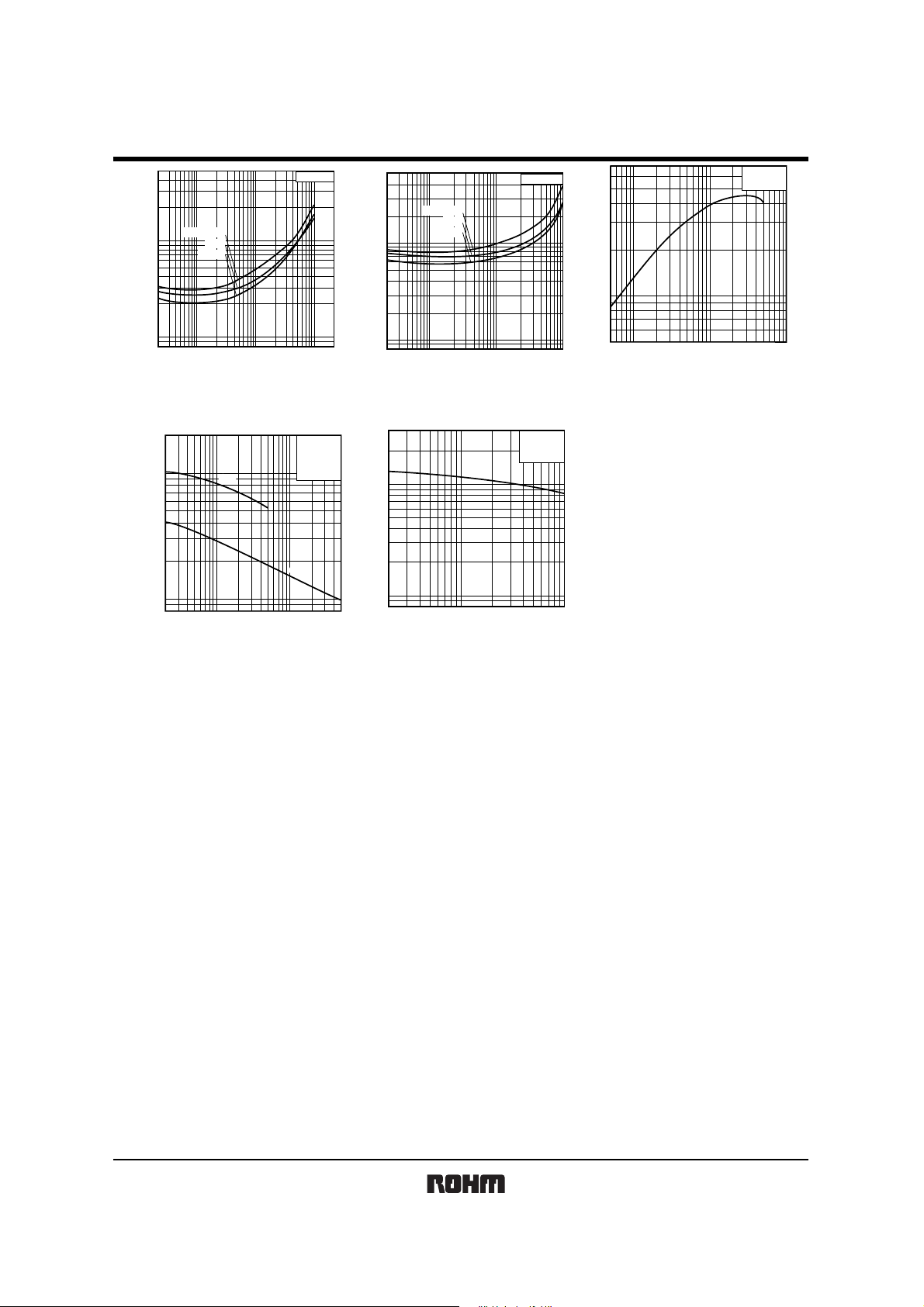
Transistors
0.5
(V)
CE(sat)
0.2
Ta=100°C
0.1
0.05
0.02
0.01
COLLECTOR SATURATION VOLTAGE : V
0.2
Fig.7 Collector-emitter saturation
20
pF)
pF)
10
25°C
−55°C
0.5 1 2 5 10 20 50 100 200
COLLECTOR CURRENT : I
C
voltage vs. collector current ( Ι )
Cib
IC/IB=10
(mA)
Ta=25°C
f=1MHz
IE
=0A
IC
=0A
0.5
(V)
CE(sat)
0.2
0.1
0.05
0.02
0.01
COLLECTOR SATURATION VOLTAGE : V
Ta=100°C
25°C
−55°C
0.2
0.5 1 2 5 10 20 50 100
COLLECTOR CURRENT : I
C
Fig.8 Collector-emitter saturation
voltage vs. collector current (ΙΙ)
bb' (ps)
200
100
IC/IB=50
(mA)
Ta=25°C
f=32MH
VCB=6V
EMZ8 / UMZ8N
500
(MHz)
T
200
100
TRANSITION FREQUENCY : f
50
−0.5 −1 −2 −5 −10 −20 −50 −100
EMITTER CURRENT : I
Fig.9 Gain bandwidth product vs.
emitter current
Z
Ta=25°C
E
(mA)
V
CE
=6V
5
2
EMITTER INPUT CAPACITANCE : Cib (
1
COLLECTOR OUTPUT CAPACITANCE : Cob (
0.2 0.5 1 2 5 10 20 50
COLLECTOR TO BASE VOLTAGE : VCB
EMITTER TO BASE VOLTAGE : VEB
Cob
(V)
(V)
Fig.10 Collector output capacitance vs.
collector-base voltage
Emitter input capacitance vs.
emitter-base voltage
50
20
10
−0.2 −0.5 −1 −2 −5 −10
BASE COLLECTOR TIME CONSTANT : Cc·r
EMITTER CURRENT : I
E
(mA)
Fig.11 Base-collector time constant
vs. emitter current
Rev.C 4/4
Page 5
Appendix
Notes
No technical content pages of this document may be reproduced in any form or transmitted by any
means without prior permission of ROHM CO.,LTD.
The contents described herein are subject to change without notice. The specifications for the
product described in this document are for reference only. Upon actual use, therefore, please request
that specifications to be separately delivered.
Application circuit diagrams and circuit constants contained herein are shown as examples of standard
use and operation. Please pay careful attention to the peripheral conditions when designing circuits
and deciding upon circuit constants in the set.
Any data, including, but not limited to application circuit diagrams information, described herein
are intended only as illustrations of such devices and not as the specifications for such devices. ROHM
CO.,LTD. disclaims any warranty that any use of such devices shall be free from infringement of any
third party's intellectual property rights or other proprietary rights, and further, assumes no liability of
whatsoever nature in the event of any such infringement, or arising from or connected with or related
to the use of such devices.
Upon the sale of any such devices, other than for buyer's right to use such devices itself, resell or
otherwise dispose of the same, no express or implied right or license to practice or commercially
exploit any intellectual property rights or other proprietary rights owned or controlled by
ROHM CO., LTD. is granted to any such buyer.
Products listed in this document are no antiradiation design.
The products listed in this document are designed to be used with ordinary electronic equipment or devices
(such as audio visual equipment, office-automation equipment, communications devices, electrical
appliances and electronic toys).
Should you intend to use these products with equipment or devices which require an extremely high level
of reliability and the malfunction of which would directly endanger human life (such as medical
instruments, transportation equipment, aerospace machinery, nuclear-reactor controllers, fuel controllers
and other safety devices), please be sure to consult with our sales representative in advance.
It is our top priority to supply products with the utmost quality and reliability. However, there is always a chance
of failure due to unexpected factors. Therefore, please take into account the derating characteristics and allow
for sufficient safety features, such as extra margin, anti-flammability, and fail-safe measures when designing in
order to prevent possible accidents that may result in bodily harm or fire caused by component failure. ROHM
cannot be held responsible for any damages arising from the use of the products under conditions out of the
range of the specifications or due to non-compliance with the NOTES specified in this catalog.
Thank you for your accessing to ROHM product informations.
More detail product informations and catalogs are available, please contact your nearest sales office.
ROHM Customer Support System
www.rohm.com
THE AMERICAS / EUROPE / ASIA / JAPAN
Contact us : webmaster@ rohm.co. jp
Copyright © 2008 ROHM CO.,LTD.
21 Saiin Mizosaki-cho, Ukyo-ku, Kyoto 615-8585, Japan
TEL : +81-75-311-2121
FAX : +81-75-315-0172
Appendix1-Rev2.0
 Loading...