

EMY1 / UMY1N / FMY1A
Transistors
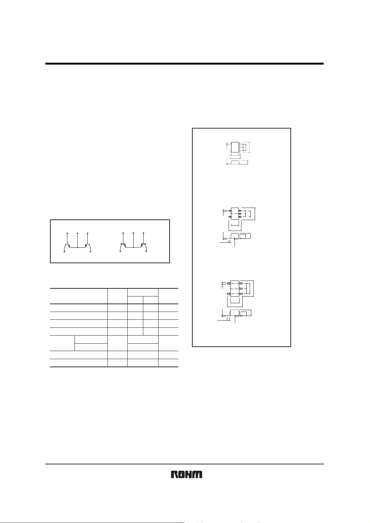
Emitter common (dual transistors)
EMY1 / UMY1N / FMY1A
zFeatures
1) Includes a 2SA1037AK and a 2SC2412K transistor in
a EMT or UMT or SMT package.
2) PNP and NPN transistors have common emitters.
3) Mounting cost and area can be cut in half.
zStructure
Epitaxial planar type
PNP / NPN silicon transistor
zEquivalent circuit
EMY1 / UMY1N FMY1A
(3) (2) (1)
Tr
2
(4)
Tr
1
(5)
(3) (4) (5)
Tr
2
(2)
Tr
1
(1)
zAbsolute maximum ratings (Ta = 25°C)
Parameter Symbol
Collector-base voltage
Collector-emitter voltage
Emitter-base voltage
V
V
V
Collector current
Power
dissipation
EMY1, UMY1N 150 (TOTAL)
FMY1A 300 (TOTAL)
Junction temperature
Storage temperature
1 120mW per element must not be exceeded.
∗
2 200mW per element must not be exceeded.
∗
Tstg −55 to +150
CBO
CEO
EBO
C
I
P
Tj 150
Limits
Tr
1
−60
−50
−6
−150
C
Tr
60
50
150
Unit
2
V
V
7
V
mA
∗1
mW
∗2
°C
°C
zExternal dimensions (Unit : mm)
EMY1
(3)
(4)
(2)
0.22
(1)
(5)
1.2
1.6
0.13
Each lead has same dimensions
ROHM : EMT5
Abbreviated symbol : Y1
UMY1N
ROHM : UMT5
EIAJ : SC-88A
Abbreviated symbol : Y1
0.2
0.1Min.
)
4
(
)
5
(
1.25
2.1
0.15
0~0.1
Each lead has same dimensions
)
3
(
)
1
(
FMY1A
)
)
3
2
(
(
0.3
0.15
0.3to0.6
ROHM : SMT5
EIAJ : SC-74A
Abbreviated symbol : Y1
)
4
(
)
)
1
5
(
(
1.6
2.8
0to0.1
Each lead has same dimensions
0.5
1.0
1.6
0.5
0.5
)
0.65
2
(
1.3
2.0
0.65
0.9
0.7
0.95
2.9
1.9
0.95
1.1
0.8
Rev.A 1/4
EMY1 / UMY1N / FMY1A
Transistors
zElectrical characteristics (Ta = 25°C)
1 (PNP)
Tr
Min.
Parameter Symbol
Collector-base breakdown voltage
Collector-emitter breakdown voltage
Emitter-base breakdown voltage
Collector cutoff current
Emitter cutoff current
Collector-emitter saturation voltage
DC current transfer ratio
Transition frequency
Output capacitance
BV
BV
BV
V
Cob
CBO
CEO
EBO
I
CBO
I
EBO
CE (sat)
h
FE
f
T
Tr
2 (NPN)
Parameter Symbol
Collector-base breakdown voltage
Collector-emitter breakdown voltage
Emitter-base breakdown voltage
Collector cutoff current
Emitter cutoff current
Collector-emitter saturation voltage
DC current transfer ratio
Transition frequency
Output capacitance
BV
BV
BV
V
I
CBO
I
EBO
CE (sat)
h
Cob
CBO
CEO
EBO
FE
f
T
zPackaging specifications
Packaging type
T2R
8000
Type
Code TR T148
Basic ordering
unit (pieces)
EMY1
UMY1N
FMY1
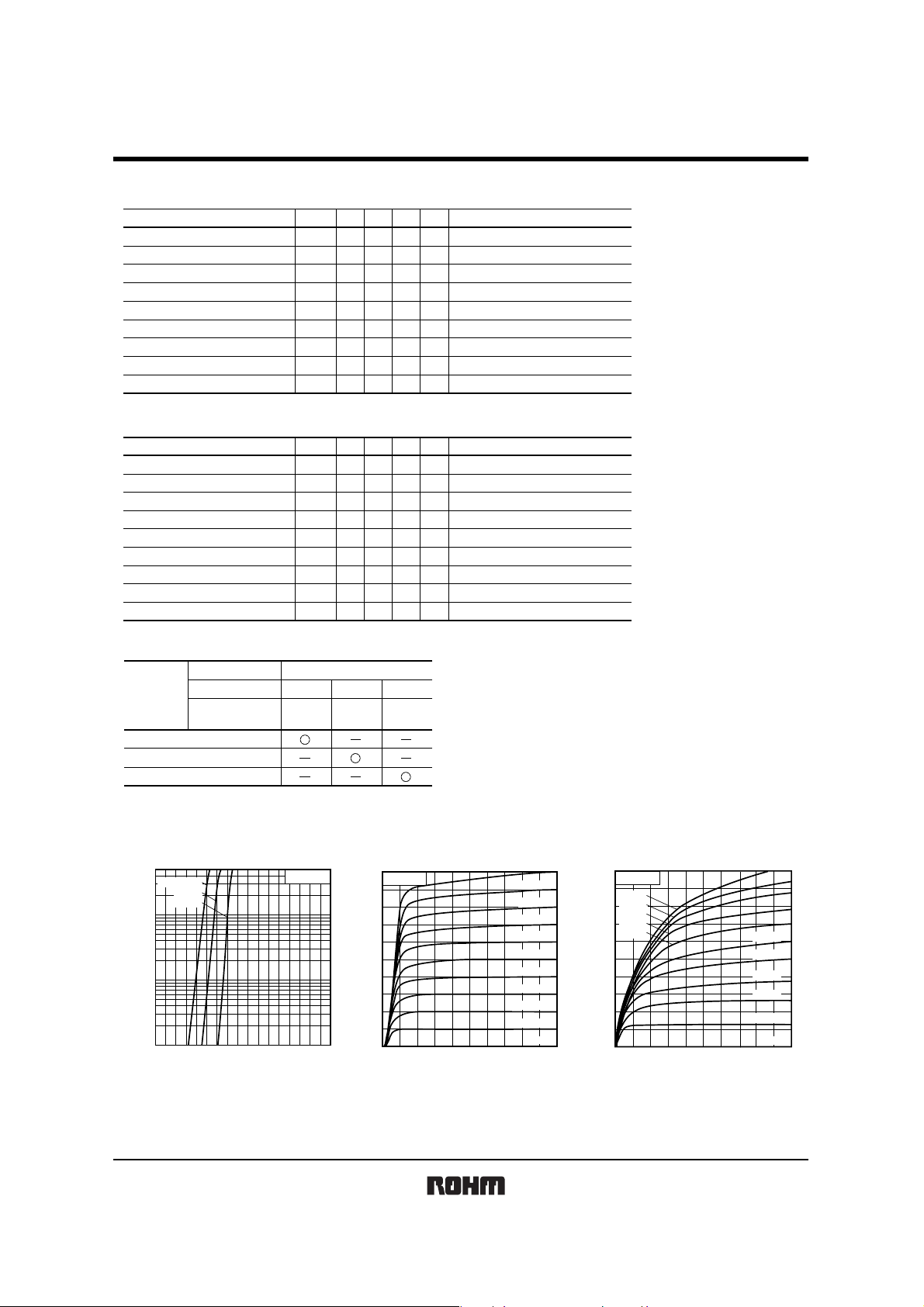
zElectrical characteristic curves
1 (PNP)
Tr
−50
Ta=100˚C
25˚C
−20
−40˚C
(mA)
−10
−5
−2
−1
−0.5
COLLECTOR CURRENT : Ic
−0.2
−0.1
−0.4 −0.6 −0.8 −1.0 −1.2 −1.4 −1.6
−0.2
BASE TO EMITTER VOLTAGE : VBE
VCE=−6V
(V)
Fig.1 Grounded emitter propagation
characteristics
Typ. Max. Unit Conditions
−
−60
−50
−6
−
−
−
120
− 140 −
−
Min.
60
50
7
−
−
−
120
− 180 −
−
−
VI
C
=
−50µA
−
−
−
−
−
−
4
−
−
−0.1
−0.1
−0.5
560
5
V
V
µA
µA
V
−
MHz
PF
C
=
−1mA
I
E
=
−50µA
I
CB
=
−60V
V
EB
=−6
V
I
C/IB
=
−50mA/−5mA
V
CE
=
−6V, I
V
CE
=
−12V, I
V
CB
=
−12V, I
V
Typ. Max. Unit Conditions
−
−
−
−
−
−
−
2
0.1
0.1
0.4
560
3.5
−
−
−
VI
V
V
µA
µA
V
−
MHz
PF
C
=
50µA
C
=
1mA
I
E
=
50µA
I
CB
V
EB
V
I
C/IB
V
CE
V
CE
V
CB
=
60V
=7
V
=
50mA/5mA
=
6V, I
=
12V, I
=
12V, I
Taping
3000 3000
−10
Ta=25˚C
−8
(mA)
−6
−4
−2
COLLECTOR CURRENT : IC
−0.4
COLLECTOR TO EMITTER VOLTAGE : VCE
−1.20
−0.8 −1.6 −2.0
Fig.2 Grounded emitter output
characteristics ( I )
C
=
−1mA
E
=
2mA, f=100MHz
E
=
0A, f=1MHz
C
=
1mA
E
=−
2mA, f=100MHz
E
=
0A, f=1MHz
−35.0
−31.5
−28.0
−24.5
−21.0
−17.5
−14.0
−10.5
−7.0
−3.5µA
B=0
I
−100
−80
(mA)
C
−60
−40
−20
COLLECTOR CURRENT : I
(V)
Ta=25˚C
−500
−450
−400
−350
−300
0
COLLECTOR TO EMITTER VOLTAGE : V
−250
−200
−150
−100
−50µA
Fig.3 Grounded emitter output
characteristics ( II )
Rev.A 2/4
IB=0
−5−3 −4−2−1
CE
(V)
 Loading...