

EMF9
Transistors
Power management (dual transistors)
EMF9
2SC5585 and 2SK3019 are housed independently in a EMT6 package.
zApplication
Power management circ uit
zFeatures
1) Power switching circuit in a single package.
2) Mounting cost and area can be cut in half.
zStructure
Silicon epitaxial planar transistor
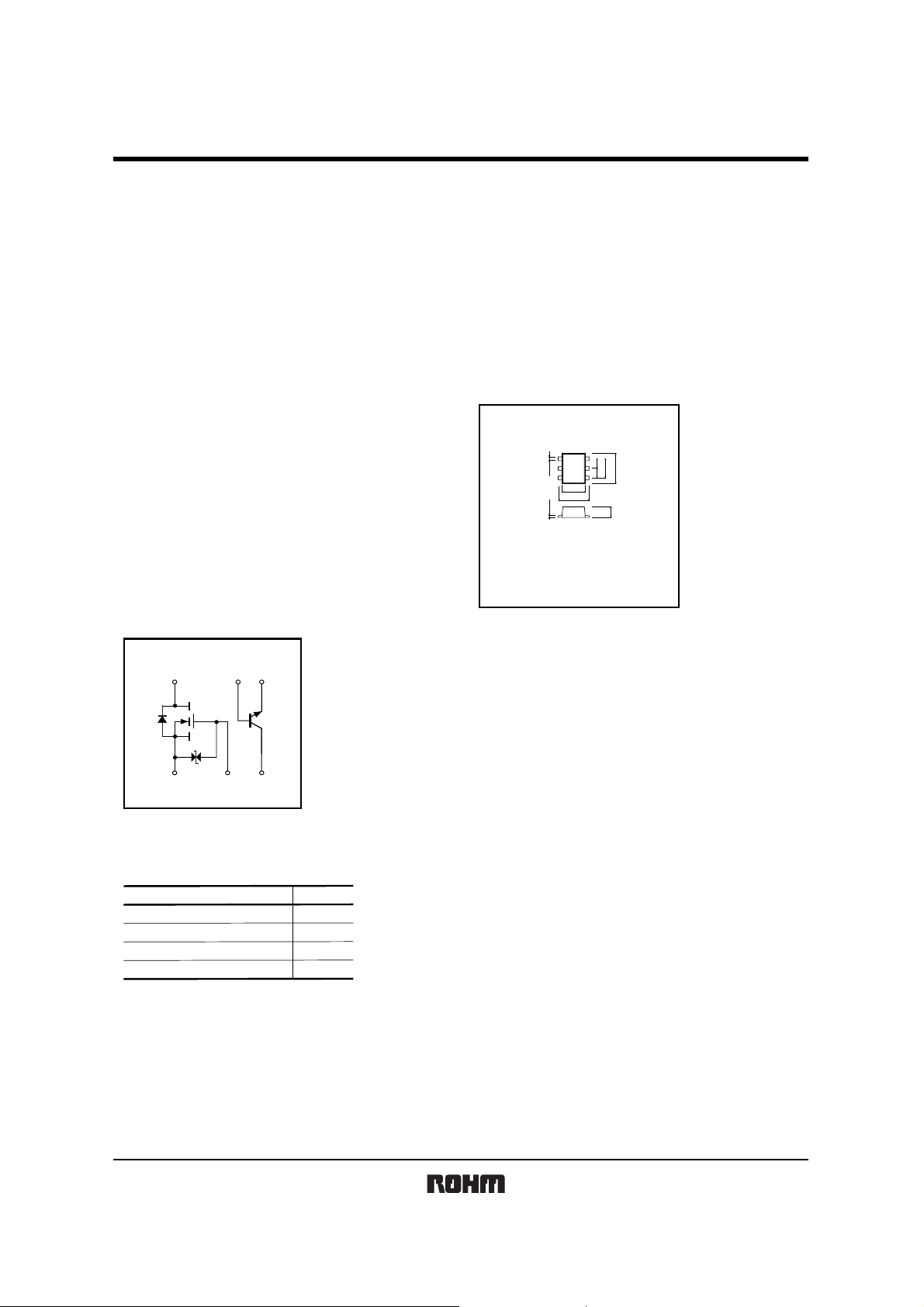
zEquivalent circuit s
(1)(2)(3)
Tr2
(4) (5) (6)
Tr1
zPackaging specifications
Type
Package
Marking
Code
Basic ordering unit (pieces)
EMF9
EMT6
F9
T2R
8000
zDimensions (Units : mm)
(3)
ROHM : EMT6
Abbreviated symbol : F9
0.22
0.13
(4)
(6)
0.5
1.0
1.6
(2)(5)
0.5
(1)
1.2
1.6
0.5
Each lead has
same dimensions
Rev.A 1/5
EMF9
Transistors
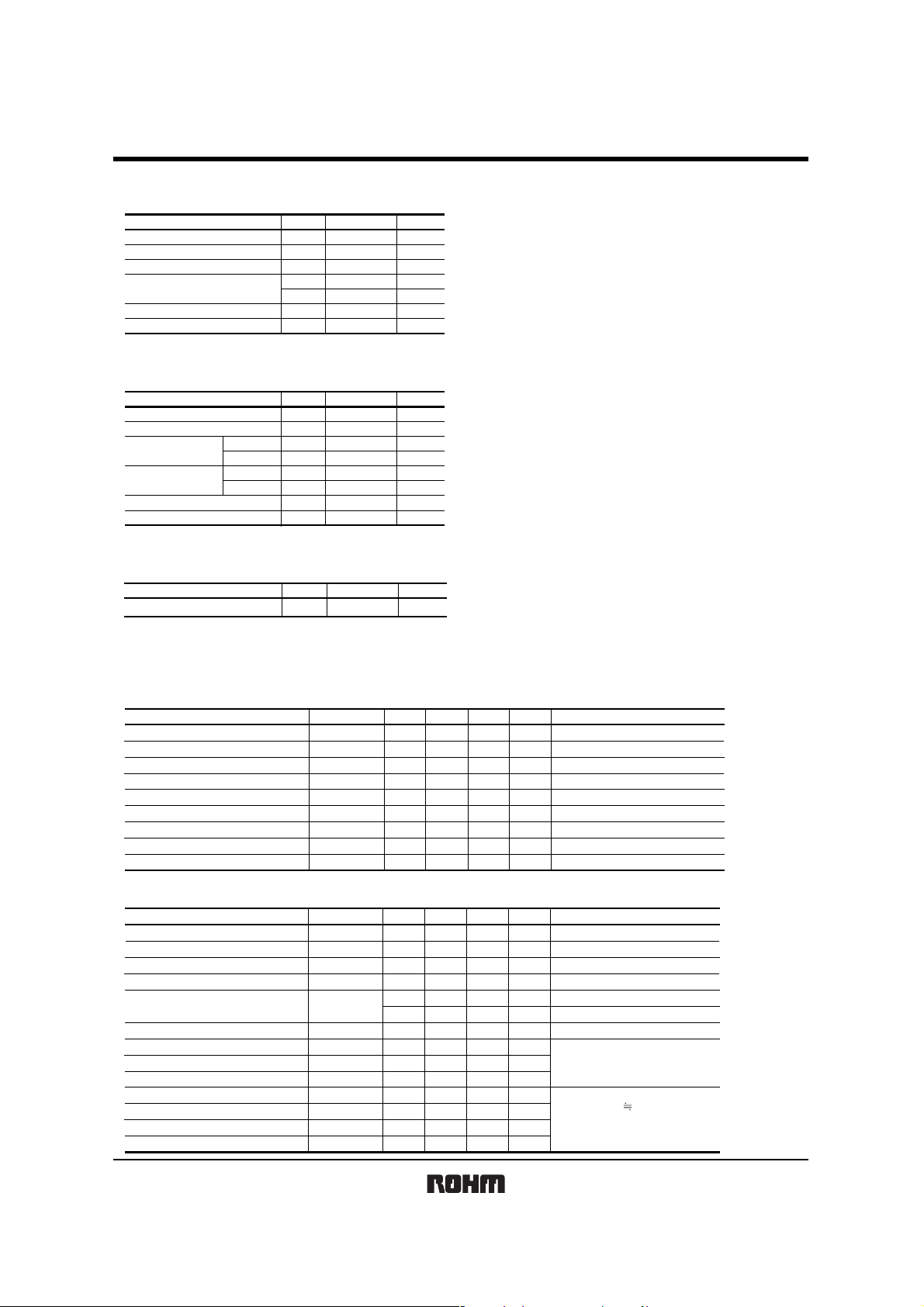
zAbsolute maximum ratings (Ta=25°C)
Tr1
Collector-base voltage
Parameter Symbol
Collector-emitter voltage
Emitter-base voltage
Collector current
Junction temperature
Range of storage temperature
∗ Single pulse PW=1ms
CBO
V
V
CEO
V
EBO
I
I
CP
Tj
Tstg
C
Limits
15
12
6
500
1.0
150
−55~+150
Tr2
Drain-source voltage
Parameter
Gate-source voltage
Drain current
Reverse drain
current
Continuous
Pulsed
Continuous
Pulsed
Channel temperature
Range of storage temperature
∗ PW≤10ms Duty cycle≤50%
Symbol
DSS
V
V
GSS
I
DP
I
I
DR
I
DRP
Tch
Tstg
D
Limits
30
±20
100
200 mA
100 mA
200
150
−55~+150
Tr1, Tr2
D
Limits
150(TOTAL)
Parameter
Total power dissipation
∗ 120mW per element must not be exceeded. Each terminal mounted on a recommended land.
Symbol
P
zElectrical characteristics (T a=25°C)
Tr1
Parameter Symbol Min. Typ. Max. Unit Conditions
CEO
Collector-emitter breakdown voltage
Collector-base breakdown voltage
Emitter-base breakdown voltage
Collector cut-off current
Emitter cut-off current
Collector-emitter saturation voltage
DC current gain
Transition frequency
Collector output capacitance
BV
CBO
BV
EBO
BV
CBO
I
EBO
I
CE(sat)
V
FE
h
f
T
Cob − 7.5 −
Tr2
Parameter
Gate-source leakage
Drain-source breakdown voltage
Zero gate voltage drain current
Gate-threshold voltage
Static drain-source
on-state resistance
Forward transfer admittance
Input capacitance
Output capacitance
Reverce transfer capacitance
Turn-on delay time
Rise time
Turn-off delay time
Fall time
Symbol
I
GSS
(BR)DSS
V
DSS
I
V
GS(th)
DS(on)
R
|Y
fs
C
iss
C
oss
C
rss
t
d(on)
r
t
t
d(off)
f
t
|
Unit
V
V
V
mA
∗
A
°C
°C
Unit
V
V
mA
∗
∗
mA
°C
°C
Unit
∗
mW
12
−−
15
−−
6
−−
−−
−−
− 100
100
100
250 mV
270 − 680
320
−
Min. Typ. Max. Unit Conditions
−−
30
−−
−−
0.8
−
−
20
−
−
−
−
−
−
−
1.0 µA
1.5
−
58Ω
713Ω
−−mS V
13
9
4
15
35
80
80
MHz
−
±1 µA
−
− pF
− pF
− ns
−
− ns
− ns
V
I
C
=1mA
V
I
C
=10µA
V
I
E
=10µA
nA VCB=15V
nA VEB=6V
IC=200mA, IB=10mA
− V
CE
=2V, IC=10mA
VCE=2V, IE=−10mA, f=100MHz
CB
=10V, IE=0mA, f=1MHz
V
pF
VGS=±20V, VDS=0V
V
I
D
=10µA, VGS=0V
VDS=30V, VGS=0V
VV
DS
=3V, ID=100µA
ID=10mA, VGS=4V
D
=1mA, VGS=2.5V
I
DS
=3V, ID=10mA
pF
DS
=5V, VGS=0V, f=1MHz
V
D
=10mA, VDD 5V,
I
ns
GS
=5V, RL=500Ω,
V
R
GS
=10Ω
Rev.A 2/5
 Loading...