

EMF33
Transistors
Power management,
Dual-chip Bipolar Transistor
EMF33
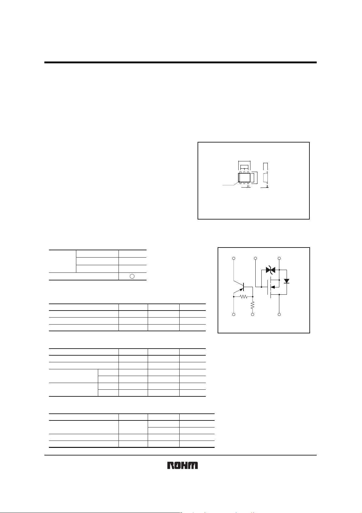
zApplications zDimensions (Unit : mm)
Power management circ uit
zFeatures
1) DTB513Z (digital transistor) and 2SK3019 (MOS FET) are
housed independently in the EMT6 packa ge.
2) Power switching circuit in a single package.
3) Mounting cost and area can be cut in half.
zStructure
Epitaxial Plannar Silicon T ransistor
zPackaging specifications
zEquivalent circuit
EMT6
0.5
(6)
(2)
(1)
1pin mark
0.22
Abbreviated symbol : F33
1.6
1.0
0.5
(5)
(3)
0.5
(4)
1.2
1.6
0.13
Each lead has same dimensions
Type
Package
Code
Basic ordering unit (pieces)
Taping
T2R
8000
EMF33
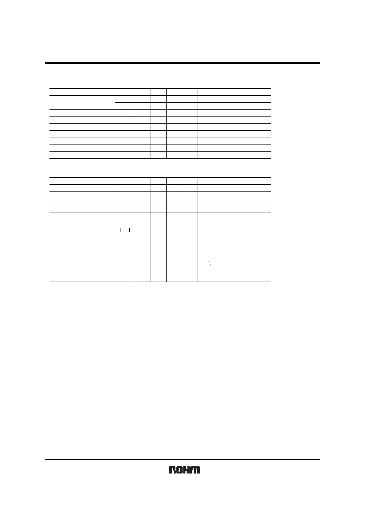
zAbsolute maximum ratings (Ta=25°C)
<Tr1>
Parameter
Supply voltage
Input voltage
Collector current
∗ Characteristics of built-in transistor.
Symbol
CC
IN
I
C(max)
<Tr2>
Parameter
Drain-source voltage
Gate-source voltage
Drain current
Reverse drain current
∗ PW≤10ms DUTY CYCLE≤50%
Continous
Pulsed
Continous
Pulsed
Symbol
DSS
GSS
I
D
I
DP
I
DR
I
DRP
<Tr1, Tr2 in common>
Parameter
Power dissipation
Junction temperature
Range of storage temperature
∗ Each terminal mounted on a recommended land.
Symbol
P
D
Tj
Tstg
Limits Unit
−12
−10 to +5
∗
−500
Limits Unit
30
±20
100
∗
∗
Limits Unit
150
∗
120
150
VV
VV
mA
VV
VV
mA
mA200
mA100
mA200
mW / TOTAL
mW / ELEMENT
°C
°C−55 to +150
Tr1
∗1 ESD protection diode
∗2 Body diode
1/R2
=1kΩ/10kΩ
Tr1 : R
Tr2 : MOS FET
(4)(5)(6)
∗1
Tr2
∗2
R
2
R
1
(3)(2)(1)
(1) Emitter
(2) Base
(3) Drain
(4) Source
(5) Gate
(6) Collector
Rev.A 1/4
Transistors
zElectrical characteristics (T a=25°C)
<Tr1>
Parameter Symbol
V
Input voltage
Output voltage
Input current
Output current
DC current gain
Transition frequency
Input resistance
Resistance ratio
∗ Characteristics of built-in transistor.
<Tr2>
Parameter Symbol
Gate-source leakage
Drain-source breakdown voltage
Zero gate voltage drain current
Gate-threshold voltage
Static drain-source on-resistance
Forward transfer admittance
Input capacitance
Output capacitance
Reverse transfer capacitance
Turn-on delay time
Rise time
Turn-off delay time
Fall time
I(off)
V
I(on)
V
O(on)
I
I
I
O(off)
I
∗
f
T
R1
R2/R1 8 10 12 −
I
GSS
V
(BR)DSS
I
DSS
V
GS(th)
R
DS(on)
Y
fs
C
iss
C
oss
C
rss
d(on)
t
r
t
d(off)
t
f
t
Min.
Typ. Max.
Unit
−−−0.3 V V
CC
Conditions
= −5V, IO= −100µA
−2.5 −−VVO= −0.3V, IO= −20mA
−−60 −300 mV VO= −100mA, II= −5mA
−−−6.4 mA VI= −5V
−−−0.5 uA VCC= −12V, VI= 0V
140
−−
− 260 −−V
−
= −5V, IO= −100mAG
V
O
= −10V, IE= 5mA, f=100MHz
CE
0.7 1 1.3 kΩ
Min.
Typ. Max.
−−±1 µAV
Unit
GS
Conditions
= ±20V, VDS=0V
30 −−−ID= 10µA, VGS=0A
−−1.0 µAVDS= 30V, VGS=0V
0.8 − 1.5 V VDS= 3V, ID=100µA
−
58
−
713
20 −−ms V
− 13 − pF
− 9 − pF
− 4 − pF
− 15 − ns
− 35 − ns
− 80 − ns
− 80 − ns
Ω
= 10mA, VGS= 4V
I
D
Ω
= 1mA, VGS= 2.5V
I
D
DS
V
DS
GS
V
f=1MHz
I
= 10mA
D
V
DD
V
GS
R
= 500Ω
L
R
GS
= 3V, ID= 10mA
= 5V
= 0V
= 5V
= 5V
= 10Ω
EMF33
Rev.A 2/4
 Loading...