

Datasheet
www.rohm.com
© 2012 ROHM Co., Ltd. All rights reserved.
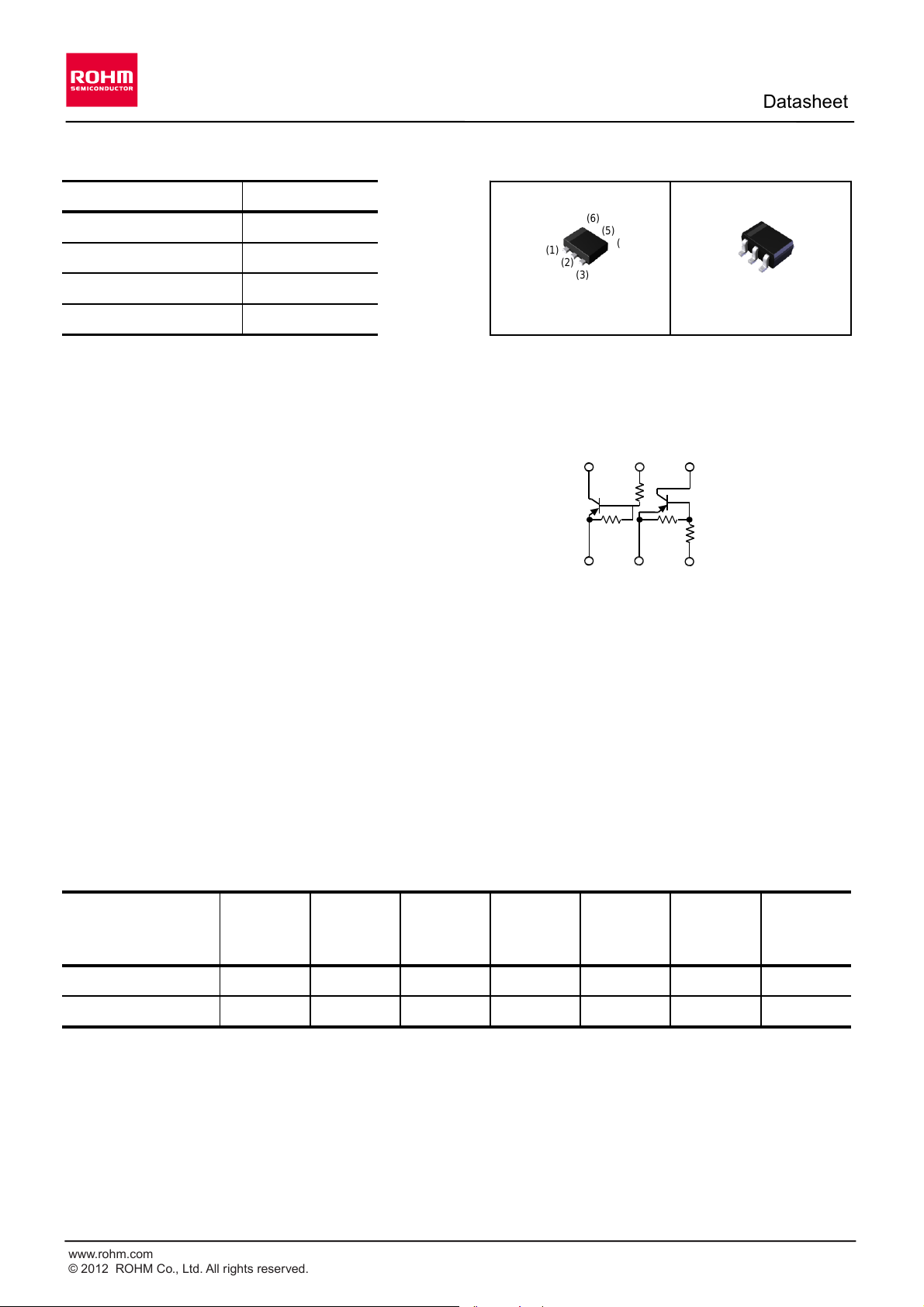
EMB6 / UMB6N
PNP -100mA -50V Complex Digital Transistors (Bias Resistor Built-in Transistors)
l
Outline
l
Features
l
Inner circuit
1) Built-In Biasing Resistors, R1 = R2 = 47kW.
2) Two DTA144E chips in one package.
3) Built-in bias resistors enable the configuration of
an inverter circuit without connecting external
input resistors (see inner circuit).
4) The bias resistors consist of thin-film resistors
with complete isolation to allow negative biasing
of the input. They also have the advantage of
completely eliminating parasitic effects.
5) Only the on/off conditions need to be set for
operation, making the circuit design easy.
6) Lead Free/RoHS Compliant.
l
Application
Inverter circuit, Interface circuit, Driver circuit
l
Packaging specifications
UMB6N
UMT6
2021
TR
180
8
8,000B68
Tape width
(mm)
Basic
ordering
unit (pcs)
Marking
Reel size
(mm)
EMB6
EMT6
1616
T2R
180
3,000
B6
Part No.
Package
Package
size
(mm)
Taping
code
R
1
47kW
Parameter
Tr1 and Tr2
V
CC
-50V
I
C(MAX.)
-100mA
EMT6
UMT6
R
2
47kW
EMB6
(SC-107C)
UMB6N
SOT-353 (SC-88)
OUT
(6)
(2)
GND
(1)
GND
(3)
IN
IN
(5)
OUT
(4)
(6)
(5)
(4)
(1)
(2)
(3)
(6)
(5)
(4)
(1)
(2)
(3)
1/6
2012.06 - Rev.B

www.rohm.com
© 2012 ROHM Co., Ltd. All rights reserved.
Data Sheet
EMB6 / UMB6N
lAbsolute maximum ratings (Ta = 25°C)
<For Tr1 and Tr2 in common>
Supply voltage
Input voltage
Output current
Collector current
Power dissipation
Junction temperature
Range of storage temperature
lElectrical characteristics(Ta = 25°C)
<For Tr1 and Tr2 in common>
*1 Characteristics of built-in transistor
*2 Each terminal mounted on a reference footprint
*3 120mW per element must not be exceeded.
Output voltage
V
O(on)
IO / II = -10mA / -0.5mA
MHz
-
250
-
mAmA-
-
-0.18
68--
-
-
-
-0.5
kW
0.811.2-32.9
47
61.1V-
-
-3.0
-V-
-0.1
-0.3
-
-0.5
Parameter
Symbol
Input voltage
V
I(off)
V
CC
= -5V, IO = -100mA
V
I(on)
VO = -0.3V, IO = -2mA
Unit
Min.
Typ.
Max.
T
j
150
°C
T
stg
-55 to +150
°C
Conditions
I
C(MAX.)
*1
-100
mA
150 (Total)
*3
mW
P
D
*2
V
IN
-40 to +10
V
I
O
-30
mA
Parameter
Symbol
Values
Unit
V
CC
-50
V
Input current
I
I
VI = -5V
Output current
I
O(off)
V
CC
= -50V, VI = 0V
DC current gain
G
I
VO = -5V, IO = -5mA
Input resistance
R
1
-
Resistance ratio
R2/R
1
-
Transition frequency
fT
*1
V
CE
= -10V, IE = 5mA,
f = 100MHz
2/6
2012.06 - Rev.B
www.rohm.com
© 2012 ROHM Co., Ltd. All rights reserved.
Data Sheet
EMB6 / UMB6N
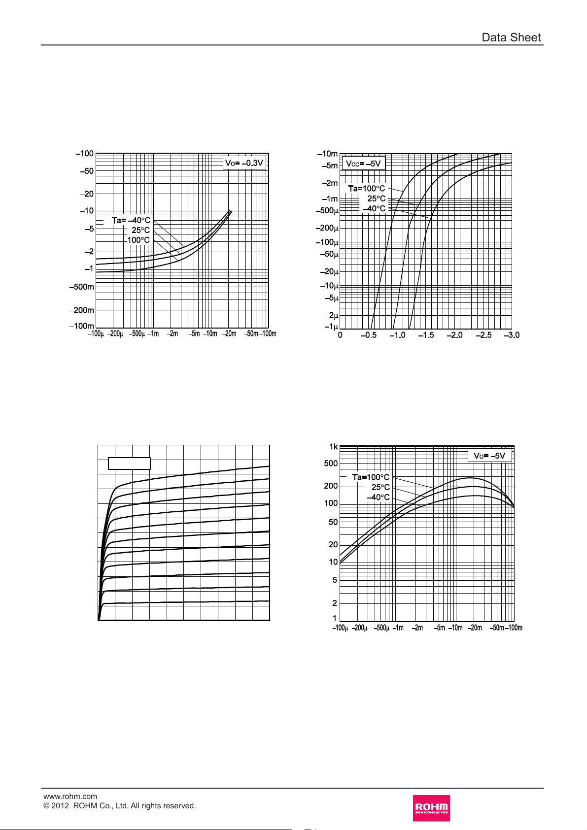
lElectrical characteristic curves(Ta = 25°C)
Fig.1 Input voltage vs. output current
(ON characteristics)
INPUT VOLTAGE : V
I(on)
[V]
OUTPUT CURRENT : IO [A]
Fig.2 Output current vs. input voltage
(OFF characteristics)
OUTPUT CURRENT : I
O
[A]
INPUT VOLTAGE : V
I(off)
[V]
Fig.3 Output current vs. output voltage
OUTPUT CURRENT : I
O
[mA]
OUTPUT VOLTAGE : VO [V]
Fig.4 DC current gain vs. output current
DC CURRENT GAIN : G
I
OUTPUT CURRENT : IO [A]
0
-5
-10
-15
-20
-25
-30
0 -5 -10
-40μA
0A
-60μA
-70μA
-80μA
-90μA
-100μA
-110μA
-120μA
-130μA
II=
Ta=25ºC
-30μA
-50μA
3/6
2012.06 - Rev.B
 Loading...