ROHM DTD543EE, DTD543EM Technical data

R
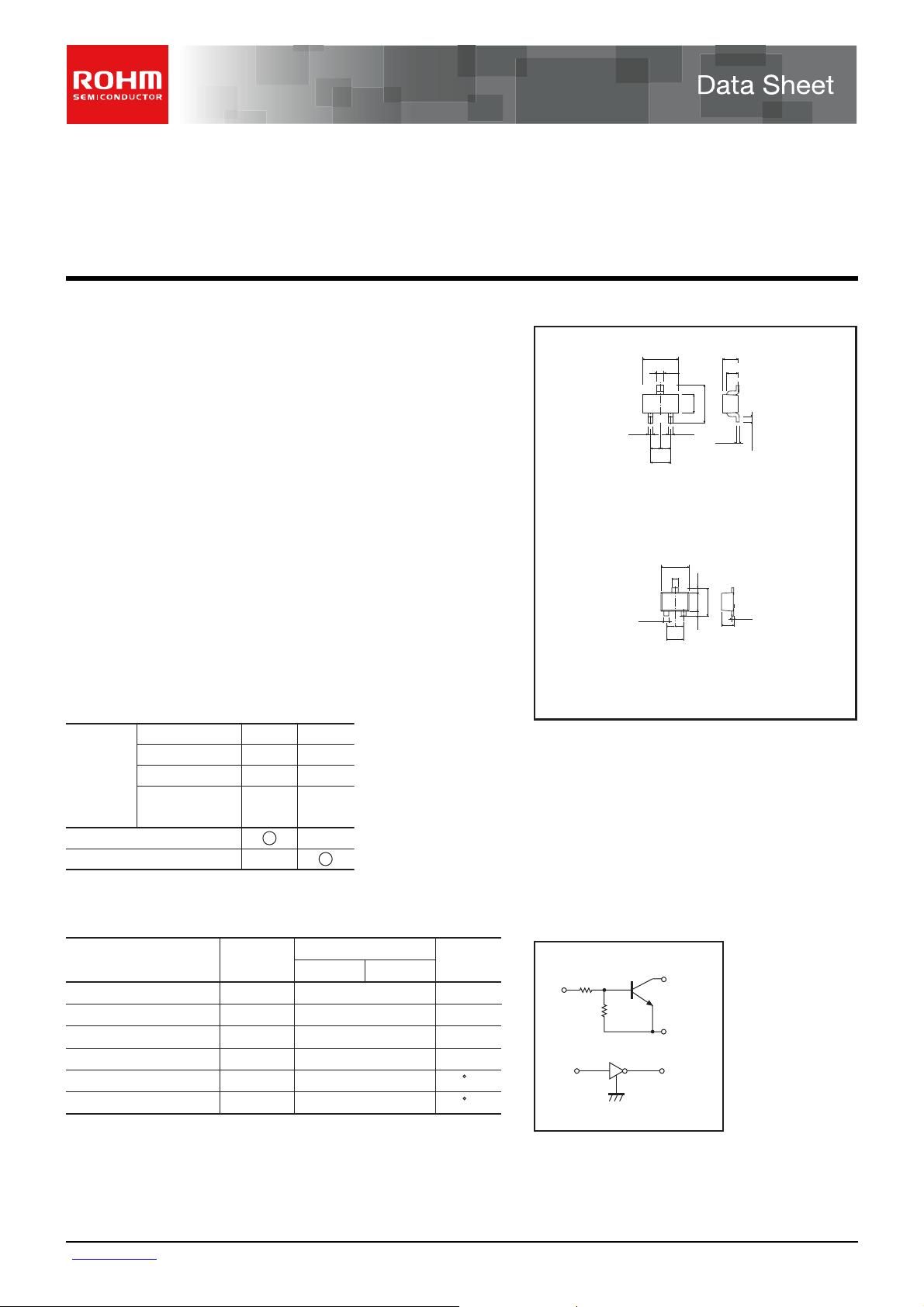
Low VCE (sat) Digital transistors
(with built-in resistors)
DTD543EE / DTD543EM
zApplications zDimensions (Unit : mm)
Inverter, Interface, Driver
zStructure
NPN digital transistor (Built-in resistor type)
zFeature
1. V
CE (sat) is lower than conventional products.
2. Built-in bias resistors enable the configuration of
an inverter circuit without connecting
external input resistors (see equivalent circuit).
3. The bias resistors consist of thin-film resistors with
complete isolation to allow negative biasing of the input.
They also have the advantage of almost completely
eliminating parasitic effects.
4. Only the on / off conditions need to be set for operation,
making device design easy.
zPackaging specifications
EMT3 VMT3
TL
3000
T2L
8000
−
−
Part No.
DTD543EE
DTD543EM
Package
Packaging type Taping Taping
Code
Basic ordering
unit (pieces)
zAbsolute maximum ratings (Ta=25°C) zInner circuit
Parameter
Supply voltage
Input voltage
Collector current
Power dissipation
Junction temperature
Storage temperature
∗1 Characteristics of built-in transistor.
∗2 Each terminal mounted on a recommended land.
Symbol
V
CC
IN
V
∗1
∗2
C (max)
I
PD
Tj
Tstg
DTD543EE DTD543EM
Limits
12
−10 to +12
500
150
150
−55 to +150
Unit
V
V
mA
mW
C
C
DTD543EE
0.2
EMT3
JEITA No. (SC-75A)
JEDEC No. <SOT-416>
DTD543EM
VMT3
R
1
IN
R
2
IN
GND
1
=4.7kΩ / R2=4.7kΩ
1.6
0.3
(3)
0.8
(2)
(1)
0.2
0.5
0.5
1.0
Addreviated symbol : X23
1.2
0.32
(3)
(2)
(1)
0.22
0.40.4
0.8
Addreviated symbol : X23
OUT
GND
OUT
0.7
0.55
1.6
0.15
Each lead has same dimensions
0.2
1.2
0.8
0.2
0.5
Each lead has same dimensions
0.13
0.1Min.
(1) GND
(2) IN
(3) OUT
(1) IN
(2) GND
(3) OUT
www.rohm.com
1/2
c
○
2009 ROHM Co., Ltd. All rights reserved.
2009.05 - Rev.B

-10m
m
zElectrical characteristics (Ta=25°C)
Parameter Symbol
Input voltage
Output voltage
V
V
V
Input current
Output current
I
DC current gain
Transition frequency
∗
Input resistance
Resistance ratio
∗ Characteristics of built-in transistor.
R2/R
zElectrical characteristics curves
-100
-50
)
V
(
-20
I (on)
-10
-5
Ta
= 40 C
25 C
-2
100 C
-1
-500m
INPUT VOLTAGE : V
-200m
-100m
-1m-500∝ -2m -5m -10m -20m -50m-100m-200m -500m
OUTPUT CURRENT : I
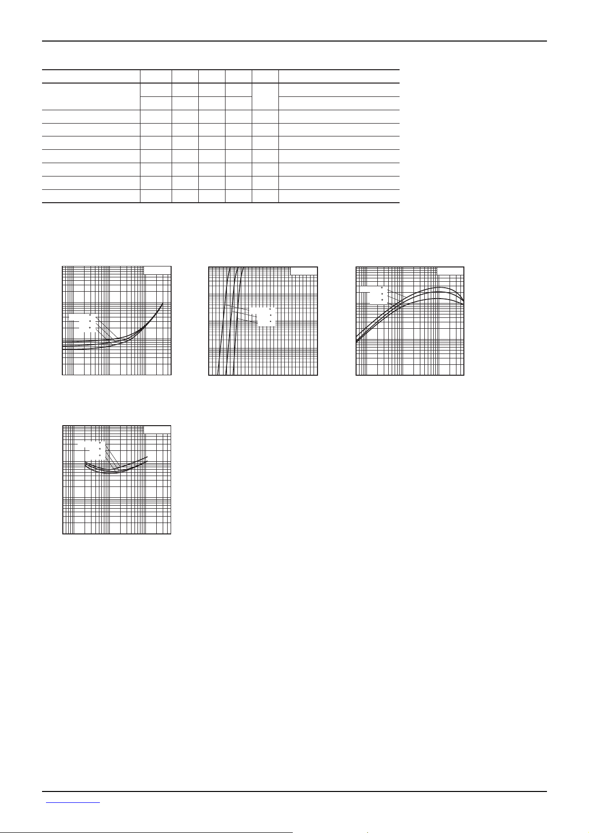
Fig.1 Input voltage vs. output current
(ON characteristics)
-1
-500m
V)
(
O (on)
OUTPUT VOLTAGE : V
Ta=100 C
-200m
-100m
-50m
-20m
-10m
-5m
-2m
-1m
-500∝
25 C
40 C
-1m
-2m -5m -10m -20m -50m-100m-200m-500m
OUTPUT CURRENT : I
Fig.4 Output voltage vs. output
current
VO= 0.3V
O
(
A)
O
(
A)
lO/lI=20
I(off)
I(on)
O(on)
I
I
O(off)
G
f
T
R
Min.
−
2.5
−
−
−
115
I
−
3.29
1
0.8
1
Typ. Max. Unit Conditions
−
0.5
−
−
60
300
−
1.4
−
0.5
−
−
260
4.7
1.0
-5m
-2m
A)
-1m
-500∝
-200∝
-100∝
-50∝
-20∝
-10∝
OUTPUT CURRENT : Io (
-5∝
-2∝
-1∝
−
6.11
1.2
Ta=100 C
-0.5 -1.0 -1.5 -2.0 -2.5 -3.00
INPUT VOLTAGE : V
MHz
CC
= 5V, IO= 100µA
V
V
O
= 0.3V, IO= 20mA
V
mV
I
O/II
= 100mA / 5mA
mA
I
= 5V
V
µA
V
CC
= 12V, VI=0V
−
O
= 2V, IO= 100mA
V
CE
= 10V, IE=−5mA, f=100MHz
V
kΩ
−−
VCC= 5V
25 C
40 C
I (off)
(
V)
Fig.2 Output current vs. input voltage
(OFF characteristics)
−
1k
500
I
Ta=100 C
200
25 C
40 C
100
50
20
10
5
DC CURRENT GAIN : G
2
1
-1m
-2m -5m -10m -20m -50m-100m-200m-500
-500∝
OUTPUT CURRENT : I
Fig.3 DC current gain vs. output
current
O
VO= 5V
(
A)
Data Sheet DTD543EE / DTD543EM
www.rohm.com
2/2
c
○
2009 ROHM Co., Ltd. All rights reserved.
2009.05 - Rev.B
 Loading...