ROHM DTD113EK Technical data

500mA / 50V Digital transistors
(with built-in resistors)
DTD113EK
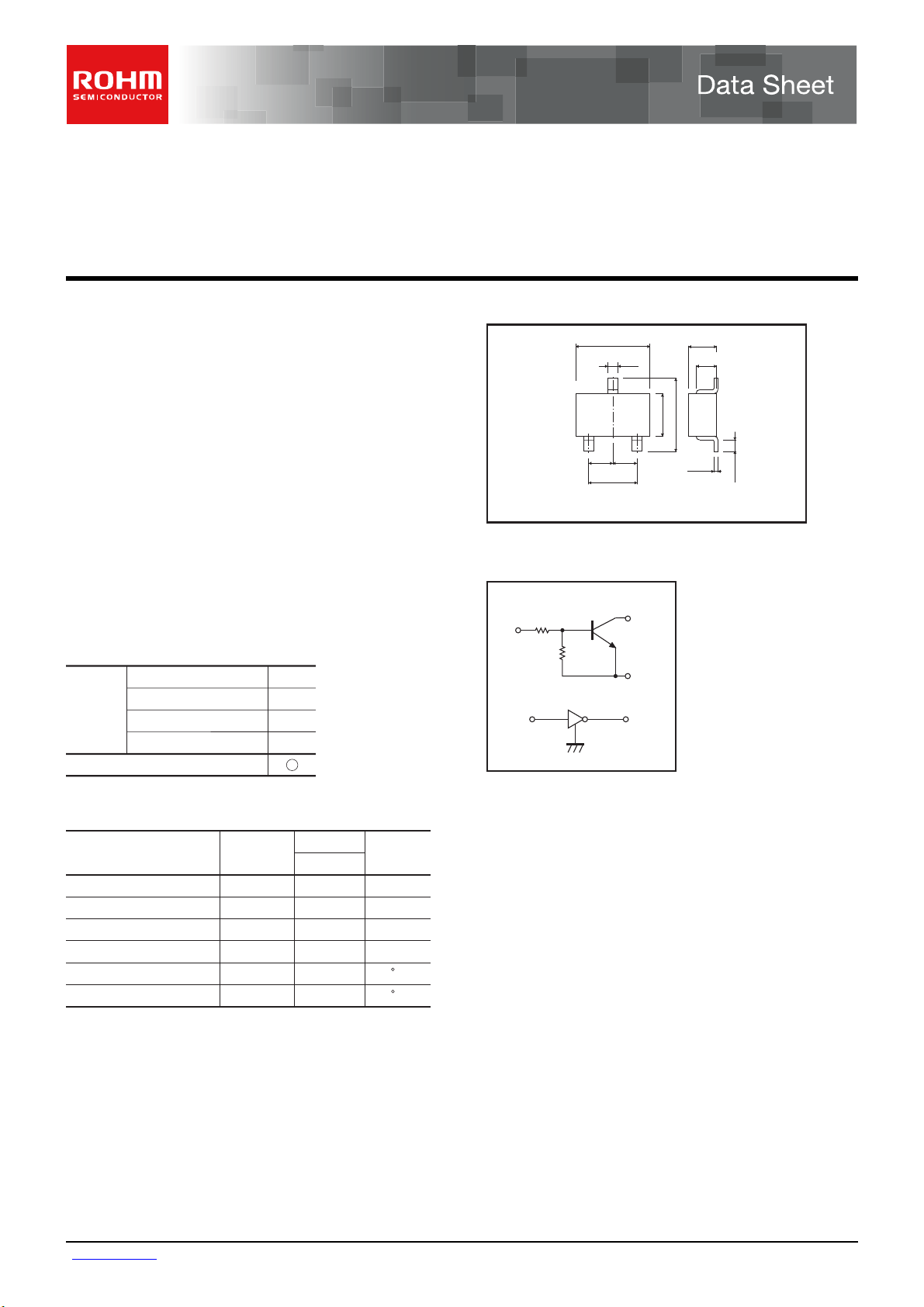
Applications Dimensions (Unit : mm)
Inverter, Interface, Driver
DTD113EK
Features
1) Built-in bias resistors enable the configuration of an inverter
circuit without connecting external input resistors (see
equivalent circuit).
2) The bias resistors consist of thin-film resistors with complete
isolation to allow negative biasing of the input. They also have
the advantage of almost completely eliminating parasitic
effects.
3) Only the on / off conditions need to be set for operation,
ROHM : SMT3
EIAJ : SC-59
making the device design easy.
Structure Inner circuit
NPN epitaxial planar silicon transistor
(Resistor built-in type)
R
Packaging specifications
Package
Packaging type
Code
Part No.
DTD113EK
Basic ordering unit (pieces)
SMT3
Taping
T146
3000
R1=R2=1.0kΩ
1
IN
R
2
IN
Absolute maximum ratings (Ta=25C)
Parameter Symbol
Supply voltage
Input voltage
Output current
Power dissipation
Junction temperature
Storage temperature
V
CC
V
C
I
Pd
Tj
Tstg
IN
Limits
DTD113EK
50
−10 to +10
500
200
150
−55 to +150
Unit
V
V
mA
mW
C
C
2.9
0.4
(3)
(2)
0.95 0.95
1.9
Each lead has same dimension
Abbreviated symbol : F21
OUT
GND
OUT
GND
1.1
0.8
1.6
2.8
(1)
0.15
0.3Min.
(1) GND
(2) IN
(3) OUT
www.rohm.com
1/2
c
○
2009 ROHM Co., Ltd. All rights reserved.
2009.06 - Rev.C

Electrical characteristics (Ta=25C)
Parameter Symbol
V
O
(A)
VI(on)
VO(on)
IO(off)
R2/R1
VO=0.3V
lO/lI=20
GI
R1
I(off)
II
fT
∗
Input voltage
Output voltage
Input current
Output current
DC current gain
Input resistance
Resistance ratio
Transition frequency
Characteristics of built-in transistor
∗
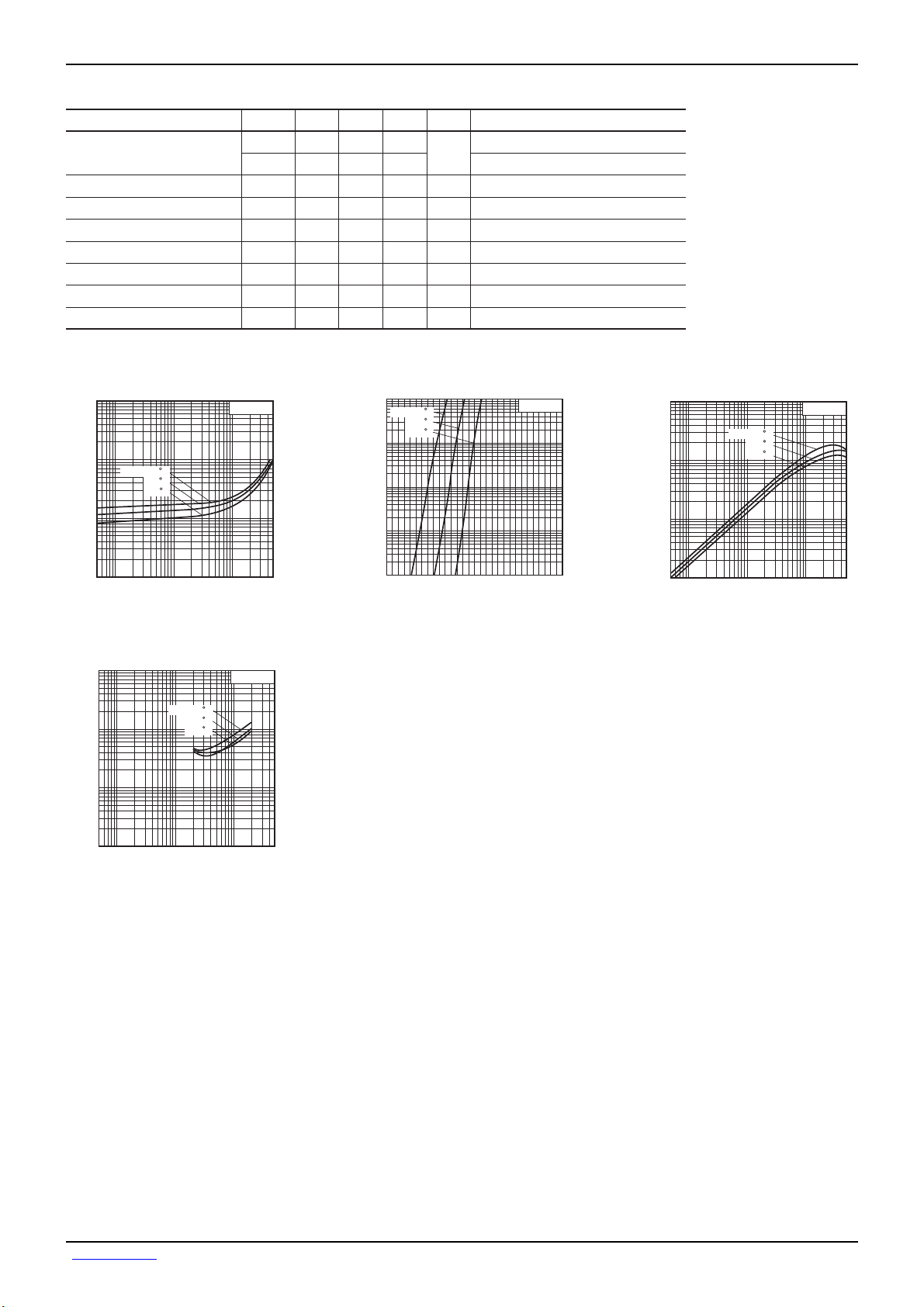
Electrical characteristic curves
100
50
20
(V)
I(on)
10
Ta= −40 C
5
2
1
500m
INPUT VOLTAGE : V
200m
100m
500μ 1m 2m 5m 10m 20m 50m100m 200m 500m
25 C
100 C
OUTPUT CURRENT : I
Fig.1 Input voltage vs. output current
(ON characteristics)
1
500m
200m
100m
50m
20m
10m
5m
OUTPUT VOLTAGE : VO(on) (V)
2m
1m
500 μ
1m 2m 5m 10m 20m 50m 500m100m200m
Ta=100 C
25 C
−40 C
OUTPUT CURRENT : IO (A)
Fig.4 Output voltage vs. output current
Min.
Typ. Max. Unit Conditions
−
−
33
0.7
0.8
0.5
3
−
−
−
0.1
0.3
−
−
7.2
−
−
0.5
−
−
1
1.3
1
1.2
−
200
OUTPUT CURRENT : Io (A)
10m
500μ
200μ
100μ
−
5m
Ta=100 C
25 C
2m
−40 C
1m
50μ
20μ
10μ
5μ
2μ
1μ
0.5 1.0 1.5 2.0 2.5 3.0 0
INPUT VOLTAGE : VI(off) (V)
V
CC=5V, IO=100μA
V
O=0.3V, IO=20mA
V
I
O/I
I
V
mA
μA
−
=50mA/2.5mA
V
I
=5V
CC=50V, VI=0V
V
O=5V, IO=50mA
V
kΩ
−−
CE=10V, IE= −50mA, f=100MHz
V
MHz
Fig.2 Output current vs. input voltage
(OFF characteristics)
VCC=5V
Data Sheet DTD113EK
−
1k
500
I
200
100
50
20
10
5
DC CURRENT GAIN : G
2
1
1m500μ 2m 5m 10m 20m 50m 500m100m200m
Ta=100 C
25 C
−40 C
OUTPUT CURRENT : I
Fig.3 DC current gain
vs. output current
O
(A)
VO=5V
www.rohm.com
2/2
c
○
2009 ROHM Co., Ltd. All rights reserved.
2009.06 - Rev.C
 Loading...