ROHM DTC614TU Technical data

DTC614TU / DTC614TK
Transistors
Digital transistors (built-in resistor)
DTC614TU / DTC614TK
zFeatures
In addition to the features of regular digital transistors.
1) Low saturation voltage, typically
V
CE (sat) =40mV at IC / IB=50mA / 2.5mA, makes these
transistors ideal for muting circuits.
2) These transistors can be used at high current levels,
I
C=600mA.
zStructure
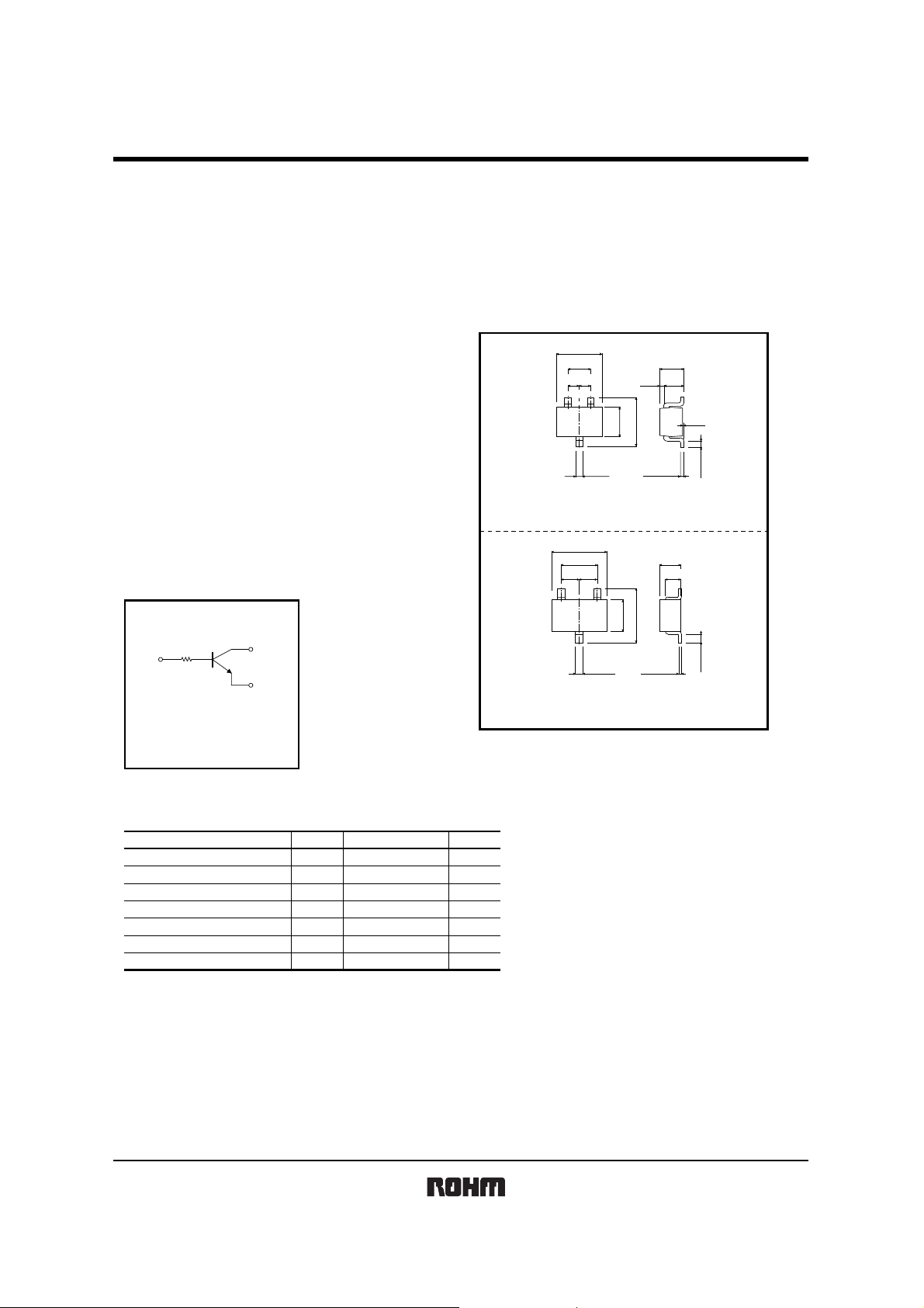
NPN digital transistor
(Built-in resistor type)
zEquivalent circuit
B
B : Base
C : Collector
E : Emitter
R
R=10kΩ
C
E
zAbsolute maximum ratings (Ta=25°C)
Parameter Symbol
Collector-base voltage
Collector-emitter voltage
Emitter-base voltage
Collector current
Collector power dissipation
Junction temperature
Storage temperature
V
CBO
V
CEO
V
EBO
I
C
C
Tj 150
Tstg
Limits
20
20
12
600
200P
−55 to +150
zExternal dimensions (Unit : mm)
2.0±0.2
1.3±0.1
0.65
0.65
(1)
(2)
±0.1
2.1±0.1
(3)
2.9±0.2
1.9±0.2
1.25
+0.1
0.3
−0
Abbreviated symbol : R04
0.950.95
(2)(1)
+0.2
−0.1
2.8±0.2
1.6
(3)
+0.1
0.4
−0.05
Abbreviated symbol : R04
0.2
Each lead has same dimensions
0.15
Each lead has same dimensions
Unit
V
V
V
mA
mW
°C
°C
UMT3
<SC-70>
(1) Emitter
(2) Base
(3) Collector
SMT3
<SC-59>
(1) Emitter
(2) Base
(3) Collector
0.15
0.9±0.1
0.7
±0.05
1.1
0.8±0.1
+0.1
−0.06
±0.1
+0.2
−0.1
0−0.1
0.1Min.
0.3Min.
Rev.A 1/2

Transistor
zElectrical characteristics (Ta=25°C)
Parameter Symbol Min. Typ. Max. Unit Conditions
Collector-base breakdown voltage
Collector-emitter breakdown voltage
Emitter-base breakdown voltage
BV
BV
BV
Collector cutoff current
Emitter cutoff current
Collector-emitter saturation voltage
V
DC current transfer ratio
Input resistance
Transition frequency
Output "ON" resistance
∗
Transition frequency of the device.
zPackaging specifications and hFE
Type
DTC614TU
DTC614TK
Package
Packaging type
Code
Basic ordering unit (pieces)
UMT3
Taping Taping
T106
3000
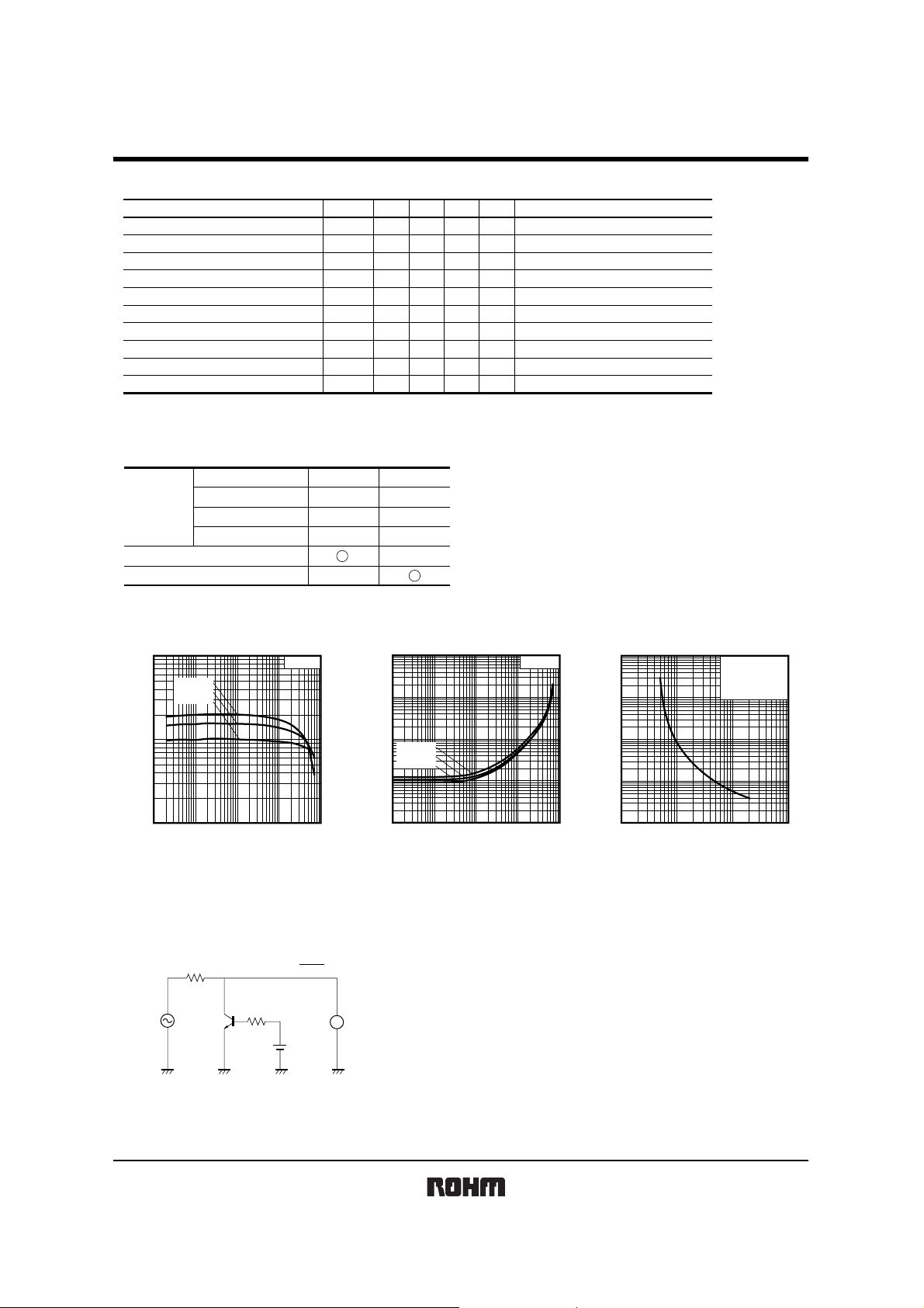
zElectrical characteristic curves
10000
FE
Ta=100°C
Ta=25°C
Ta= −40°C
VCE=5V
CBO
CEO
EBO
I
CBO
I
EBO
CE (sat)
FE
R
1
f
T
R
on
−
20
20
12
−−
−−
−
820
710
150
−
−
SMT3
T146
3000
−
10000
1000
−
−
−
40
−
0.9
− V
− V
− V
0.5 µA
0.5 µA
150 mV
2700 −
13 kΩ
− MHz
− Ω
DTC614TU / DTC614TK
=50µA
I
C
=1mA
I
C
=50µA
I
E
=20V
V
CB
V
=12V
EB
I
/ IB=50mA / 2.5mA
C
=5V, IC=50mAh
V
CE
−
V
=10V, IE= −50mA, f=100MHz
CE
VI=5V, R
IC / IB=20
=1kΩ, f=1KHz
L
1000
100
(Ω)
on
∗
Ta=25°C
f=1kHz
=1kΩ
R
L
hFE=250 (5V / 50mA)
1000
DC CURRENT GAIN : h
100
0.1 1 10 100 1000
COLLECTOR CURRENT : I
C
Fig.1 DC Current Gain vs.
Collector Current
(mA)
100
Ta=100°C
Ta=25°C
Ta= −40°C
10
COLLECTOR SATURATION
VOLTAGE : V
1
0.1 1 10 100 1000
COLLECTOR CURRENT : I
Fig.2 Collector-Emitter Saturation
Voltage vs. Collector Current
(mA)
C
10
1
ON RESISTANCE : R
0.1
0.1 1 10 100
INPUT VOLTAGE : V
Fig.3
"ON" resistance vs. Input Voltage
(V)
I
CE (sat) (mV)
zR
on measurement circuit
v
Input
v
i
100mV
(rms)
f=1kHz
RL=1kΩ
on
= ×R
R
v
I
vi−v
0
0
V
L
Output
v
0
Fig.4 Output "ON" resistance (Ron)
measurement circuit
Rev.A 2/2
 Loading...