

ROHM DTC123JUA, DTC123JSA, DTC123JKA, DTC123JE Datasheet
DTC123JE / DTC123JUA / DTC123JKA / DTC123JSA
Transistor
Digital transistors (built-in resistors)
DTC123JE / DTC123JUA / DTC123JKA / DTC123JSA
Features
!
1) Built-in bias resistors enable the
configuration of an inverter circuit
without connecting external input
resistors (see the equivalent
circuit).
2) The bias resistors consist of thinfilm resistors with complete
isolation to allow negative biasing
of the input. They also have the
advantage of almost completely
eliminating parasitic effects.
3) Only the on / off conditions need
to be set for operation, making
device design easy.
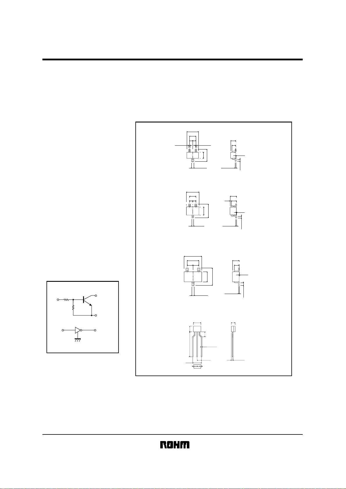
Structure
!!!!
NPN digital transistor
(Built-in resistor type)
Equivalent circuit
!!!!
R1
IN
R2
IN
OUT
GND
OUT
GND
External dimensions
!!!!
DTC123JE
ROHM : EMT3
DTC123JUA
ROHM : UMT3
EIAJ : SC-70
DTC123JKA
ROHM : SMT3
EIAJ : SC-59
DTC123JSA
(Units : mm)
1.6±0.2
1.0±0.1
0.50.5
+0.1
0.2
−
0.05
(1)
All terminals have same dimensions
(1)
All terminals have same dimensions
+0.1
0.2
−
0.05
(2)
0.8±0.1
1.6±0.2
(3)
+0.1
0.3
−
0.05
Abbreviated symbol : E42
2.0±0.2
1.3±0.1
0.65 0.65
(2)(1)
2.1±0.1
1.25±0.1
(3)
+0.1
0.3
−
0
Abbreviated symbol : E42
2.9±0.2
1.9±0.2
0.95
0.95
(2)
0.1
−
+0.2
2.8±0.2
1.6
(3)
+0.1
0.4
−
0.05
Abbreviated symbol : E42
4±0.2 2±0.2
3±0.2(15Min.)
3Min.
+0.15
0.45
−0.05
0.7±0.1
0.15±0.05
0.2
0.15±0.05
0.15
0.55±0.1
0.9±0.1
0.7±0.1
1.1
0.8±0.1
+0.1
−
0.06
+0.2
−
0.1
0~0.1
0~0.1
0.1Min.
0.1~0.4
0~0.1
0.3~0.6
(1) GND
(2) IN
(3) OUT
(1) GND
(2) IN
(3) OUT
(1) GND
(2) IN
(3) OUT
ROHM : SPT
EIAJ : SC-72
+0.4
2.5
−0.1
5
(1)
(2) (3)
+0.15
0.45
0.5
−0.05
(1) GND
(2) OUT
(3) IN

Transistor
DTC123JE / DTC123JUA / DTC123JKA / DTC123JSA
Absolute maximum ratings
!!!!
Parameter Symbol
V
V
I
C(Max.)
Pd
Tstg
CC
IN
I
O
Tj
Supply voltage
Input voltage
Output current
Power dissipation
Junction temperature
Storage temperature
Electrical characteristics
!!!!
Parameter Symbol
Input voltage
Output voltage
Input current
Output current
DC current gain
Input resistance
Resistance ratio
Transition frequency
*Transition frequency of the device
(Ta=25°C)
Limits(DTC123J )
E
UA KA SA
50
-5~+12
100
100
150 200 300
150
-55~+150
(Ta=25°C)
Min.
Typ. Max. Unit Conditions
1.1
80
1.54
17
-
-
-
0.1
-
-
-
-
-
-
2.2
21
250
-
V
I(off)
VI(on)
VO(on)
II
IO(off)
GI
R1
R2/R1
fT
Packaging specifications
!!!!
Unit
V
V
Part No.
mA
mW
˚C
DTC123JE
DTC123JUA
DTC123JKA
DTC123JSA
˚C
0.5
-
0.3
3.6
0.5
-
2.86
26
-
V
CC=5V, IO=100µA
V
O=0.3V, IO=5mA
V
I
O/II=5mA/0.25mA
V
V
mA
I=5V
µA
V
CC=50V, VI=0V
-
V
O=5V, IO=10mA
kΩ
-V
MHz
CE=10V, IE=-5mA, f=100MHz *
Package
UMT3EMT3 SMT3
SPT
Packaging type Taping Taping Taping Taping
Code
Basic ordering
unit (pieces)
TL
3000
-
-
---
T106
3000
T146
3000
-
-
-
-
TP
5000
-
-
-
-
Electrical characteristics curves
!!!!
100
50
20
(V)
I (on)
10
5
Ta=-40˚C
2
1
500m
INPUT VOLTAGE : V
200m
100m
100µ 200µ 500µ 1m 2m 5m 10m 20m 50m 100m
25˚C
100˚C
OUTPUT CURRENT : I
O
(A)
VO=0.3V
Fig.1 Input voltage vs. output current
(ON characteristics)
1
500m
(V)
200m
O (on)
100m
50m
20m
10m
5m
OUTPUT VOLTAGE : V
2m
1m
100µ 200µ 500µ 1m 2m 5m 10m 20m 50m 100m
Ta=100˚C
-40˚C
OUTPUT CURRENT : I
25˚C
O
lO/lI=20
(A)
Fig.4 Output voltage vs. output
current
10m
5m
2m
(A)
1m
500µ
200µ
100µ
50µ
20µ
10µ
OUTPUT CURRENT : Io
5µ
2µ
1µ
0 3.0
Ta=100˚C
25˚C
-40˚C
0.5 1.0 1.5 2.0 2.5
INPUT VOLTAGE : V
Fig.2 Output current vs. input voltage
(OFF characteristics)
I (off)
VCC=5V
(V)
1k
VO=5V
500
I
DC CURRENT GAIN : G
Ta=100˚C
200
100
50
20
10
5
2
1
100µ 200µ 500µ 1m 2m 5m 10m 20m 50m 100m
25˚C
-40˚C
OUTPUT CURRENT : I
O
(A)
Fig.3 DC current gain vs. output
current
 Loading...