

r
r
100mA / 50V Digital transistors
(with built-in resistors)
DTC115TM / DTC115TE / DTC115TUA / DTC115TKA
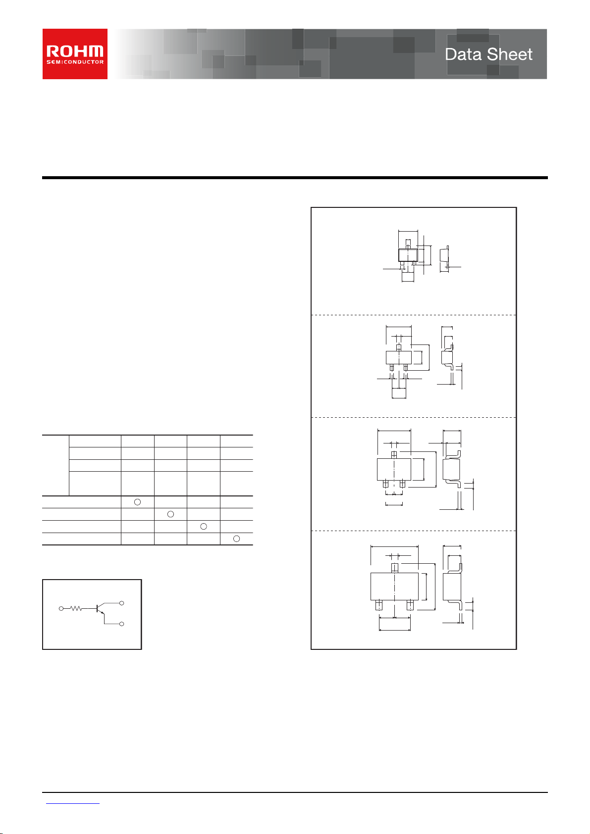
Applications Dimensions (Unit : mm)
Inverter, Interface, Driver
Features
1) Built-in bias resistors enable the configuration of an
inverter circuit without connecting external input
resistors.
2) The bias resistors consist of thin-film resistors with
complete isolation to allow negative biasing of the
input, and parasitic effects are almost completely
eliminated.
3) Only the on / off conditions need to be set for
operation, making the device design easy.
4) Higher mounting densities can be achieved.
Structure
NPN epitaxial planar silicon transistor
(Resistor built-in type)
Packaging specifications
Package
Packaging type
Code
Basic ordering
unit (pieces)
Part No.
DTC115TM
DTC115TE
DTC115TUA
DTC115TKA
VMT3
T2L
8000
−
−
−
TapingTaping Taping Taping
3000
TL
−
−
−
UMT3EMT3 SMT3
T106
3000
T146
3000
−
−
−
−
−
−
Inner circuit
B
R
E : Emitter
C : Collector
B : Base
1
C
E
R1=100kΩ
DTC115TM
ROHM : VMT3
DTC115TE
ROHM : EMT3
DTC115TUA
ROHM : UMT3
EIAJ : SC-70
DTC115TKA
ROHM : SMT3
EIAJ : SC-59
1.2
0.32
(3)
(2)
(1)
0.22
0.40.4
0.8
Abbreviated symbol : 09
1.6
0.3
(3)
(2)
0.2
(1)
0.5
0.5
1.0
Abbreviated symbol : 09
2.0
0.3
(3)
(1)
(2)
0.65
0.65
1.3
Abbreviated symbol : 09
2.9
0.4
(3)
(2)
0.95 0.95
1.9
Abbreviated symbol : 09
0.2
1.2
0.8
0.13
0.2
0.5
0.7
0.55
1.6
0.8
0.2
0.15
0.2
2.1
1.25
0.15
1.6
2.8
(1)
0.15
(1) Base
(2) Emitter
(3) Collector
(1) Emitter
0.1Min.
(2) Base
(3) Collector
0.9
0.7
0.1Min.
(1) Emitter
(2) Base
(3) Collecto
1.1
0.8
0.3Min.
(1) Emitter
(2) Base
(3) Collecto
www.rohm.com
1/2
c
○
2011 ROHM Co., Ltd. All rights reserved.
2011.11 - Rev.C
Absolute maximum ratings (Ta=25C)
Collector-base voltage
Collector-emitter voltage
Emitter-base voltage
Collector current
Collector power
dissipation
Junction temperature
Storage temperature
Electrical characteristics (Ta=25C)
Collector-base breakdown voltage
Collector-emitter breakdown voltage
Emitter-base breakdown voltage
Collector cutoff current
Emitter cutoff current
Collector-emitter saturation voltage
DC current
Input resistance
Transition frequency
Characteristics of built-in transistor.
∗
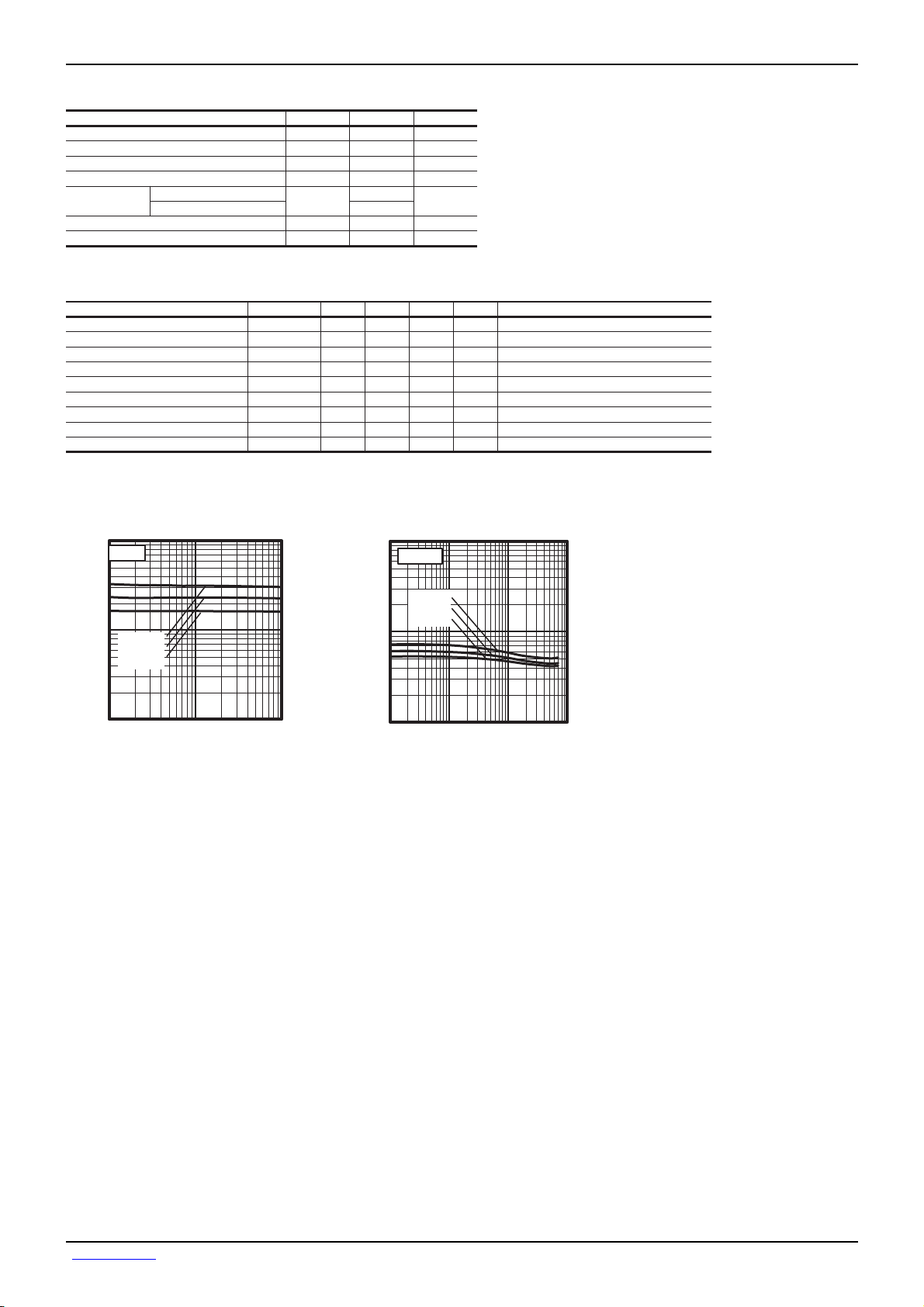
Electrical characteristics curves
1000
EF
h : NIAG TNERRUC CD
100
Parameter Symbol
V
CBO
V
CEO
V
EBO
I
DTC115TM / DTC115TE
DTC115TUA / DTC115TKA
C
Pc
Tj
Tstg
Parameter Symbol Min. Typ. Max. Unit Conditions
BV
CBO
BV
CEO
BV
EBO
I
CBO
I
EBO
V
transfer ratio
VCE=5V
Ta=100ºC
25ºC
-40ºC
CE(sat)
h
FE
R
1
f
T
∗
50
50
5
−
−
−
100
70
−
: EGATLOV NOITARUTAS ROTCELLOC
)V(
V
Limits
50
50
5
100
150
200
150
−55 to +150
−
−
−
−
−
−
250
100
250
1
)
tas(EC
0.1
−
−
−
0.5
0.5
0.3
600
130
−
IC/IB=20/1
Ta=10 0ºC
25ºC
-40ºC
Unit
mA
mW
˚C
˚C
Data Sheet DTC115TM / DTC115TE / DTC115TUA / DTC115TKA
V
V
V
I
V
C
=
50μA
V
I
C
=
1mA
V
I
E
=
μA
μA
kΩ
MHz
50μA
V
CB
=
50V
V
EB
=
I
I
C/IB
C
=
1mA, V
4V
=
1mA/0.1mA
CE
=
5V
V
−
−
CE
=
10V, I
E
=−
V
5mA, f=100MHz
10
0.1 1 10
COLLECTOR CURRENT : IC (mA)
Fig 1. DC Current Gain vs. Collector Current
0.01
0.01 0.1 1 10
OUTPUT CURRENT : IO (mA)
Fig 2. Collector Voltage vs.
Collector Saturation Voltage.
www.rohm.com
2/2
c
○
2011 ROHM Co., Ltd. All rights reserved.
2011.11 - Rev.C

Notes
Notice
www.rohm.com
© 2011 ROHM Co., Ltd. All rights reserved.
Thank you for your accessing to ROHM product informations.
More detail product informations and catalogs are available, please contact us.
ROHM Customer Support System
http://www.rohm.com/contact/
R1120A
 Loading...