


DTC115E series
NPN 100mA 50V Digital Transistors (Bias Resistor Built-in Transistors)
Datasheet
llOutline
Parameter Value
VMT3
EMT3F
V
CC
50V
I
C(MAX.)
100mA
R
1
100kΩ
DTC115EM DTC115EEB
R
2
100kΩ
(SC-105AA) (SC-89)
EMT3
UMT3
llFeatures
1) Built-In Biasing Resistors, R1 = R2 = 100kΩ
2) Built-in bias resistors enable the configuration of
an inverter circuit without connecting external
input resistors (see inner circuit) .
3) The bias resistors consist of thin-film resistors
with complete isolation to allow negative biasing
of the input. They also have the advantage of
completely eliminating parasitic effects.
4) Only the on/off conditions need to be set
for operation, making the circuit design easy.
5) Complementary PNP Types: DTA115E series
6) Lead Free/RoHS Compliant.
DTC115EE DTC115EUA
SOT-416(SC-75A) SOT-323(SC-70)
SMT3
DTC115EKA
SOT-346(SC-59)
llInner circuit
llApplication
Switching circuit, Inverter circuit, Interface circuit,
Driver circuit
llPackaging specifications
Part No. Package
Package
size
Taping
code
Reel size
(mm)
Tape width
(mm)
Basic
ordering
unit.(pcs)
Marking
DTC115EM VMT3 1212 T2L 180 8 8000 29
DTC115EEB EMT3F 1616 TL 180 8 3000 29
DTC115EE EMT3 1616 TL 180 8 3000 29
DTC115EUA UMT3 2021 T106 180 8 3000 29
DTC115EKA SMT3 2928 T146 180 8 3000 29
www.rohm.com
© 2012 ROHM Co., Ltd. All rights reserved.
1/9
20121023 - Rev.001

DTC115E series
Datasheet
llAbsolute maximum ratings (T
a
= 25°C)
Parameter Symbol Values Unit
Supply voltage
V
CC
50 V
Input voltage
V
IN
-10 to 40 V
Output current
I
O
20 mA
Collector current
I
C(MAX)
*1
100 mA
Power dissipation
DTC115EM
P
D
*2
150
mW
DTC115EEB 150
DTC115EE 150
DTC115EUA 200
DTC115EKA 200
Junction temperature
T
j
150 ℃
Range of storage temperature
T
stg
-55 to +150 ℃
llElectrical characteristics (T
a
= 25°C)
Parameter Symbol Conditions
Values
Unit
Min. Typ. Max.
Input voltage
V
I(off)
VCC = 5V, IO = 100μA - - 0.5
V
V
I(on)
VO = 0.3V, IO = 1mA
3 - -
Output voltage
V
O(on)
IO / II = 5mA / 0.25mA
- 0.1 0.3 V
Input current
I
I
VI = 5V
- - 0.15 mA
Output current
I
O(off)
VCC = 50V, VI = 0V
- - 0.5 μA
DC current gain
G
I
VO = 5V, IO = 5mA
82 - - -
Input resistance
R
1
- 70 100 130 kΩ
Resistance ratio
R2/R
1
- 0.8 1 1.2 -
Transition frequency
f
T
*1
VCE = 10V, IE = -5mA,
f = 100MHz
- 250 - MHz
*1 Characteristics of built-in transistor
*2 Each terminal mounted on a reference footprint
www.rohm.com
© 2012 ROHM Co., Ltd. All rights reserved.
2/9
20121023 - Rev.001
DTC115E series
Datasheet
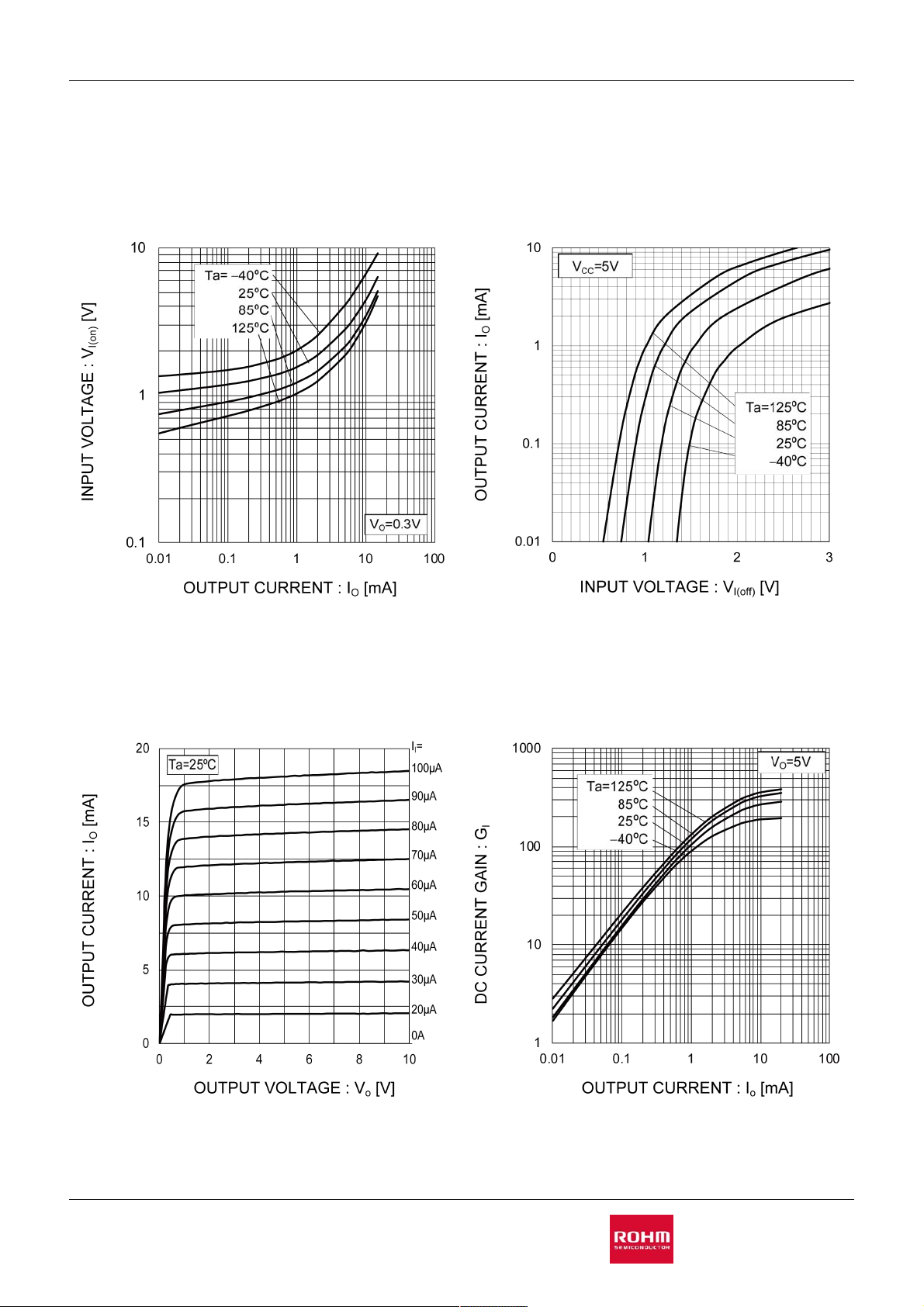
llElectrical characteristic curves (T
a
=25°C)
Fig.1 Input voltage vs. output current
(ON characteristics)
Fig.2 Output current vs. input voltage
(OFF characteristics)
Fig.3 Output current vs. output voltage Fig.4 DC current gain vs. output current
www.rohm.com
© 2012 ROHM Co., Ltd. All rights reserved.
3/9
20121023 - Rev.001

DTC115E series
Datasheet
llElectrical characteristic curves (T
a
=25°C)
Fig.5 Output voltage vs. output current
www.rohm.com
© 2012 ROHM Co., Ltd. All rights reserved.
4/9
20121023 - Rev.001
 Loading...