

Page 1
Data Sheet
100mA/50V Digital transistors(with built-in resistors)
DTC043ZM / DTC043ZEB / DTC043ZUB
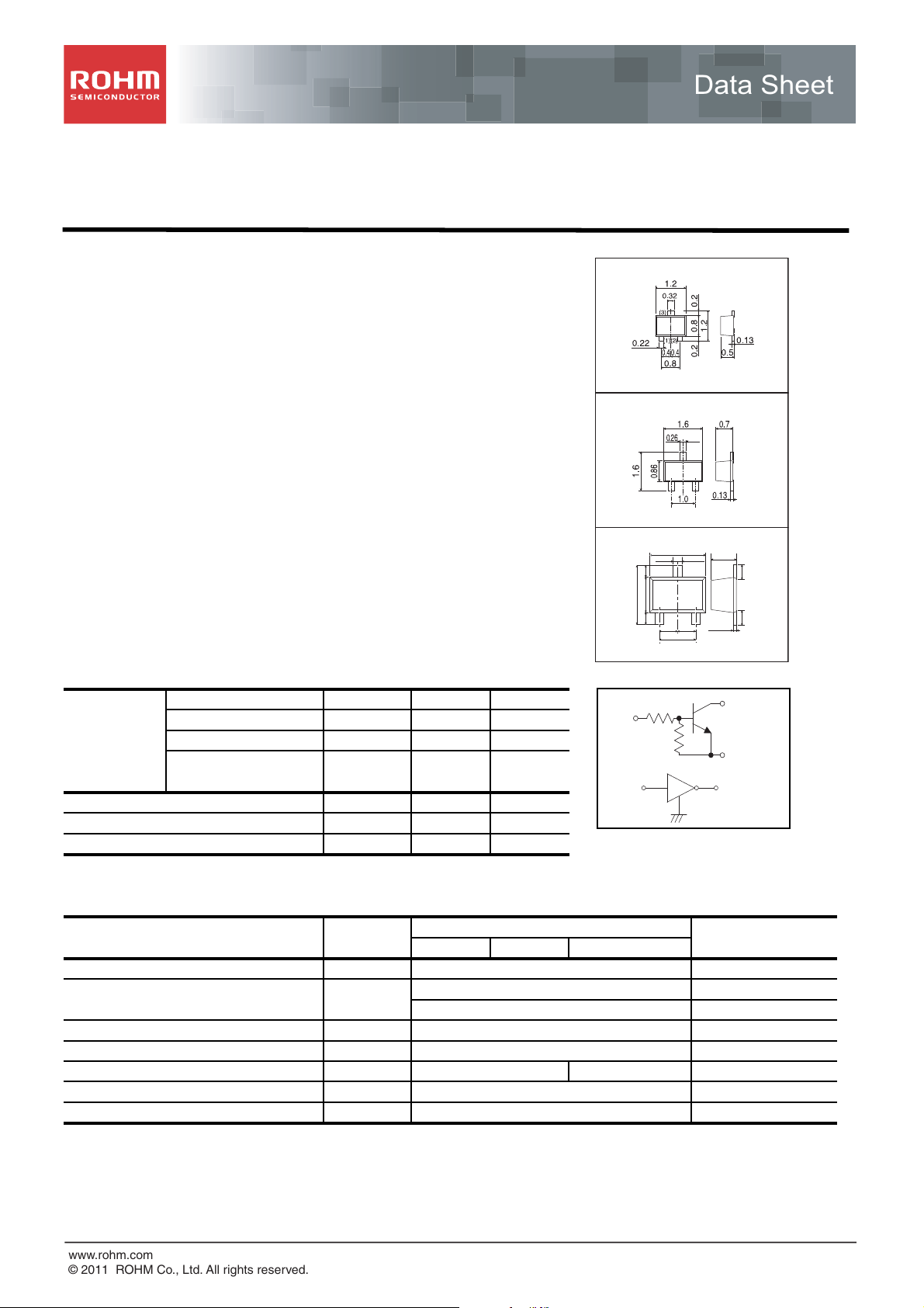
Features Dimensions (Unit : mm)
1) Built-in bias resistors enable the configuration of
an inverter circuit without connecting external input resistors.
(See Equivalent circuit)
2) The bias resistors consist of thin-film resistors with complete
isolation to allow negative biasing of the input.
They also have the advantage of almost completely
eliminating parasitic effects.
3) Only the on/off conditions need to be set for operation,
making the device design easy.
VMT3
Abbreviated symbol : 42
EMT3F
(3)
Structure
NPN epitaxial planar silicon transistor
(Resistor built-in type)
Applications
Inverter, Interface, Driver
Packaging specifications and h
Package VMT3 EMT3F
FE
UMT3F
Equivalent circuit
Packaging Type Taping Taping Taping
Type
DTC043ZM
DTC043ZEB
DTC043ZUB - -
Code T2L TL
Basic ordering
unit (pieces)
8000 3000 3000
○
-○
TL
--
-
○
Absolute maximum (Ta=25C)
Parameter Symbol
Supply voltage
Input voltage
Collector current *1
Output current
Power dissipation *2
V
V
I
C(max)
I
P
CC
IN
O
D
Limits(DTC043Z□)
MEB UB
50 V
30 V
-5 V
100 mA
100 mA
150 200
Junction temperature Tj 150
Range of storage temperature Tstg -55 to +150
*1 Characteristics of built-in transistor
*2 Each terminal mounted on a reference land
(1) (2)
Abbreviated symbol : 42
UMT3F
0.32
0.4250.425
2.1
1.25
Abbreviated symbol : 42
R
IN
IN
=4.7k, R2=47k
R
1
2.0
(3)
(1) (2)
0.65 0.65
1.3
1
R
2
0.9
0.530.53
0.13
OUT
GND
OUT
GND
Unit
mW
C
C
www.rohm.com
© 2011 ROHM Co., Ltd. All rights reserved.
1/2
2011.09 - Rev.A
Page 2

www.rohm.com
© 2011 ROHM Co., Ltd. All rights reserved.
Data Sheet
DTC043ZM / DTC043ZEB / DTC043ZUB
Electrical characteristics (Ta=25C)
Parameter Min. Typ. Test Conditions
Input voltage
Output voltage - 0.05
Input current - -
Output current - -
DC current gain 80 -
Transition frequency * - 250
Input resistance 3.29 4.7
Resistance ratio 8 10
* Characteristics of built-in transistor
Electrical characteristics curves
Symbol Max. Unit
V
V
V
I
R
I(off)
I(on)
O(on)
I
I
O(off)
G
f
T
R
2/R1
I
1
--
1.1 -
0.5 V
-V
0.15 V
1.8 mA
500 nA
--
- MHz
6.11
k
12 -
VCC=5V / IO=100uA
VO=0.3V / IO=5mA
IO=5mA / II=0.5mA
VI=5V
VCC=50V / VI=0V
V
=10V / IO=5mA
O
VCE=10V /IE=-5mA
f=100MHz
(mA)
O
OUTPUT CURRENT : I
10
1
Ta=125ºC
0.1
0.01
0.001
0 0.5 1 1.5 2 2.5 3
INPUT VOLTAGE : V
Ta=75ºC
Ta=25ºC
Ta=-40ºC
100
(V)
I(on)
10
1
INPUT VOLTAGE : V
0.1
Ta=-40ºC
Ta=25ºC
Ta=75ºC
Ta=125ºC
0.1 1 10 100
OUTPUT CURRENT : I
VO=0.3V
(mA)
O
Fig.1 Input Voltage vs. Output Current Fig.2 Input Voltage vs. Output Current
(ON characteristics) (OFF characteristics)
I
1000
100
Ta=125ºC
Ta=75ºC
Ta=25ºC
Ta=-40ºC
VO=10V
(V)
O(on)
1
0.1
I(off)
VCC=5V
(V)
IO/II=10
10
DC CURRENT GAIN : G
1
0.1 1 10 100
OUTPUT CURRENT : I
Fig.3 DC Current Gain vs. Output Current Fig.4 Output Voltage vs. Output Current
(mA)
O
2/2
0.01
OUTPUT VOLTAGE : V
0.001
0.1 1 10 100
Ta=125ºC
Ta=75ºC
Ta=25ºC
Ta=-40ºC
OUTPUT CURRNET : I
(mA)
O
2011.09 - Rev.A
Page 3

Notes
Notice
www.rohm.com
© 2011 ROHM Co., Ltd. All rights reserved.
Thank you for your accessing to ROHM product informations.
More detail product informations and catalogs are available, please contact us.
ROHM Customer Support System
http://www.rohm.com/contact/
R1120A
 Loading...