ROHM DTC023JM, DTC023JEB, DTC023JUB Technical data

www.rohm.com
©2011 ROHM Co., Ltd. All rights reserved.
100mA/50V Digital transistors(with built-in resistors)
DTC023JM / DTC023JEB / DTC023JUB
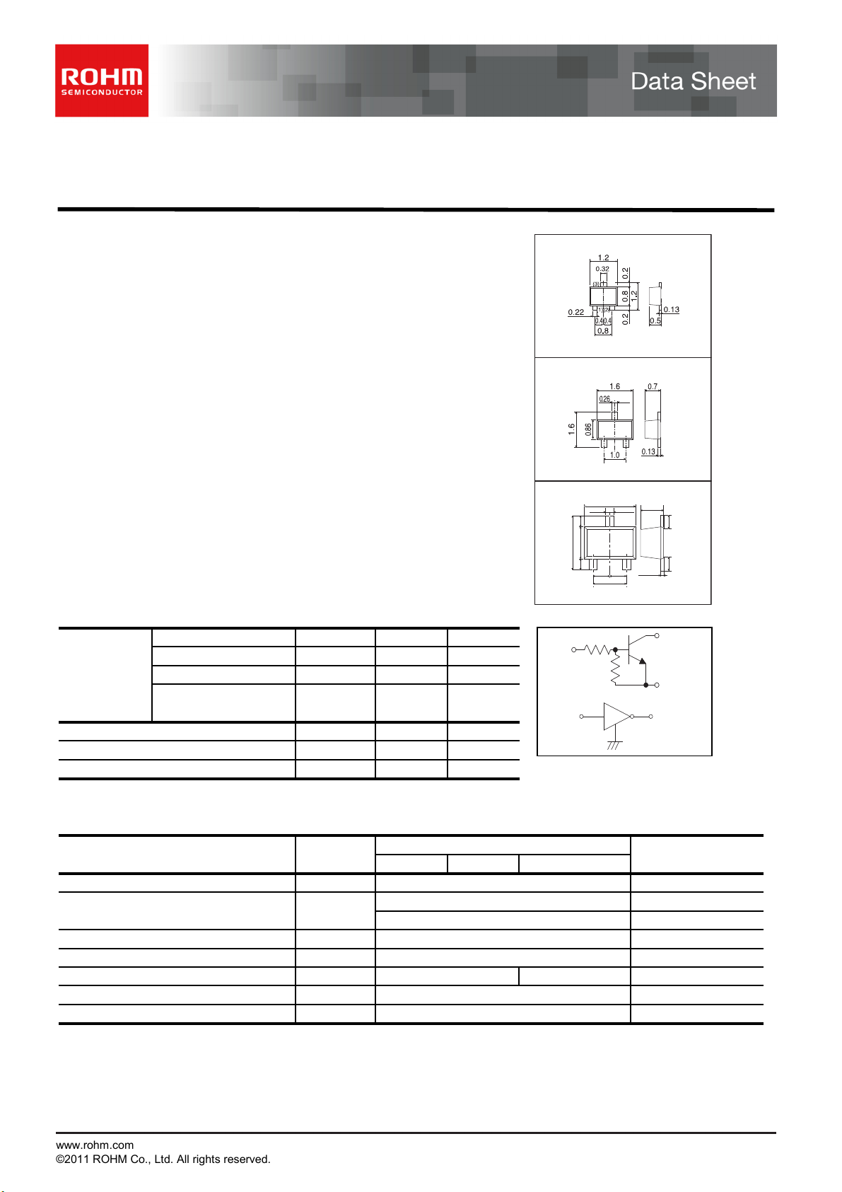
Features Dimensions (Unit : mm)
1) Built-in bias resistors enable the configuration of
an inverter circuit without connecting external input resistors.
(See equivalent circuit)
2) The bias resistors consist of thin-film resistors with complete
isolation to allow negative biasing of the input.
They also have the advantage of almost completely
eliminating parasitic effects.
3) Only the on/off conditions need to be set for operation,
making the device design easy.
VMT3
Abbreviated symbol : 46
EMT3F
(3)
Structure
NPN epitaxial planar silicon transistor
(Resistor built-in type)
Applications
Inverter, Interface, Driver
Packaging specifications and h
Package VMT3 EMT3F
FE
UMT3F
Equivalent circuit
Packaging Type Taping Taping Taping
Type
DTC023JM
DTC023JEB
DTC023JUB - -
Code T2L TL
Basic ordering
unit (pieces)
8000 3000 3000
○
-○
TL
--
-
○
Absolute maximum (Ta=25C)
Parameter Symbol
Supply voltage
Input voltage
Collector current *1
Output current
Power dissipation *2
V
V
I
C(max)
I
P
CC
IN
O
D
Limits(DTC023J□)
MEB UB
50 V
12 V
-5 V
100 mA
100 mA
150 200
Junction temperature Tj 150
Range of storage temperature Tstg -55 to +150
*1 Characteristics of built-in transistor
*2 Each terminal mounted on a reference land
UMT3F
(1) (2)
Abbreviated symbol : 46
2.0
0.32
(3)
0.4250.425
2.1
1.25
(1) (2)
0.65 0.65
1.3
Abbreviated symbol : 46
R
1
IN
R
2
IN
=2.2k,R2=47k
R
1
0.9
0.530.53
0.13
OUT
GND
OUT
GND
Unit
mW
C
C
1/2
2011.08 - Rev.A

DTC023JM / DTC023JEB / DTC023JUB
Electrical characteristics (Ta=25C)
Parameter Min. Typ. Test Conditions
Input voltage
Output voltage - 0.05
Input current - -
Output current - -
DC current gain 80 -
Transition frequency * - 250
Input resistance 1.54 2.2
Resistance ratio 17 21
* Characteristics of built-in transistor
Electrical characteristics curves
Symbol Max. Unit
V
V
V
I
R
I(off)
I(on)
O(on)
I
I
O(off)
G
f
T
R
2/R1
I
1
--
1.1 -
0.5 V
-V
0.15 V
3.6 mA
500 nA
--
- MHz
2.86
k
26 -
VCC=5V / IO=100uA
VO=0.3V / IO=5mA
IO=5mA / II=0.5mA
VI=5V
VCC=50V / VI=0V
V
=10V / IO=5mA
O
=10V /IE=-5mA
V
CE
f=100MHz
Data Sheet
(mA)
O
OUTPUT CURRENT : I
10
1
0.1
0.01
0.001
0 0.5 1 1.5 2 2.5 3
INPUT VOLTAGE : V
Ta=125ºC
Ta=75ºC
Ta=25ºC
Ta=-40ºC
I(off)
VCC=5V
(V)
100
(V)
I(on)
10
Ta=-40ºC
Ta=25ºC
Ta=75ºC
Ta=125ºC
1
INPUT VOLTAGE : V
0.1
0.1 1 10 100
OUTPUT CURRENT : I
VO=0.3V
(mA)
O
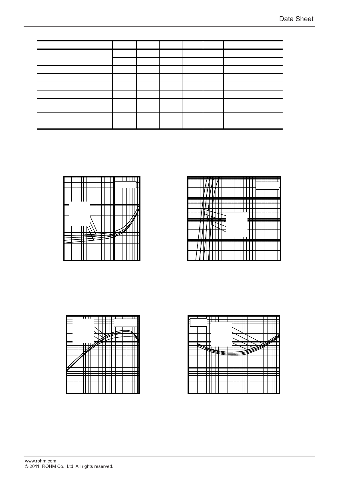
Fig.1 Input Voltage vs. Output Current Fig.2 Input Voltage vs. Output Current
(ON characteristics) (OFF characteristics)
I
1000
100
Ta=125ºC
Ta=75ºC
Ta=25ºC
Ta=-40ºC
VO=10V
(V)
O(on)
0.1
1
IO/II=10
Ta=125ºC
Ta=75ºC
Ta=25ºC
Ta=-40ºC
10
DC CURRENT GAIN : G
1
0.1 1 10 100
OUTPUT CURRENT : I
Fig.3 DC Current Gain vs. Output Current Fig.4 Output Voltage vs. Output Current
www.rohm.com
© 2011 ROHM Co., Ltd. All rights reserved.
(mA)
O
OUTPUT VOLTAGE : V
2/2
0.01
0.001
0.1 1 10 100
OUTPUT CURRNET : I
O
(mA)
2011.08 - Rev.A
 Loading...