ROHM DTB143TK Technical data

Transistors
-500mA / -40V Digital transistors (with built-in resistor)
DTB143TK
zApplic ations
Inverter, Interface, Driver
zFeatures
1) Built-in bias resistors enable the configuration of an
inverter circuit without connecting external input
resistors (see equivalent circuit).
2) The bias resistors consist of thin-film resistors with
complete isolation to allow positive bia sing o f the inpu t.
They also have the advantage of almost completely
eliminating parasitic effects.
3) Only the on / off conditions need to be set for
operation, making the device design easy .
zStructure
PNP epitaxial planar silicon transistor
(Resistor built-in type)
zPackaging specifications
Part No.
DTB143TK
Package
Packaging type
Code
Basic ordering
unit (pieces)
SMT3
Taping
T146
3000
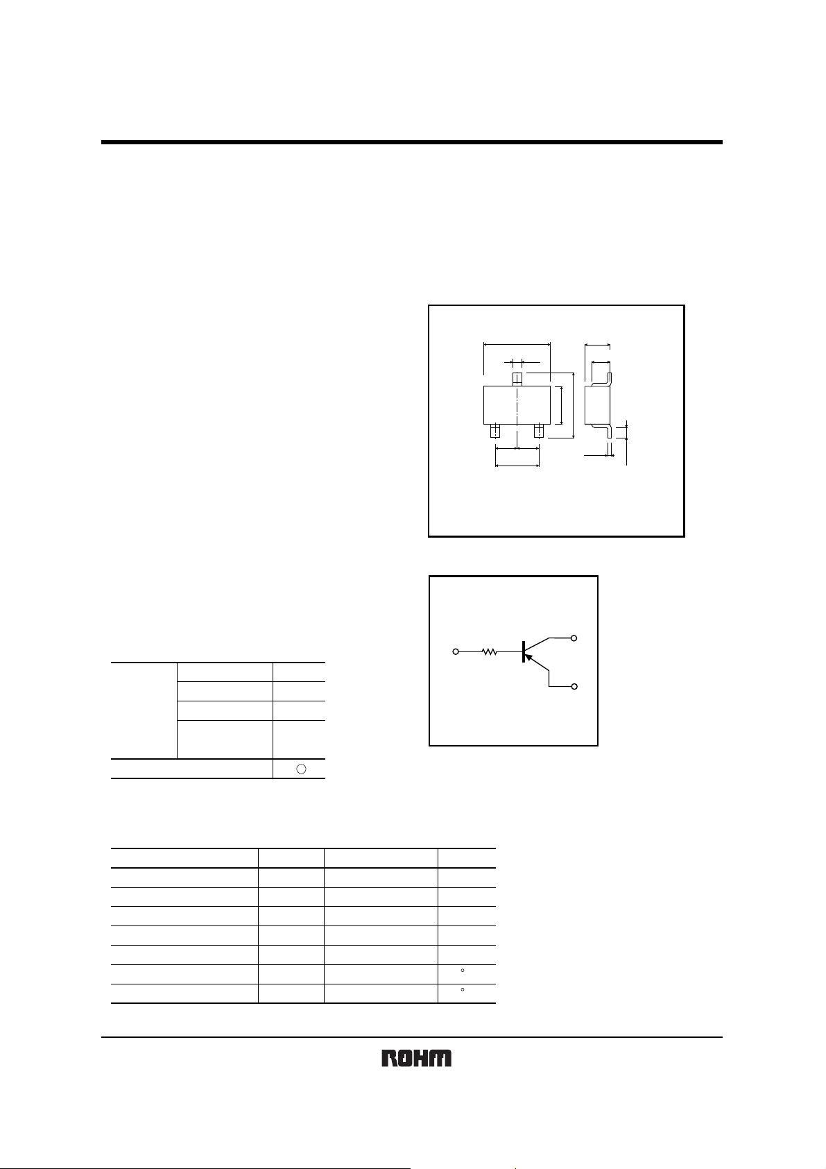
zExternal dimensions (Unit : mm)
2.9
0.4
(3)
1.6
ROHM : SMT3
EIAJ : SC-59
(2)
0.95 0.95
(1)
1.9
Each lead has same dimension
Abbreviated symbol : F93
zEquivalent circ uit
B
B : Base
C : Collector
E : Emitter
R1=4.7kΩ
R
1
DTB143TK
1.1
0.8
2.8
0.15
0.3Min.
(1) Emitter
(2) Base
(3) Collector
C
E
zAbsolute maximum ratings (Ta=25°C)
Unit
V
V
V
mA
mW
C
C
Collector-base voltage
Collector-emitter voltage
Emitter-base voltage
Collector current
Collector power dissipation
Junction temperature
Storage temperature
V
CBO
CEO
V
V
EBO
I
P
Tj
Tstg
LimitsParameter Symbol
−50
−40
−5
C
C
−500
200
150
−55 to +150
Rev.B 1/2

Transistors
m
F
nt
)
m
t
zElectrical characteristics (Ta=25°C)
DTB143TK
Parameter Symbol
Collector-base breakdown voltage
Collector-emitter breakdown voltage
Emitter-base breakdown voltage
Collector cutoff current
Emitter cutoff current
Collector-emitter saturation voltage
DC current transfer ratio
Input resistance
Transition frequency
Characteristics of built-in transistor
∗
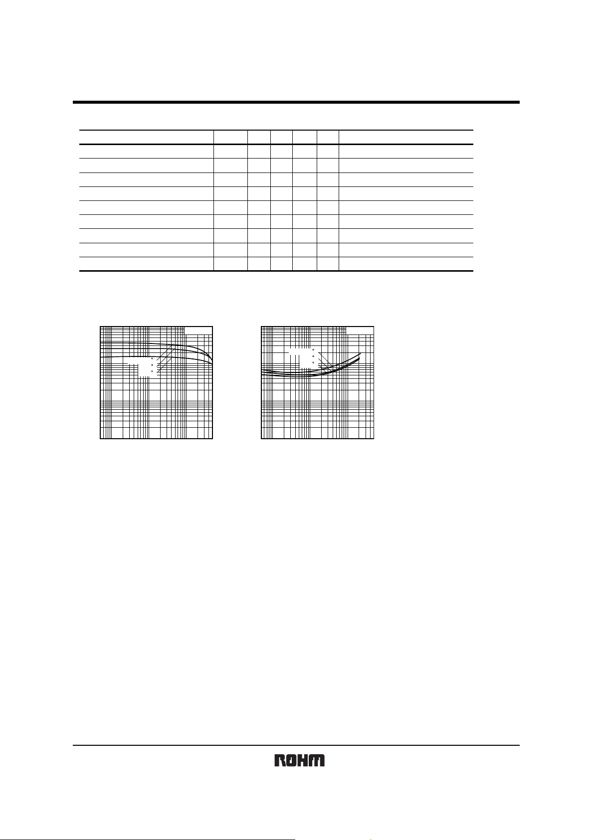
zElectrical characteristic curves
1k
500
FE
200
100
50
20
10
5
DC CURRENT GAIN : h
2
1
Ta=100 C
25 C
−40 C
-1m-0.5m -2m -5m -10m -20m -50m -100m -200m -500
COLLECTOR CURRENT : I
ig.1 DC current gain vs. collectorcurre
V
CE
= −
5V
A)
C
(
Typ. Max. Unit Conditions
Min.
CBO
BV
BV
CEO
BV
EBO
I
CBO
I
EBO
V
CE(sat)
h
FE
R
1
f
T
∗
(V
CE (sat)
COLLECTOR SATURATION VOLTAGE : V
−
−50
−
−40
−
−5
−
−
−
−
−
−
100
250
3.29
4.7
−
200
-1
-500m
-200m
-100m
-50m
-20m
-10m
-5m
-2m
-1m
Ta=100 C
-1m-0.5m -2m -5m -10m -20m -50m -100m -200m -500
COLLECTOR CURRENT : I
Fig.2Collector-emitter saturation
voltage vs. collector curren
−
VI
C
= −50µA
−
−
−0.5
−0.5
−0.3
600
6.11 −
−
25 C
−40 C
V
V
µA
µA
V
−
kΩ
MHz
C
= −1mA
I
I
E
= −50µA
CB
= −50V
V
EB
= −4V
V
I
C/IB
= −50mA/−2.5mA
V
CE
= −5V, IC= −50mA
V
CE
= −10V, IE=50mA, f=100MHz
lC/lB=20
C
(A)
Rev.B 2/2
 Loading...