

DTA124EE / DTC124EUA / DTA124EKA /
Transistor
DTA124ECA / DTA124ESA
Digital transistors (built-in resistors)
DTA124EE / DTA124EUA / DTA124EKA /
DTA124ECA / DTA124ESA
Features
!
1) Built-in bias resistors enable the
configuration of an inverter circuit
without connecting external input
resistors (see the equivalent
circuit).
2) The bias resistors consist of thinfilm resistors with complete
isolation to allow positive biasing
of the input. They also have the
advantage of almost completely
eliminating parasitic effects.
3) Only the on / off conditions need
to be set for operation, making
device design easy.
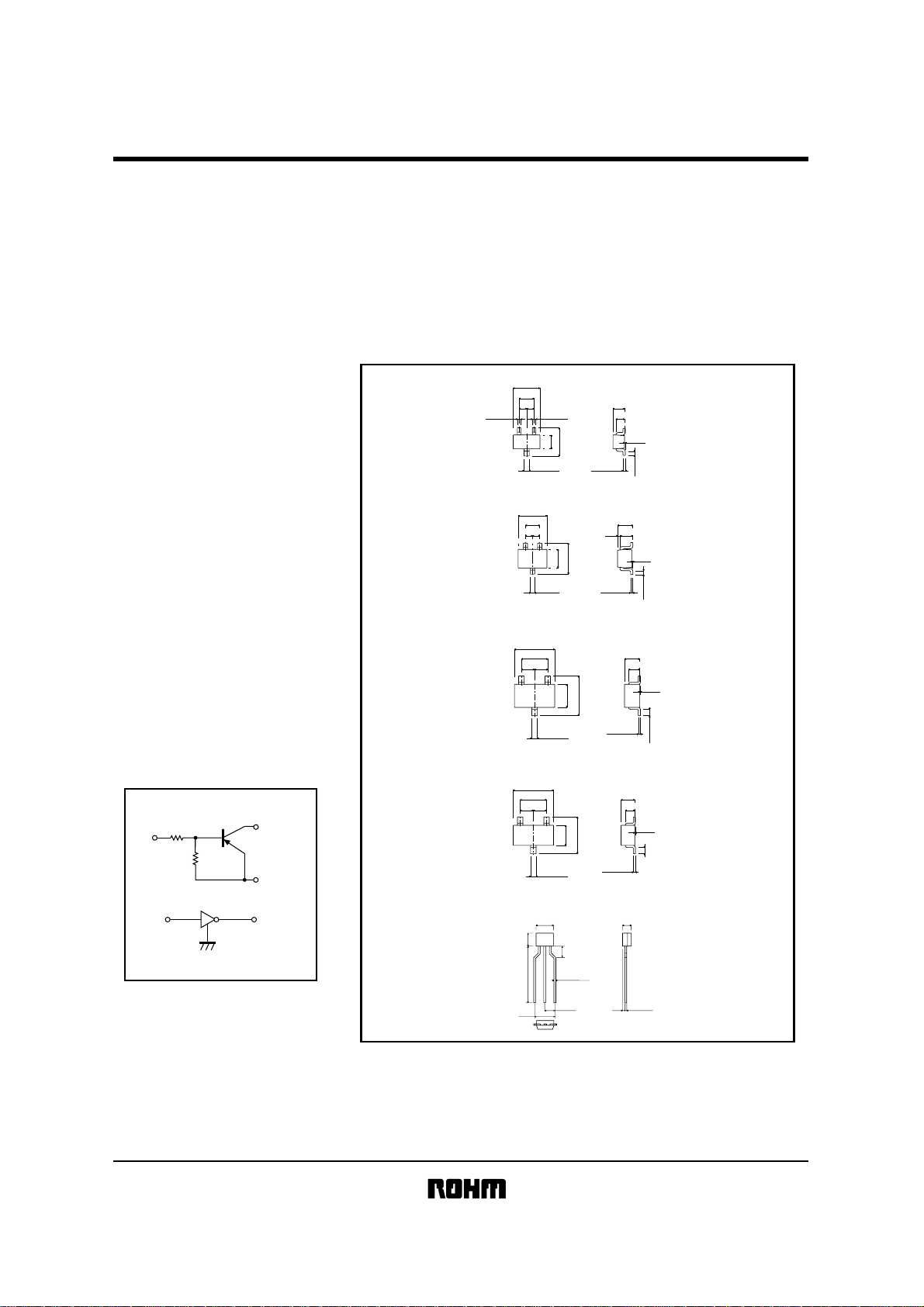
Structure
!
PNP digital transistor
(Built-in resistor type)
Equivalent circuit
!
R1
IN
R2
IN
OUT
GND(+)
OUT
GND(+)
External dimensions
!
DTA124EE
ROHM : EMT3
DTA124EUA
ROHM : UMT3
EIAJ : SC-70
DTA124EKA
ROHM : SMT3
EIAJ : SC-59
DTA124ECA
ROHM : SST3
DTA124ESA
ROHM : SPT
EIAJ : SC-72
(Units : mm)
1.6±0.2
1.0±0.1
0.50.5
+0.1
0.2
−0.05
All terminals have same dimensions
All terminals have same dimensions
All terminals have same dimensions
+0.1
0.2
−0.05
(1)
(2)
0.8±0.1
1.6±0.2
(3)
+0.1
0.3
−0.05
Abbreviated symbol : 15
2.0±0.2
1.3±0.1
0.65 0.65
(2)(1)
2.1±0.1
1.25±0.1
(3)
+0.1
0.3
−0
Abbreviated symbol : 15
2.9±0.2
1.9±0.2
0.95
0.95
(2)
(1)
−0.1
+0.2
2.8±0.2
1.6
(3)
+0.1
0.4
−0.05
Abbreviated symbol : 15
2.9±0.2
1.9±0.2
0.95
0.95
(2)
(1)
0.1
−
+0.2
1.3
2.4±0.2
(3)
+0.1
0.4
−0.05
Abbreviated symbol : 15
4±0.2 2±0.2
0.2(15Min.)
±
3
3Min.
+0.15
0.45
−0.05
+0.4
2.5
−
0.1
5
(1)
(2) (3)
0.15±0.05
0.2
0.15±0.05
0.15
0.7±0.1
0.55±0.1
0.15
+0.1
−0.06
0.5
0.9±0.1
0.7±0.1
1.1
+0.1
−0.06
0.95
0.45±0.1
0~0.1
+0.2
−0.1
0.8±0.1
+0.2
−0.1
0.45
0.1Min.
0~0.1
0~0.1
0.2Min.
+0.15
−0.05
0.1~0.4
0~0.1
0.3~0.6
(1) GND
(2) IN
(3) OUT
(1) GND
(2) IN
(3) OUT
(1) GND
(2) IN
(3) OUT
(1) GND
(2) IN
(3) OUT
(1) GND
(2) OUT
(3) IN

DTA124EE / DTC124EUA / DTA124EKA /
Transistor
DTA124ECA / DTA124ESA
Absolute maximum ratings
!
Parameter Symbol
Supply voltage
Input voltage
Output current
Power dissipation
Junction temperature
Storage temperature
Electrical characteristics
!
I
E
V
CC
IN
V
I
O
C(Max.)
150 200 300
Pd
Tj
Tstg
(Ta=25°C)
Parameter Symbol
V
Input voltage
Output voltage
I(off)
VI(on)
VO(on)
Input current
Output current
DC current gain
Input resistance
Resistance ratio
Transition frequency
IO(off)
GI
R1
R2/R1
fT
* Transition frequency of the device
Electrical characteristics curves
!
-100
-50
-20
(V)
I (on)
-10
Ta= −40˚C
-5
-2
-1
-500m
INPUT VOLTAGE : V
-200m
-100m
-100µ
25˚C
100˚C
-1m -10m -100m
-200µ -2m -20m-500µ -5m -50m
OUTPUT CURRENT : I
O
(A)
VO=-0.3V
Fig.1 Input voltage vs. output current
(ON characteristics)
(Ta=25°C)
II
!Packaging specifications
Limits(DTA124E )
UA KA CA SA
-50
-40~+10
-30
-100
150
-55~+150
Min.
Typ. Max. Unit Conditions
-
-
--
-3
-0.1
-
-
-
-
-
-
56
22
15.4
1
0.8
250
--
-10m
-5m
-2m
(A)
-1m
-500µ
-200µ
-100µ
-50µ
-20µ
-10µ
OUTPUT CURRENT : Io
-5µ
-2µ
-1µ
0 -3.0
Fig.2 Output current vs. input voltage
Unit
V
V
Part No.
DTA124EE
mA
DTA124EUA
mW
DTA124EKA
DTA124ECA
˚C
DTA124ESA
˚C
-0.5
-0.3
-0.36
-0.5
-
28.6
1.2
VCC=-
5V
Ta=
100˚C
25
˚C
-40
˚C
-0.5 -1.0 -1.5 -2.0 -2.5
INPUT VOLTAGE : V
CC=-5V, IO=-100µA
V
V
V
O=-0.2V, IO=-5mA
I
O/II=-10mA/-0.5mA
V
V
mA
I=-5V
µA
V
CC=-50V, VI=0V
V
-
O=-5V, IO=-5mA
kΩ
-V
MHz
CE=-10V, IE=5mA, f=100MHz *
(OFF characteristics)
Package
Package type Taping Taping Taping Taping Taping
Code
Basic ordering
unit (pieces)
UMT3EMT3 SMT3 SST3
T106
TL
3000
-
-
---
----
3000
-
-
T146
3000
-
--
-
1k
I (off)
(V)
500
I
200
100
50
20
10
5
DC CURRENT GAIN : G
2
1
-100µ -1m -10m -100m
-200µ -2m -20m-500µ -5m -50m
Ta=100˚C
25˚C
-40˚C
OUTPUT CURRENT : I
Fig.3 DC current gain vs. output
current
T116
3000
SPT
TP
5000
-
-
-
-
-
-
VO=-
5V
O
(A)
-1
-500m
(V)
-200m
O(on)
-100m
-50m
-20m
-10m
-5m
OUTPUT VOLTAGE : V
-2m
-1m
-100µ -1m -10m -100m-200µ -2m -20m-500µ -5m -50m
Ta=100
˚C
25
˚C
-40
˚C
OUTPUT CURRENT : I
O
(A)
Fig.4 Output voltage vs. output
current
lO/lI=20

 Loading...