

DAN217
Diodes
Switching diode
DAN217
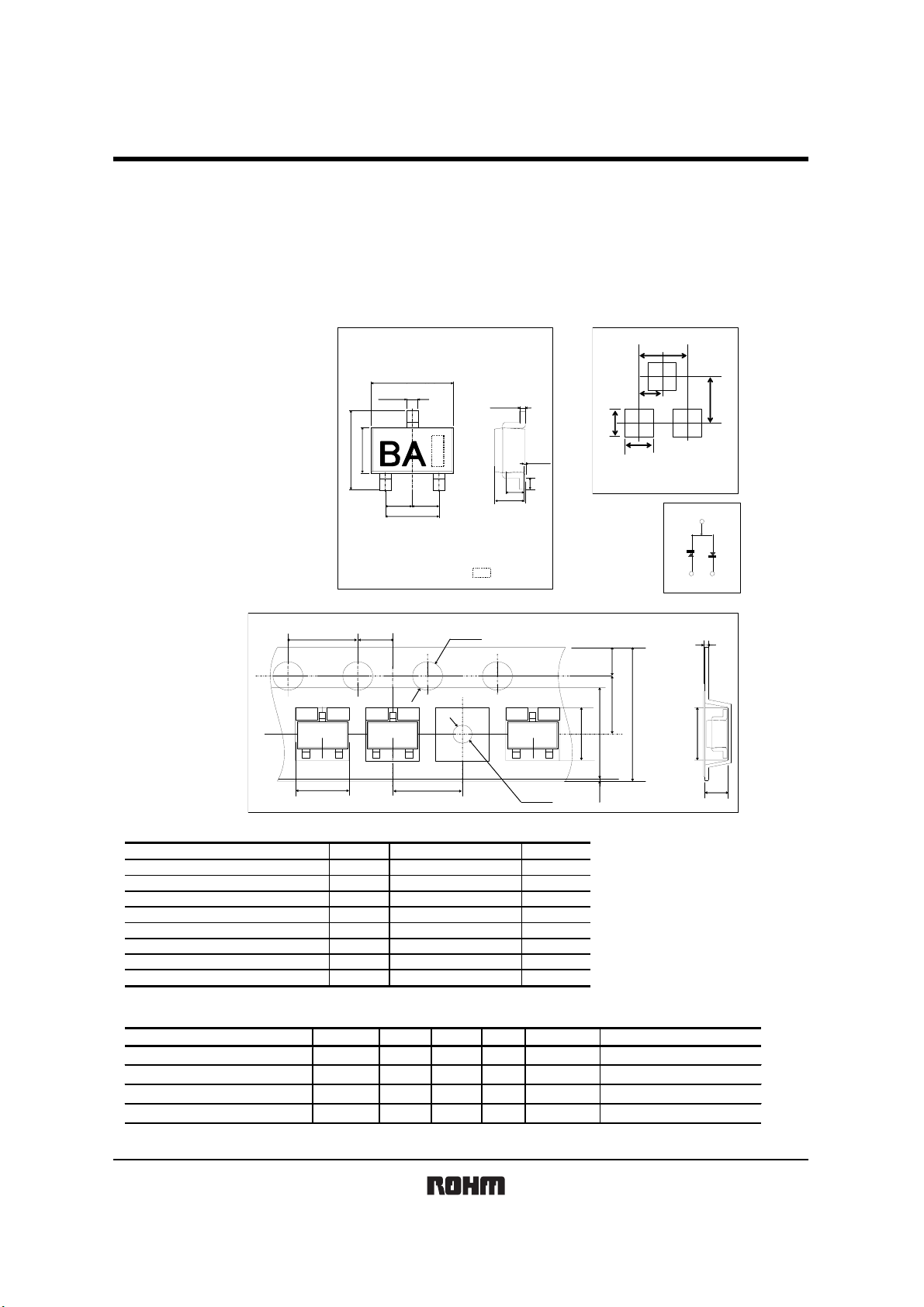
zApplication zExternal dimensions (Unit : mm) zLand size figure (Unit : mm)
Ultra high speed switching
+0.2
-0.1
1.6
2.9±0.2
各リードとも
+0.1
Each lead has s am e dimension
同寸法
0.4
-0.05
(2) (1)
0.95 0.95
1.9±0.2
+0.1
0.15
(3)
-0.06
0.8±0.1
1.1±0.2
0.01
ROH M : SMD3
JEDEC :S0T-346
JEITA : SC-59
weekcode
0~0.1
0.3~0.6
SMD3
zFeatures
1) Small mold type. (SMD3)
2) High reliability.
2.8±0.2
zConstruction
Silicon epitaxial planar zStructure
zT aping specifications (Unit : mm)
4.0±0.1
2.0±0.05
φ1.5±0.1
0
3.2±0.1
5.5±0.2
3.2±0.1
4.0±0.1
φ1.05MIN
0~0.5
zAbsolute maximum ratings (Ta=25°C)
everse voltage (repetitive peak)
R
Reverse voltage (DC)
orward current (Single)
F
verage rectified forward cur rent (Single)
A
urge current (t=1us
S
ower dissipation
P
unction temperature
J
torage temperature
S
Param e ter
)
Sym bol Unit
V
RM
V
R
I
FM
Io mA
I
surge
Pd m W
Tj
Tstg
Limits
80
80
300
100
4
200
150
-55 to +150
V
V
mA
A
℃
℃
zElectrical characteristics (Ta=25°C)
Parameter
Forward voltag e
Reverse current
Capacitance between termi nals
Reverse recovery time
Symbol Min. Typ. Max. Unit
V
F
I
R
--1.2V
--0.1µA
Ct - - 3.5 pF
trr - - 4 ns
I
F
V
V
V
1.9
0.95
1.0MIN.
0.8MIN.
0.3±0.1
1.75±0.1
3.5±0.05
8.0±0.2
3.2±0.1
1.35±0.1
Conditions
=100mA
=70V
R
=6V , f=1MHz
R
=6V , IF=5mA , RL=50
R
2.4
Ω
Rev.B 1/2
Diodes
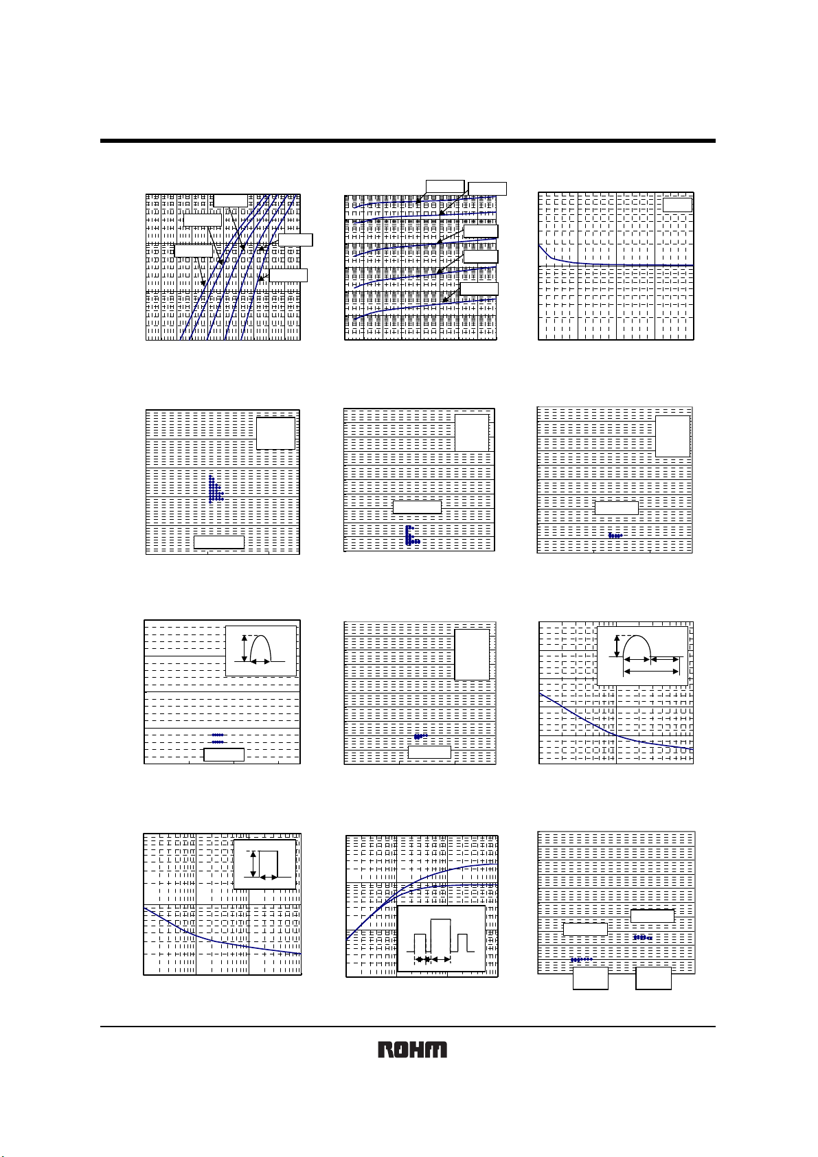
zElectrical characteristic curves (Ta=25°C)
100
)
IF(mA
10
NT:
RD C
1
FORWA URRE
Ta=75℃
Ta=125℃
Ta=150℃
Ta=-25℃
Ta=25℃
10000
1000
100
REVERSE CURRENT:IR(nA)
0.1
DAN217
Ta=150℃
10
1
Ta=125℃
Ta=75℃
Ta=25℃
Ta=-25℃
CAPACITANCE BETWEEN
10
1
TERMINALS:Ct(pF)
f=1MHz
0.1
0 100 200 300 400 500 600 700 800 900 100
FORWARD VO LTAGE:VF(mV)
VF-IF CHARACTERISTICS
950
940
930
920
910
FORWARD VO LTAGE:VF(mV)
900
20
15
10
PEAK SURGE
5
FORWARD CURRENT:IFSM(A)
0
AVE:921.7mV
VF DISPERSION MAP
AVE:3.50A
IFSM DISRESION M AP
Ifsm
Ta=25℃
IF=100mA
n=30pcs
1cyc
8.3ms
0.01
0
0 1020304050607080
REVERSE VOLTAGE:VR(V)
VR-IR CHARACTERISTICS
100
90
80
70
60
50
40
30
20
REVERSE CURRENT:IR(nA)
10
0
10
9
8
7
6
5
4
3
2
RESERVE RECOVERY TIME:trr(ns)
1
0
AVE:9.655nA
IR DISPERSION MAP
AVE:1.93ns
trr DISPERSION M AP
Ta=25℃
VR=80V
n=10pcs
Ta=25℃
VR=6V
IF=5mA
RL=50Ω
n=10pcs
0.1
0 5 10 15 20
REVERSE VOLTAGE:VR(V)
VR-Ct CHARACTERISTICS
10
8.3ms
1cyc
Ta=25℃
VR=6V
f=1MHz
n=10pcs
8.3ms
9
8
7
6
5
4
3
TERMINALS:Ct(pF)
CAPACITANCE BETWEEN
2
1
0
5
4
3
2
PEAK SURGE
1
FORWARD CURRENT:IFSM(A)
0
110100
AVE:1.17pF
Ct DISPERSION M AP
Ifsm
NUMBER OF CYCLES
IFSM-CYCLE CHARACTERISTICS
100
10
PEAK SURGE
FORWARD CURRENT:IFSM(A)
1
0.1 1 10 100
TIME:t(ms)
IFSM-t CHARACTERISTICS
Ifsm
t
1000
100
ガラスエポキシ基板実装時
TRANSIENT
10
THAERMAL IMPEDANCE:Rth (℃/W )
1
0.001 0.1 10 1000
Mounted on epoxy board
IM=1mA IF=10mA
IM=100mA IF=10A
time
1ms
1ms
300us
300us
TIME:t(s)
Rth-t CHARACTERISTICS
time
10
9
8
7
6
5
4
ELECTROSTATIC
DISCHARG E TEST ESD( KV)
AVE:0.97kV
3
2
1
0
C=200pF
R=0Ω
ESD DISPERSION M AP
AVE:2.54kV
C=100pF
R=1.5kΩ
Rev.B 2/2

Appendix
No technical content pages of this document may be reproduced in any form or transmitted by any
means without prior permission of ROHM CO.,LTD.
The contents described herein are subject to change without notice. The specifications for the
product described in this document are for reference only. Upon actual use, therefore, please request
that specifications to be separately delivered.
Application circuit diagrams and circuit constants contained herein are shown as examples of standard
use and operation. Please pay careful attention to the peripheral conditions when designing circuits
and deciding upon circuit constants in the set.
Any data, including, but not limited to application circuit diagrams information, described herein
are intended only as illustrations of such devices and not as the specifications for such devices. ROHM
CO.,LTD. disclaims any warranty that any use of such devices shall be free from infringement of any
third party's intellectual property rights or other proprietary rights, and further, assumes no liability of
whatsoever nature in the event of any such infringement, or arising from or connected with or related
to the use of such devices.
Upon the sale of any such devices, other than for buyer's right to use such devices itself, resell or
otherwise dispose of the same, no express or implied right or license to practice or commercially
exploit any intellectual property rights or other proprietary rights owned or controlled by
ROHM CO., LTD. is granted to any such buyer.
Products listed in this document are no antiradiation design.
Notes
The products listed in this document are designed to be used with ordinary electronic equipment or devices
(such as audio visual equipment, office-automation equipment, communications devices, electrical
appliances and electronic toys).
Should you intend to use these products with equipment or devices which require an extremely high level of
reliability and the malfunction of with would directly endanger human life (such as medical instruments,
transportation equipment, aerospace machinery, nuclear-reactor controllers, fuel controllers and other
safety devices), please be sure to consult with our sales representative in advance.
About Export Control Order in Japan
Products described herein are the objects of controlled goods in Annex 1 (Item 16) of Export Trade Control
Order in Japan.
In case of export from Japan, please confirm if it applies to "objective" criteria or an "informed" (by MITI clause)
on the basis of "catch all controls for Non-Proliferation of Weapons of Mass Destruction.
Appendix1-Rev1.1

 Loading...