

1
Memory ICs
Non-volatile electronic potentiometer
BU9831 / BU9831F
The BU9831 / BU9831F is a non-volatile electronic potentiometer with an internal 2k bit EEPROM. The resistance
value can be set by means of serial communications, and because the product contains an internal memory, conditions can be retained.
In addition, the 2k bit memory capacity enables digital data to be stored in the memory.
•
Absolute maximum ratings (Ta = 25°C)
Applied voltage
Power
dissipation
BU9831
BU9831F
Pd
Storage temperature
Operating temperature
Input voltage
∗
1 Reduced by 5.0mW for each increase in Ta of 1°C over 25°C.
∗
2 Reduced by 3.5mW for each increase in Ta of 1°C over 25°C.
VCC
Parameter Symbol
Tstg
Topr
—
– 0.3 ~ + 7.0
Limits
– 65 ~ + 125
– 20 ~ + 85
– 0.3 ~ V
CC + 0.3
mW
V
Unit
°C
°C
V
Wiper current
I
W
± 1.0 mA
500
∗
1
350
∗
2
•
Applications
Portable LCD backlight adjustment devices for notebook computers, and other sound adjustment devices for sets
•
Features
1) Internal 2k bit EEPROM
2) 100kΩ (1kΩ×100 steps) electronic potentiometer
3) Data in memory is automatically read when power supply is turned on, and resistance value is set.
4) Resistance value can be set using serial communications.
5) Low current consumption
When operating: 3mA (max.)
In standby mode: 200µA (max.)
•
Recommended operating conditions
Power supply voltage
Power supply voltage for writing Vccwr
VCC
Parameter Symbol
V
V
Unit
2.7 ~ 5.5
Limits
2.8 ~ 5.5
Input voltage V
IN V 0 ~ VCC
Voltage at resistor ends VRHL V 0 ~ VCC
Wiper pin voltage VW V 0 ~ VCC
2
Memory ICs BU9831 / BU9831F
•
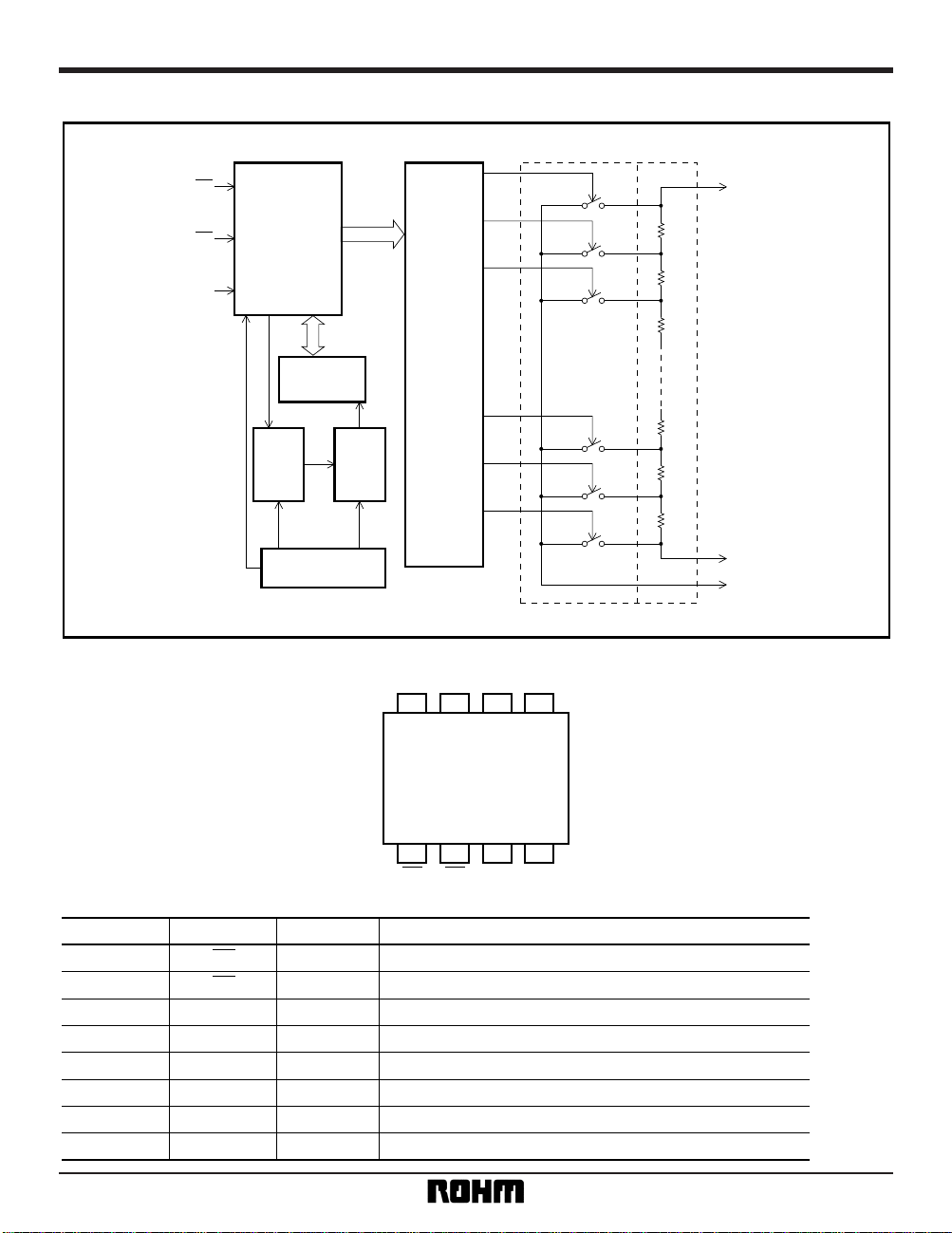
Block diagram
Command decode
Control
Timing Counter
EEPROM
Array
Wiper
decoder
Transistor
switch
Register
array
VW
VL
VH
High
voltage
generator
Write
Disable
Power supply
voltage detector
7bit
16bit
SK
DIO
CS
•
Pin assignments
CS SK DIO GND
VCC VH VW VL
BU9831
1234
8765
•
Pin desoriptions
DIO Input / output of operating codes, addresses, and serial data
GND Reference voltage of 0V for all input / output
VH Resistance high-potential
VCC Connection for power supply
I / O
—
Resistance pin
—
Pin name
3
4
7
SK Serial data clock input
VW Wiper
I
Resistance pin
2
6
CS Chip select input
VL Resistance low-potential
I
Resistance pin
1
5
8
Pin No. FunctionI / O
3
Memory ICs BU9831 / BU9831F
•
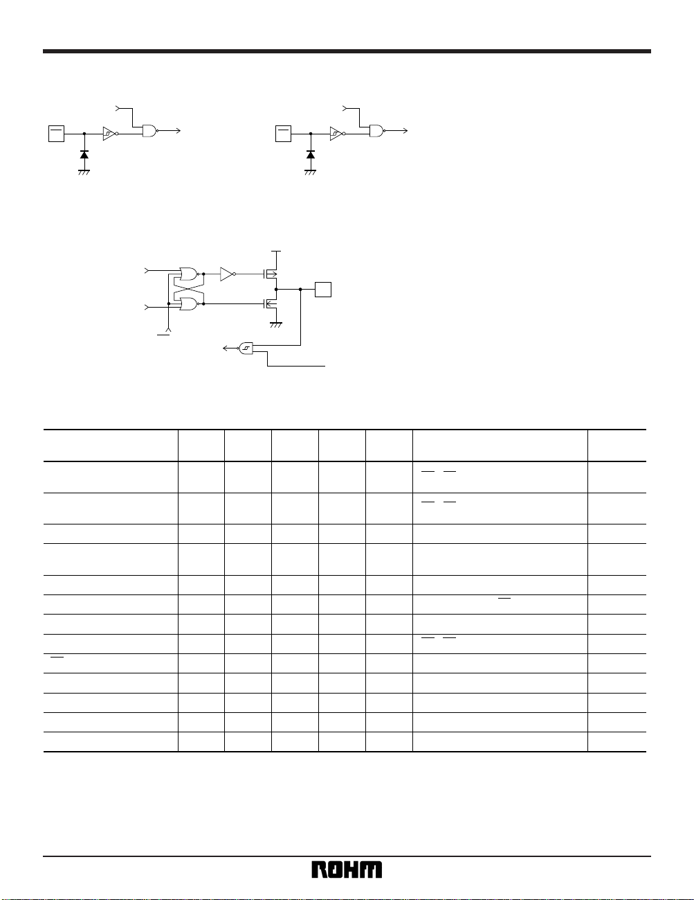
Input circuits
RESET int.
CS
SK
CS int.
•
Output circuits
CS int.
DIO
OE int.
•
Electrical characteristics (unless otherwise noted, Ta = – 20 to + 85°C, VCC = 5V ± 10%)
Input low level voltage
V
IL
Parameter Symbol Min. Typ. Max. Unit
——
0.2 ×
V
CC
V
0.8
×
V
CC
——V
0—0.4 V
VCC –
0.4
—V
CC V
– 1 — 1 µA
–1 — 1 µA
—— 3mA
——200 µA
—— 1 MHz
— 100 — kΩ
— 0.5 1 kΩ
0—VCC V
0—VCC V
Measurement
Circuit
CS, SK, DIO pin
Input high level voltage
V
IH
CS, SK, DIO pin
Output low level voltage
V
OL
IOL = 2.1mA
I
OH = – 0.4mAOutput high level voltage
V
OH
Input leakage current
I
LI
VIN = 0 ~ VCC
Output leakage current
I
LO
VOUT = 0 ~ VCC, CS = VCC
Operating current consumption
ICC
f = 1MHz, tE / W = 10ms (WRITE) Fig.5
Fig.4
Fig.3
Fig.6
Fig.1
—
—
Standby current
I
SB
CS, SK, DIO, VH, VL, VW = VCC Fig.6
SK frequency
f
SK
Total resistance
R
T
If = 10µA
Wiper resistance
R
W
IW = – 1mA Fig.8
Fig.7
—
—
Resistance potential on High side
VVH
—
Resistance potential on Low side
VVL
Conditions
4
Memory ICs BU9831 / BU9831F
(unless otherwise noted, Ta = – 20 to + 85°C, VCC = 3V ± 10%)
Input low level voltage
VIL
Parameter Symbol Min. Typ. Max. Unit
——
0.2 ×
V
CC
V
0.8
×
V
CC
——V
0—0.4 V
VCC –
0.4
—V
CC V
– 1 — 1 µA
– 1 — 1 µA
—— 2mA
——100 µA
——500 kHz
— 100 — kΩ
— 12kΩ
0—VCC V
0—VCC V
Measurement
Circuit
CS, SK, DIO pin
Input high level voltage
VIH
CS, SK, DIO pin
Output low level voltage
VOL
IOL = 100µA
I
OH = – 100µA
Output high level voltage
VOH
Input leakage current
ILI
VIN = 0 ~ VCC
Output leakage current
ILO
VOUT = 0 ~ VCC, CS = VCC
Operating current consumption
ICC
f = 1MHz, tE / W = 10ms (WRITE) Fig.5
Fig.4
Fig.3
Fig.6
Fig.1
—
—
Standby current
I
SB
CS, SK, DIO, VH, VL, VW = VCC Fig.6
SK frequency
f
SK
Fig.7Total resistance
R
T
If = 10µA
Wiper resistance
R
W
IW = – 500µA Fig.8
Resistance potential on High side
VVH
—
Resistance potential on Low side
VVL
—
Conditions
•
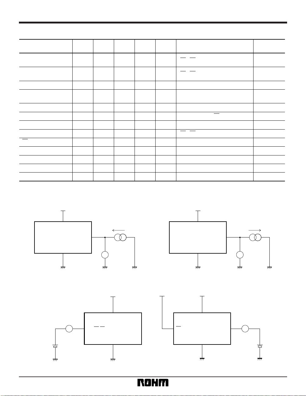
Measurement circuits
VCC
VOL
IOL
VCC
DIO
GND
Data set when output is LOW
V
Fig. 1 LOW output voltage measurement circuit
VCC
VOH
IOH
VCC
DIO
GND
Data set when output is HIGH
V
Fig. 2 HIGH output voltage measurement circuit
VCC
ILI
VCC
DIO, SK, CS
GND
A
VIN = 0 ~ VCC
Fig. 3 Input leakage current measurement circuit
VCCVCC
ILO
VO = 0 ~ VCC
VCC
CS
DIO
GND
A
Fig. 4 Output leakage current measurement circuit
 Loading...