

Page 1

A
High Reliability Serial EEPROMs
WL-CSP EEPROM family
SPI BUS
BU9829GUL-W
●Description
BU9829GUL-W is Serial EEPROM built-in LDO regulator by SPI BUS interface.
●Features
○EEPROM PART
1) 2,048 words×8 bits architecture serial EEPROM
2) Wide operating voltage range (1.6V~3.6V)
3) Serial Peripheral Interface
4) Self-timed write cycle with automatic erase
5) Low Power consumption Write (3.6V) : 1.5mA (Typ.)
Read (3.6V) : 0.5mA (Typ.)
Standby (3.6V) : 0.1µA (Typ.)
6) Auto-increment of registers address for Read mode
7) 32 byte Page Write mode
8) DATA security
Defaults to power up with write-disabled state
Software instructions for write-enable/disable
Block writes protection by status register
Write inhibit at low Vcc
9) Initial data FFh in all address, 00h in status register and 10 in VSET[1:0].
10) Data retention: 10 years
11) Endurance : 100,000 erase/write cycles
○LDO REGULATOR PART
12) Low power consumption
Standby (3.6V) : 0.1 µA (Typ.)
Operation (3.6V) : 0.1mA (Typ.)
13) Power on/off by enable pin
14) Initial LDO output voltage 2.9V
15) Setting output voltage by EEPROM command (VSET WRITE)
●Absolute maximum rating (Ta=25℃)
Parameter Symbol Rating Unit
Supply Voltage
Power Dissipation Pd 220 mW
Storage Temperature Tstg -65 ~ 125 ℃
Operating Temperature Topr -30 ~ 85 ℃
Terminal Voltage - -0.3~Vcc+0.3 V
●EEPROM recommended operating condition
Parameter Symbol Rating Unit
Supply Voltage Vcc1 1.6~3.6
Input Voltage VIN 0~Vcc1
●LDO regulator recommended operating condition
Parameter Symbol Rating Unit
Supply Voltage Vcc2 2.9~3.6
Input Voltage VIN 0~Vcc2
Vcc1(EEPROM)
Vcc2(LDO)
-0.3~4.5 V
No.10001EAT13
V
V
www.rohm.com
© 2010 ROHM Co., Ltd. All rights reserved.
1/16
2010.09 - Rev.
Page 2

BU9829GUL-W
A
Technical Note
●Memory cell characteristics (Ta=25℃, Vcc1=1.6~3.6V) ●Input/output capacity (Ta=25℃, Frequency=5MHz)
Parameter
Write/Erase Cycle *1 100,000 - - Cycle Input Capacitance *1CIN VIN=GND - 8pF
Min. Typ. Max. Min. Max.
Data Retention *1 10 - - Year Output Capacitance*1C
*1 : Not 100% tested *1:Not 100% TESTED
Limits
Unit Parameter Symbol Conditions
OUTVOUT
=GND - 8pF
Limits
Unit
●EEPROM DC operating characteristics (Unless otherwise specified, Ta=-30~85℃, Vcc1=1.6~3.6V)
Parameter Symbol
Min. Typ. Max.
Limits
Unit Test condition
"H" Input Voltage1 VIH1 0.7xVcc1 - Vcc1+0.3 V 2.5≦Vcc1≦3.6V
"H" Input Voltage2 VIH2 0.75xVcc1 - Vcc1+0.3 V 1.6≦Vcc1<2.5V
"L" Input Voltage1 VIL1 -0.3 - 0.3xVcc1 V 2.5V≦Vcc1≦3.6V
"L" Input Voltage2 VIL2 -0.3 - 0.25xVcc1 V 1.6V≦Vcc1<2.5V
"L" Output Voltage1 VOL1 0 - 0.2 V IOL=1.0mA , 2.5V≦Vcc1≦3.6V
"L" Output Voltage2 VOL2 0 - 0.2 V IOL=1.0mA , 1.6V≦Vcc1<2.5V
"H" Output Voltage1 VOH1 Vcc1-0.2 - Vcc1 V IOH=-0.4mA , 2.5V≦Vcc1≦3.6V
"H" Output Voltage1 VOH2 Vcc1-0.2 - Vcc1 V IOH=-100µA , 1.6V≦Vcc1<2.5V
Input Leakage Current ILI -1 - 1 µA VIN=0~Vcc1
Output Leakage Current ILO -1 - 1 µA VOUT=0~Vcc1 , CSB=Vcc1
ICC1 - - 1.5 mA
Operating Current Write
ICC2 - - 2.0 mA
ICC3 - - 0.2 mA
Operating Current Read
ICC4 - - 0.6 mA
Standby Current ISB - - 1.0 µA
○This product is not designed for protection against radioactive rays.
Vcc1=1.8V , fSCK =2MHz, tE/W=5ms
Byte Write, Page Write, Write Status Register
Vcc1=2.5V , fSCK =5MHz,tE/W=5ms
Byte Write, Page Write, Write Status Register
Vcc1=1.8V , fSCK=2MHz , SO=OPEN
Read, Read Status Register
Vcc1=2.5V , fSCK=5MHz,SO=OPEN
Read, Read Status Register
Vcc1=3.6V , CSB=Vcc1 , SCK ,
SI=Vcc1/GND ,SO=OPEN
●EEPROM AC operating characteristics (Ta=-30~85℃)
Parameter Symbol
1.6≦VCC1<1.8V 1.8≦VCC1≦3.6V
Min. Typ. Max. Min. Typ. Max.
Unit
SCK clock Frequency fSCK - - 2.5 - - 5 MHz
SCK High Time tSCKWH 200 - - 80 - - ns
SCK Low Time tSCKWL 200 - - 80 - - ns
CSB High Time tCS 200 - - 90 - - ns
CSB Setup Time tCSS 150 - - 60 - - ns
CSB Hold Time tCSH 150 - - 60 - - ns
SCK Setup Time tSCKS 50 - - 50 - - ns
SCK Hold Time tSCKH 50 - - 50 - - ns
SI Setup Time tDIS 50 - - 20 - - ns
SI Hold Time tDIH 50 - - 20 - - ns
Output Data Delay Time tPD - - 100 - - 80 ns
Output Hold Time tOH 0 - - 0 - - ns
Outuput Disable Time
SCK Rise Time
SCK Fall Time
Output Rise Time
Output Fall Time
*1
tOZ - - 200 - - 80 ns
*1
tRC - - 1 - - 1 µs
*1
tFC - - 1 - - 1 µs
*1
tRO - - 50 - - 50 ns
*1
tFO - - 50 - - 50 ns
Write Cycle Time tE/W - - 5 - - 5 ms
Wait Time From Vcc1 ON To
EEPROM Command
*1 : Not 100% tested
tON 15 - - 15 - - ms
www.rohm.com
© 2010 ROHM Co., Ltd. All rights reserved.
2/16
2010.09 - Rev.
Page 3

BU9829GUL-W
A
Technical Note
●Synchronous data input/output timing
VCC1
CSB
SCK
SI
SO
tON
tSCKS
tCSS
tSCKWL tSCKWH
tDIH
tDIS
Hi-Z
tRC
CSB
SCK
tFC
SI
SO
tPD
tOH
tCSH
tRO,tFO
tCS
tSCKH
tOZ
Hi-Z
Fig.1 Input timing
Fig.2 Input and output timing
SI data is latched into the chip at the rising edge of SCK clock.
Address and data must be transferred from MSB.
SO data toggles at the falling edge of SCK clock.
Output data toggles from MSB.
●AC condition
Parameter Symbol
Limits
Min. Typ. Max.
Unit
Load Capacitance CL - - 100 pF
Input Rise times - - - 50 ns
Input Fall times - - - 50 ns
Input Pulse Voltage - 0.25Vcc1/0.75Vcc1 V
Input and Output Timing Reference Voltages - 0.3VCc1/0.7Vcc1 V
●Pin configuration ●Pin function
Land
No.
C
C1
B
B1
A
A1
C2
B2
A2
C3
B3
A3
INDEX POST
A1 Vcc1 - Power Supply (EEPROM)
A2 CSB IN Chip Select Control
A3 SCK IN Serial Data Clock Input
B1 Vcc2 - Power Supply (LDO)
B2 SI IN Start Bit, Op.code, Address, Serial Data Input
Pin
Name
I/O Function
B3 SO OUT Serial Data Output
1
2
3
C1 V
OUT LDO Regulator Output
OUT
C2 GND - Ground (0V)
Fig.3 Pin configuration (bottom view)
C3 LDOEN IN LDO Regulator Enable
●LDO regulator DC operating characteristics (Unless otherwise specified Ta=-30~85℃)
Parameter Symbol
Specification
Min. Typ. Max.
Unit test condition
Output Voltage1-1 VOUT1-1 2.9 3.0 3.2 V 3.2V≦Vcc2≦3.6V, IOUT=0, 2mA, VSET=1, 0=[1:1]
Output Voltage1-2 VOUT1-2 2.9 3.0 3.1 V 3.2V≦Vcc2≦3.6V, IOUT=2, 10mA, VSET=1, 0=[1:1]
Output Voltage2-1 VOUT2-1 2.8 2.9 3.1 V 3.1V≦Vcc2≦3.6V, IOUT=0, 2mA, VSET=1, 0=[1:0]
Output Voltage2-2 VOUT2-2 2.8 2.9 3.0 V 3.1V≦Vcc2≦3.6V, IOUT=2, 10mA, VSET=1, 0=[1:0]
Output Voltage3-1 VOUT3-1 2.7 2.8 3.0 V 3.0V≦Vcc2≦3.6V, IOUT=0, 2mA, VSET=1, 0=[0:1]
Output Voltage3-2 VOUT3-2 2.7 2.8 2.9 V 3.0V≦Vcc2≦3.6V, IOUT=2, 10mA, VSET=1, 0=[0:1]
Output Voltage4-1 VOUT4-1 2.6 2.7 2.9 V 2.9V≦Vcc2≦3.6V, IOUT=0, 2mA, VSET=1, 0=[0:0]
Output Voltage4-2 VOUT4-2 2.6 2.7 2.8 V 2.9V≦Vcc2≦3.6V, IOUT=2, 10mA, VSET=1, 0=[0:0]
Operating Current ICC - - 200 µA Vcc2=3.6V, IOUT=0A
Standby Current ISB - - 1.0 µA Vcc2=3.6V, IOUT=0A, LDOEN=GND
“H” Input Voltage VIH 1.4 - Vcc2+0.3 V 2.9V≦Vcc2≦3.6V
“L” Input Voltage VIL -0.3 - 0.6 V 2.9V≦Vcc2≦3.6V
○This product is not designed for protection against radioactive rays.
www.rohm.com
© 2010 ROHM Co., Ltd. All rights reserved.
3/16
2010.09 - Rev.
Page 4
BU9829GUL-W
A
r
y
Technical Note
●LDO regulator AC operating characteristics
Parameter Symbol
Specification
Min. Typ. Max.
Unit Test condition
Vcc1 Rise Time tVCC1 - - 5 msec VCC1 x 0%→VCC1 x 95% point
LDOEN Wait Time tLDOEN 15 - - msec VCC1 x 0%point→ LDOEN=High
●Output voltage depend on VSET bit
The 2bit data are stored into the VSET memory and output voltage change among VOUT1~VOUT4.
VSET data are Written into non-volatile memory array. Initial VSET data is 1,0 in VSET[1:0] and VOUT is 2.9V.
STEP VOUT(typ.) [V] VSET1 VSET0
VOUT1
VOUT2
VOUT3
VOUT4
3.0
2.9
2.8
2.7
1
1
0
0
1
0
1
0
●Input power supply regulation timing
①Using EEPROM PART
In case of using EEPROM part, be sure to raise Vcc1 up to operating voltage. In this time, Vcc2 has no connection with
operating.
Vcc1
EEPROM
EEPROM部電源
Power Supply
Vcc2
LDOレギュレータ部電源
LDO regulator
Power Supply
Not
動作不可 EEPROM動作可能範囲 動作不可 EEPROM動作可能範囲 動作不可
Operating
Operating
Not
Operating
Operating
Not
Operating
Fig.4 Using EEPROM Part, Regulation Timing
②Using LDO regulator part
In case of using LDO regulator part, be sure to raise Vcc1 and Vcc2 up to operating voltage.
After rising Vcc1, wait 15msec and rising LDOEN.
When LDOEN is raised, Vcc1 must be operating voltage.
tVcc1:MAX 5msec
tVcc1:MAX 5msec
Vcc1
EEPROM
Power Suppl
Vcc2
LDO regulato
Power Supply
LDOEN
t
LDOEN : MIN 15msec
t
LDOEN : MIN 15msec
Not
Operating
Operating
Not
Operating
Operating
Not
Operating
Fig.5 Using LDO Regulator Part, Regulation Timing
www.rohm.com
© 2010 ROHM Co., Ltd. All rights reserved.
4/16
2010.09 - Rev.
Page 5

BU9829GUL-W
A
●Block diagram
CSB
SCK
INSTRUCTION
DECODE
CONTROL CLOCK
GENERATION
SI
INSTRUCTION
REGISTER
ADDRESS
REGISTER
INHIBITION
DETECTION
WRITE
11bit
VOLTAGE
ADDRESS
DECODER
SO
DATA
REGISTER
8bit
VOUT
AMP
+
B.R
RESISTOR
Fig.6 Block diagram
●Characteristic data (The following characteristic data are typical values.)
5
Ta=-30℃
4
Ta=25℃
Ta=85℃
3
VIH[V]
2
1
0
01234
Fig.7 "H" input voltage VIH (EEPROM)
3
2.5
2
1.5
VOH[V]
1
0.5
0
0 0.4 0.8 1.2
4
3
SPEC
Vcc[V]
SPEC
Ta=-30℃
Ta=25℃
Ta=85℃
IOH[mA]
Fig.10 "H" output voltage VOH
fSCK=2MHz
DATA=00h
SPEC
2
ICC1[mA]]
1
0
01234
Fig.13 Current consumption at WRITE operation ICC1
www.rohm.com
SPEC
© 2010 ROHM Co., Ltd. All rights reserved.
Vcc[V]
Ta=-40℃
Ta=-30℃
Ta=25℃
Ta=85℃
5
Ta=-30℃
4
Ta=25℃
Ta=85℃
3
VIL[V]
2
1
0
01234
Fig.8 "L" input voltage VIL (EEPROM)
5
4
Ta=-30℃
Ta=25℃
3
Ta=85℃
ILI[μA]
2
1
0
01234
Fig.11 Input leak current ILI
2.5
fSCK=2MHz
2
DATA=AAh
1.5
1
ICC3(READ)[mA]
0.5
0
01234
Fig.14 Consumption Current at READ operation ICC3
SPEC
Vcc[V]
Vcc[V]
Vcc[V]
SPEC
Ta=-30℃
Ta=25℃
Ta=85℃
5/16
HIGH VOLTAGE
GENERATOR
11bit
16,384 bit
EEPROM
R/W
8bit
AMP
LDOEN
2bit
VOUT SETTING REGISTER
1
Ta=-30℃
Ta=25℃
0.8
Ta=85℃
0.6
VOL[V]
0.4
0.2
SPEC
0
0123
5
4
Ta=-30℃
Ta=25℃
3
Ta=85℃
ILO[μA]
2
1
0
01234
Fig.12 Output leak current ILO
12
10
Ta=-30℃
Ta=25℃
Ta=85℃
8
6
ISB[μA]
4
2
0
01234
Fig.15 Standby operation ISB (EEPROM)
Technical Note
SPEC
IOL[mA]
Fig.9 "L" output voltage VOL
SPEC
VOUT[V]
SPEC
Vcc[V]
2010.09 - Rev.
Page 6

BU9829GUL-W
A
(
)
●Characteristic data
100
10
fSCK[MHz]
1
Ta=-30℃
Ta=25℃
Ta=85℃
0.1
01234
250
200
Ta=-30℃
Ta=25℃
150
Ta=85℃
tCS[ns]
100
50
0
01234
60
40
Ta=-30℃
Ta=25℃
Ta=85℃
tDIS[ns]
20
SPEC
Vcc[V]
Fig.16 SCK frequency fSCK
SPEC
Vcc[V]
Fig.19 CSB high time tCS
SPEC
SPEC
SPEC
SPEC
www.rohm.com
© 2010 ROHM Co., Ltd. All rights reserved.
0
01234
250
200
Ta=-30℃
Ta=25℃
150
Ta=85℃
tOZ [ns]
100
50
0
01234
3
2.5
Ta=-30℃
Ta=25℃
Ta=85℃
2
1.5
VIH[V]
1
0.5
0
01234
Fig.28 "H" input voltage VIH (L DO)
3.2
3.1
3
VOUT[V]
2.9
2.8
2.7
0246810121416
Vcc[V]
Fig.22 SI setup time tDIS
SPEC
Fig.25 Output disable time tOZ
SPEC
Vcc[V]
Vcc[V]
Ta=-30℃
Ta=25℃
Ta=85℃
SPEC
SPEC
Iout[mA]
Fig.31 Vout response (LDO)
VSET=1,0
SPEC
SPEC
250
200
150
100
tSCKWH [ns]
50
0
01234
200
160
120
tCSS[ns]
80
40
0
01234
60
40
tDIH[ns]
20
0
01234
8
6
4
tE/W[ms]
2
0
01234
3
2.5
2
1.5
VIL[V]
1
0.5
0
250
200
150
ICC[uA]
100
50
SPEC
Ta=-30℃
Ta=25℃
Ta=85℃
Vcc[V]
Fig.17 SCK high time tSCKWH
SPEC
Ta=-30℃
Ta=25℃
Ta=85℃
Vcc[V]
Fig.20 CSB setup time tCSS
SPEC
Ta=-30℃
Ta=25℃
Ta=85℃
Vcc[V]
Fig.23 SI hold time tDIH
SPEC
Ta=-30℃
Ta=25℃
Ta=85℃
Vcc[V]
Fig.26 Write cycl e time tE/W
Ta=-30℃
Ta=25℃
Ta=85℃
01234
Fig.29 "L" input voltage VIL (LDO)
Ta=-30℃
Ta=25℃
Ta=85℃
0
01234
Fig.32 Current consumption ICC (LDO)
Vcc[V]
Vcc[V]
SPEC
SPEC
SPEC
SPEC
SPEC
6/16
Technical Note
250
200
Ta=-30℃
150
Ta=25℃
Ta=85℃
100
tSCKWL [ns]
50
0
01234
200
160
Ta=-30℃
120
Ta=25℃
Ta=85℃
tCSH[ns]
80
40
0
01234
120
100
80
60
tPD [ns]
40
20
0
01234
8
6
Ta=-30℃
4
Ta=25℃
ISB[us]
Ta=85℃
2
0
01234
Fig.27 Standby operation ISB (LDO)
160
120
Ta=-30℃
Ta=25℃
Ta=85℃
80
tVcc1[us]
40
0
01234
SPEC
SPEC
Vcc[V]
Fig.18 SCK low time tSCKWL
SPEC
SPEC
Vcc[V]
Fig.21 CSB hold time tCSH
SPEC
SPEC
Ta=-30℃
Ta=25℃
Ta=85℃
Vcc[V]
Fig.24 Data output delay time tPD
Vcc[V]
=
Vcc[V]
Fig.30 Vcc1 rise time tVcc1
2010.09 - Rev.
SPEC
Page 7

BU9829GUL-W
A
Technical Note
●Functional description
○Status Register
The device has status register.
Status register consists of 8bits and is shown following parameters.
2 bits (BP0 and BP1) are set by “Write Status Register” commands, which are non-volatile.
Specification of endurance and data retention are as well as memory array. WEN bit is set by “Write Enable” and “Write
Disable” commands. After power become on, the device is disable mode.
B/R bit is a read-only and status bit.
The device is clocked out value of the status register by “Read Status Register” command input.
Bit7 Bit6 Bit5 Bit4 Bit3 Bit2 Bit1 Bit0
0 0 0 0 BP1 BP0 WEN
B/R
Bit Definition
BP0/BP1
Block write protection for memory array
(EEPROM)
Write enable/disable status bit
WEN
WEN=0 : write disable
WEN=1 : write enable
BP1 BP0 Block Write Protection
0
0
1
1
0
1
0
1
NONE
600h-7FFh
400h-7FFh
000h-7FFh
READY/BUSY status bit
B/R
B/R
=0 : READY
B/R
=1 : BUSY
●Instruction code
Instruction Operation Op.Code Address
WREN Write enable 0000 0110 -
WRDI Write disable 0000 0100 READ Read data from memory array 0000 0011 A10 ~ A0
WRITE Write data to memory array 0000 0010 A10 ~ A0
RDSR Read status register 0000 0101 WRSR Write status register 0000 0001 -
VSET_READ Read VSET data 0000 0011 800h
VSET_WRITE Write VSET data 0000 0010 800h
●Timing chart
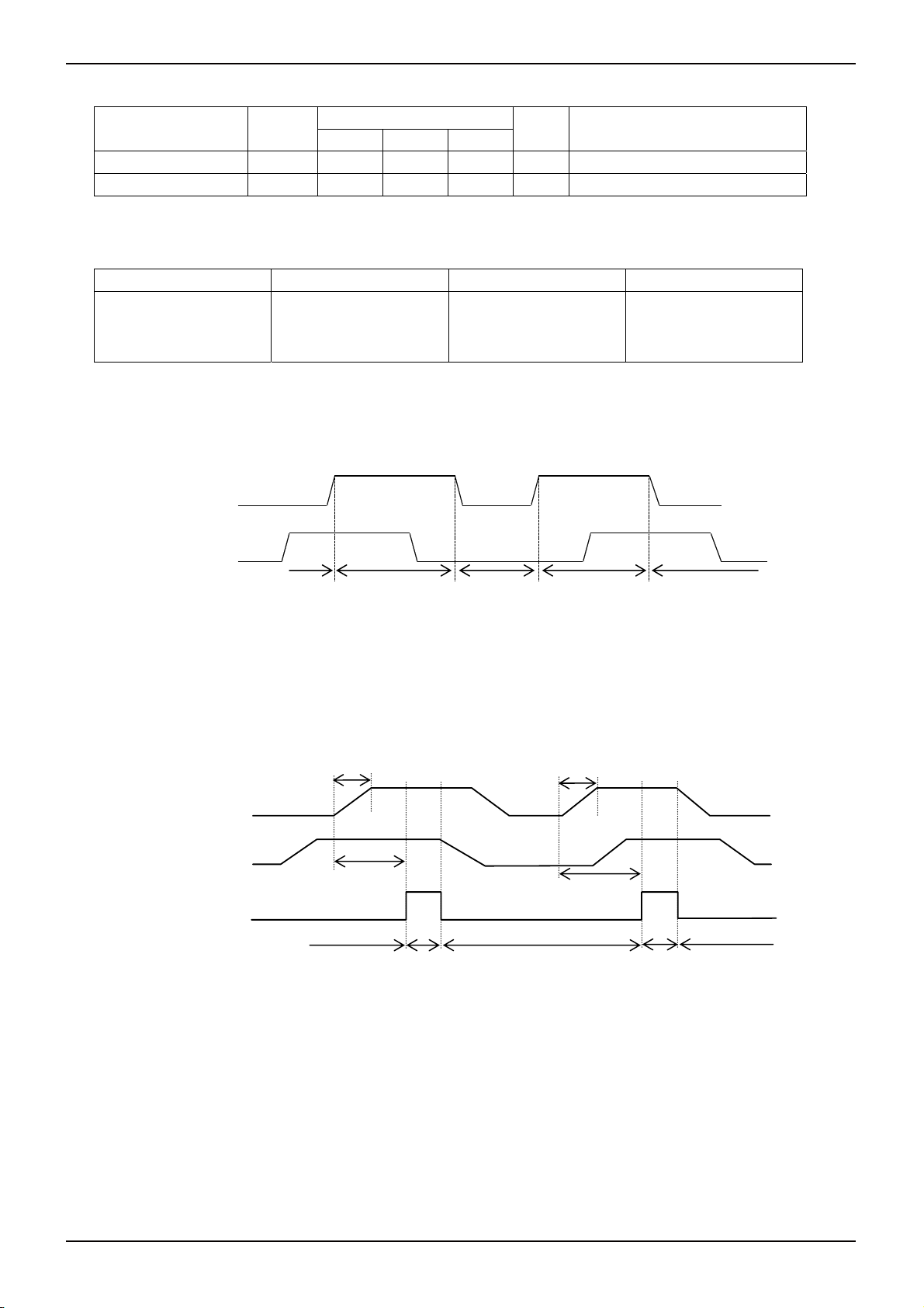
1. WRITE ENABLE 2. WRITE DISABLE
CSB
CSB
5
SCK
12 45
7603
SCK
60312 4 7
SI
00001010
SI
0
00
00100
SO
Hi-Z
SO
Hi-Z
Fig.33 WRITE ENABLE CYCLE TIMING
Fig.34 WRITE DISABLE CYCLE TIMING
○The device has both of the enable and disable mode. After “Write Enable” is executed, the device becomes in the enable
mode. After “Write Disable” is executed, the device becomes in the disable mode. After CSB goes low, each of Op.code
is recognized at the rising edge of 7th clock. Each of instructions is effective inputting seven or more SCK clocks. This
“Write Enable” instruction must be proceeded before the any write commands. The device ignores inputting the any write
commands in the disable mode. Once the any write commands is executed in the enable mode, the device becomes the
disable mode. After the power become on, the device is in the disable mode.
www.rohm.com
© 2010 ROHM Co., Ltd. All rights reserved.
7/16
2010.09 - Rev.
Page 8

BU9829GUL-W
A
A0A
2
~
A0A
2
5
0
Technical Note
3. READ
The data stored in the memory are clocked out after “Read” instruction is received. After CSB goes low, the address need
to be sent following by Op.code of “Read”. The data at the address specified are clocked out from D7 to D0, which is start
at the falling edge of 23th clock. This device has the auto-increment feature that provides the whole data of the memory
array with one read command, outputs the next address data following the addressed 8bits of data by keeping SCK
clocking. When the highest address is reached, the address counter rolls over to the lowest address allowing the
continuous read cycle.
CSB
SCK
SO
SI
0 3 71 2
0 0 0 0 0
Hi - Z
~
~ ~
**
~ ~
~ ~
~
~
0A10
4 5
6 8
11
0
Fig.35 READ CYCLE TIMING
~ ~
~ ~
14
~ ~
~ ~
~
~
23 30 24
1
D7
D6
~ ~
~ ~
~ ~
~
~
D
~
~
D1
*=Don't care
D0
4. WRITE
This “Write” command writes 8bits of data into the specified address. After CSB goes low, the address need to be sent
following by Op.code of “Write”. Between the rising edge of the 29th clock and it of the 30th clock, the rising edge of CSB
initiates high voltage cycle, which writes the data into non-volatile memory array, but the command is cancelled if CSB is
high except that period. It takes maximum 5ms in high voltage cycle (tE/W). The device does not receive any command
except for “Read Status Register” command during this high voltage cycle. This device is capable of writing the data of
maximum 32byte into memory array at the same time, which keep inputting two or more byte data with CSB “L” after
8bits of data input. For this Page Write commands, the eight higher order bits of address are set, the six low order
address bits are internally incremented by 5bits of data input. If more than 16 words, are transmitted the address counter
“roll over”, and the previous transmitted data is overwritten.
CSB
SCK
SI
1
0 3 7 8
4
1
0
~
~
~
~
~
~
~
~
0A1
~
~
14
~
~
~
~
~
~
23 30
1
~
~
~
~
24
31
~
~
D60
~
~
D0 0 0 0 0 0 D2 D1 D7
SO
Hi-Z
Fig. 36 WRITE CYCLE TIMING
~
~
~ ~
~ ~
*=Don't care
5. RDSR (READ STATUS REGISTER)
The data stored in the status register is clocked out after “Read Status Register” instruction is received.
After CSB goes low, Op.colde of “Read Status Register” need to sent. The data stored in the status register is clocked out
of the device on the falling edge of 7th clock. Bit7, Bit6, Bit5 and Bit4 in the status register are read as 0.
This device has the auto-increment feature as well as “Read” that output the 8bits of the same data following it to keep
SCK clocking. It is possible to see ready and busy state by executing this command during tE/W. If more than 16 words,
are transmitted the address counter “roll over” and the previous transmitted data is overwritten.
CSB
SCK
1 2
0
3
4
7
6
5
9
8
11
10
13
12
15
14
SI
1
0
0
0
0 0
0
1
Bit6
Bit5
00
SO
Hi-Z
Bit7
0
Bit4
Bit3
BP1
BP00
Bit2
Bit1
WEN
Bit0
R/B
Fig.37 READ STATUS REGISTER CYCLE TIMING
www.rohm.com
© 2010 ROHM Co., Ltd. All rights reserved.
8/16
2010.09 - Rev.
Page 9

BU9829GUL-W
A
Technical Note
6. WRSR (WRITE STATUS RESISTER)
This “Write Status Register” command writes the data, two (BP1, BP0) of the eight bits, into the status register. Write
protection is set by BP1 and BP0 bits. After CSB goes low, Op.code of “Read Status Register” need to sent. Between the
rising edge of the 15th clock and it or the 16th clock, the rising edge of CSB initiates high voltage cycle, which writes the
data into non-volatile memory array, but the command is cancelled if CSB is high except that period. It takes maximum
5ms in high voltage cycle (tE/W) as well as “Write”.Block write protection is determined by BP1 and BP0 bits, which is
selected from quarter, half and the entire memory array. (See Table2 BLOCK WRITE PROTECTION>)
CSB
SCK
SI
1 2
0
0
0 0 0 0
3
4
6
5
1
1
0
7
9
8
Bit7 Bit6
* * * * BP1
10
Bit5 Bit4 Bit3
15
11
12
Bit2 Bit1 Bit0
BP0
14
13
*
*
Hi-Z * Don’t care
SO
Fig. 38 WRITE STATUS REGISTER WRITE CYCLE TIMING
7. VSET READ
The VSET data stored in the memory are clocked out after “VSET Read” instruction set address 800h is received.
After CSB goes low, the address (800h) need to be sent following by Op.code of “Read”. 0 are clocked out from D7 to D2
and the VSET data are clocked out from D1 to D0, which is start at the falling edge of 23th clock.
CSB
SCK
7
6
5
2
1
0
3
4
8
13
12
24
23
30
SI
SO
Hi-Z
0
0
0
0 0
1
0
Fig.39 VSET READ CYCLE TIMIING
* * 1 0
1
0 0
0 0 0 0
VSET 1 VSET
* Don’t care
0
8. VSET WRITE
This “Write” command set address 800h writes VSET data into VSET1 and VSET0 memory array. After CSB goes low,
the address (800h) and VSET data need to be sent following by Op.code of “VSET Write”. Between the rising edge of the
29th clock and it of the 30th clock, the rising edge of CSB initates high voltage cycle, which writes the data into
non-volatile memory array, but the command is cancelled if CSB is high except that period. It takes maximum 5ms in high
voltage cycle (tE/W). The device does not receive any command except for “Read Status Register” command during this
high voltage cycle.
CSB
SCK
1
0
3
2
5
4
7
6
8
13
12
24
23
30
31
SO
SI
0 0 0 0 0
Hi-Z
0
1
0
* * 1
0 0 0 0
* *
*
Fig. 40 VSET WRITE CYCLE TIMING
*
VSET 1 VSET
0
* Don’t care
www.rohm.com
© 2010 ROHM Co., Ltd. All rights reserved.
9/16
2010.09 - Rev.
Page 10

BU9829GUL-W
A
Technical Note
●EEPROM soft ware
○READ, VSET_READ, RDSR Command cancel
Cancel of these commands is possible by changing CSB pin to “HIGH” in all sections.
OPECODE ADDRESS DATA
8bit 8bit
Cancel is possible
8bit
Fig.41 READ, VSET_READ Cancel Timing
OPECODE DATA
8bit 8bit
Cancel is possible
Fig.42 RDSR Cancel Timing
○WRITE, PAGE_WRITE, VSET_WRITE、WRSR Command cancel
Cancel of these write command is possible by changing CSB pin to “HIGH” in opecode, address and data input sections
(section a~b), but it is impossible after data input section (section c~d), if Vcc1 is OFF during tE/W, please write again
because write data is not guaranteed in specified address, if SCK and CSB rise at the same time in section C, command
is instability. It is recommend to rise CSB in “SCK=L” section.
OPECODE
8bit
ADDRESS DATA(n) tE/W
8bit 8bit
a
b d
c
AN ENLARGEMENT
Fig.43 WRITE, PAGE_WRITE, VSET_WRITE READ VSET_READ Cancel Timing
SCK
D7 bD6 D5 D4 D3 D2 D1 D0
SI
c
OPECODE
8bit
a
DATA(n) tE/W
8bit 8bit
b d
c
Fig.44 WRSR Cancel Timing
AN ENLARGEMENT
SCK
SI
14
D1 D0
b
15
16
17
c
d
○WREN, WRDI command cancel
Cancel of these commands is possible by changing CSB pin to “HIGH” of opecode to rising 8 clk, but it is impossible after
rising 8 clk. In the case, please send WREN or WRDI cancel timing command again.
OPECODE
8bit
a
b
AN ENLARGEMENT
78
a
9
b
Fig.45 WREN, WRDI Cancel Timing
●Data polling
If RDSR command is carried out daring tE/W, according to out put data (
B/R bit), to monitor READY/BUSY state is
possible. Because of this, it is possible to send next command earlier than regular programming time (tE/W MAX=5ms).
B/R
If
bit is “1”, EEPROM’s state is “BUSY”. If this becomes “0”, it is possible to send next command to change
EEPROM to “READY” state. Status register data read by this command in tE/W is not data written by WRSR command but
old data before. Status register data in each section is shown below.
CSB
During WRSR Command(tE/W)
BUSY
READY
SCK
SI
SO
READ STATUS
REGISTOR
a=0Ch b=(00h) c=0Fh
WRITE STATUS
REGISTOR
READ STATUS
REGISTOR
READ STATUS
REGISTOR
d=0Ch
READ STATUS
REGISTOR
e=00h
Fig.46 Status register data in each section
www.rohm.com
© 2010 ROHM Co., Ltd. All rights reserved.
10/16
2010.09 - Rev.
Page 11

BU9829GUL-W
A
Technical Note
●EEPROM part
1. Hardware Connection of EEPROM
EEPROM may have malfunction owing to noise signal for input pin, and movement in the low voltage region at power
ON/OFF. These malfunctions may occur, especially at min voltage limit of EEPROM or below.
To avoid this, please note about hardware connection showed as follows.
1.1 Input Terminals
Input equivalent circuits of CSB, SCK and SI are showed Fig.47, 48.
Input terminal is connected between CMOS schmitt trigger input circuit and input protection circuit.
These pin are not pull up or pull down, therefore please don’t input Hi-Z in use. And please make CSB “HIGH” in the
low voltage region at power ON/OFF. If CSB is "LOW" at power ON/OFF, malfunction may occur. To make other input
terminals pull up or pull down is recommendable.
CSB
SCK, SI
Fig.47 CSB terminals
equivalent circuit
Fig.48 SCK,SI terminals
equivalent circuit
Fig.49 SO terminals
equivalent circuit
1.2 Output Terminals
Output equivalent circuit of so is showed Fig.49. This output terminal is 3 states buffer.
The data is output from so at output timing by READ command, so is Hi-z except this timing. If EEPROM malfunction
occur by Hi-z input of the microcontroller port connected with so, please make so pull up or pull down. If it doesn’t
affected the microcontroller movement to make so open, it is no problem. Load capacity of so disturb high speed
movement of EEPROM. If this load capacity is 100pF or below, BU9829GUL-W can move in 2.5MHz
(Vcc1=1.6V~1.8V) or 5MHz (Vcc1=1.8V~3.6V)
1.3 Input pin pull up, pull down resistance
The design method of pull up/pull down resistance for input and output are as follows.
1.3.1 Pull up resistance Rpu of input terminals
Microcontroller EEPROM
V
OLM
I
OLM
Rpu
V
ILE
“L” output
“L” input
Rpu ≧
VOLM ≦ VILE
Example) When Vcc=5V, VILE=1.5V, VOLM=0.4V, IOLM=2mA,
VCC-V
I
OLM
OLM
from the equation①,
…①
…②
Fig.50 Input terminal pull up resistance
Rpu ≧
∴Rpu
5-0.4
-3
2×10
≧ 2.3[kΩ]
・V
ILE : EEPROM VIL specifications
OLM : Microcontroller VOL specifications
・V
・I
OLM : Microcontroller IOL specifications
With the value of Rpu to satisfy the above equation, VOLM
becomes 0.4V or below, and with V
ILE(=1.5V), the equation
② is also satisfied.
SO
www.rohm.com
© 2010 ROHM Co., Ltd. All rights reserved.
11/16
2010.09 - Rev.
Page 12

BU9829GUL-W
A
1.3.2 Pull down resistance Rpd of input terminals
Rpd
EEPROM
“H” input
Microcontroller
V
“H” output
OHM
I
OHM
Fig.51 Input terminals Pull down resistance
・VIHE : EEPROM VIH specifications
OHM : Microcontroller VOH specifications
・V
・IOHM : Microcontroller IOH specifications
1.3.3 Pull up resistance Rpu of SO pin
Microcontroller EEPROM
V
ILM
Rpu
I
OLE
“L” input
Fig.52 SO Pull up resistance
“L” output
・V
OLE : EEPROM VOL specifications
OLE : Microcontroller IOL specifications
・I
・V
ILM : Microcontroller VIL specifications
1.3.4 Pull up resistance Rpu of SO pin
EEPROM
Microcontroller
V
IHM
V
OHE
“H” input
Rpd
I
OHE
“H” output
Fig.53 SO Pull down resistance
・V
OHE : EEPROM VOH specifications
OHE : EEPROM IOH specifications
・I
・V
IHM : Microcontroller VIH specifications
Technical Note
V
Rpd ≧
V
≦ V
V
IHE
OHM
OHM
I
OHM
IHE
Example) When Vcc=5V, V
from the equation①,
Rpd ≧
∴Rpd
≧ 1.2 [kΩ]
2.4
2×10
-3
With the value of Rpd to satisfy the above equation, V
becomes 2.4V or higher, and with V
also satisfied.
VCC-V
Rpu ≧
V
≦ V
V
OLE
OLE
I
ILM
OLE
OLE
Example) When Vcc=5V, VOLE=0.4V, VILM=1.5V, IOLE=2.1mA,
from the equation①,
Rpu ≧
∴Rpu
≧ 2.2 [kΩ]
5-0.4
2.1×10
-3
With the value of Rpd to satisfy the above equation, VOLE
becomes 0.4V or higher, and with V
also satisfied.
V
Rpd ≧
V
≧ V
OHE
I
OHE
IHM
OHE
Example) When Vcc=5V, VOHE=Vcc-0.5V, VIHM=Vccx0.7V, IOHE=0.4mA,
from the equation①,
Rpd ≧
∴Rpd
≧ 11.3 [kΩ]
5-0.5
0.4×10
-3
With the value of Rpu to satisfy the above equation, VOHE
becomes 4.5V or higher, and with V
also satisfied.
…①
…②
IHE=3.5V, VOHM=2.4V, IOHM=2mA,
OHM
IHE(=3.5V), the equation②is
…①
…②
ILM(=1.5V), the equation②is
…①
…②
IHM(=3.5V), the equation ② is
www.rohm.com
© 2010 ROHM Co., Ltd. All rights reserved.
12/16
2010.09 - Rev.
Page 13

BU9829GUL-W
A
Technical Note
●LDO regulator part
LDO regulator part of BU9829GUL-W is CMOSLDO of low power consumption. The data are stored into EEPROM and
output voltage change among 2.7~3.0V. 1step is 0.1V. LDO regulator part had LDOEN pin and VOUT pin. To make this
LDOEN pin LOW is standby mode of low power consumption.
○LDOEN Input Terminals
Input equivalent circuit of LDOEN is showed Fig.54. Input terminal is connected between input circuits made from NMOS
and pull up and input protection circuit. This pin is not pull up or pull down, therefore please don’t input Hi-z. If LDOEN is
LOW, all circuit don’t move and LDO part is standby mode of low power consumption.
LDOEN
VREF
Fig.54 VOUT output terminals
Fig.55 VOUT output terminals
-
+
VOUT
○VOUT Output Terminals
Output equivalent circuit of VOUT is showed Fig.55. If LDOEN is HIGH, LDO regulator output regulate voltage from
VOUT pin. If LDOEN is LOW, VOUT pin is GND by VOUT-GND resistance. Output overshoots change by output capacity,
in actual use, please evaluate and decide output capacity.
VOUT
172mV
Oscilloscope Tektronix TDS3034B
Power source SHOWA 317B
13.6us
rising 1us
IOUT=0→4mA
VCC=3.0V
VCC
VOUT
LDO_EN
0.1uF
Input pulse
measurement circuit
700Ω
Rohm
K2095N
current
probe
VOUT
88mV
20us
Oscilloscope Tektronix TDS3034B
Power source SHOWA 317B
rising 1us
IOUT=0→4mA
VCC=3.0V
VCC
VOUT
LDO_EN
0.1uF
Input pulse
measurement circuit
BU9829GUL-W Evaluation result
(I
=0mA→4mA,C
OUT
=1.0uF)
OUT
Fig.56 CL=0µF Transitional response
BU9829GUL-W Evaluation result
=0mA→4mA,C
(I
OUT
OUT
=0.1uF)
Fig.57 CL=0.1µF Transitional response
VOUT
40mV
Oscilloscope Tektronix TDS3034B
Power source SHOWA 317B
12us
rising1us
IOUT=0→4mA
VCC=3.0V
VCC
measurement circuit
LDO_EN
VOUT
Input pulse
0.1uF
current
probe
700Ω
Rohm
K2095N
VOUT
40mV
120us
Oscilloscope Tektronix TDS3034B
Power source SHOWA 317B
rising 1us
IOUT=0→4mA
VCC=3.0V
VCC
VOUT
LDO_EN
0.1uF
Input pulse
measurement circuit
BU9829GUL-W Evaluation result
(I
=0mA→4mA,C
OUT
OUT
=1.0uF)
Fig.58 CL=1.0µF Transitional response
BU9829GUL-W Evaluation result
(I
=0mA→4mA,C
OUT
=1.0uF)
OUT
Fig.59 CL=10µF Transitional response
700Ω
Rohm
K2095N
700Ω
Rohm
K2095N
current
probe
current
probe
www.rohm.com
© 2010 ROHM Co., Ltd. All rights reserved.
13/16
2010.09 - Rev.
Page 14

BU9829GUL-W
A
Technical Note
○Package power dissipation
Package power dissipation of BU9829GUL-W is 220mW. It is the value at environmental temperature is 25℃. In the case
of use at 25℃ or higher, degradation is done at 2.2W/℃. If output current is very large, please take care of package
power dissipation.
300
200
Pd [mW]
100
許容損失(Pd) [mW]
0
-50 -25 0 25 50 75 100 125 150
Ta [℃]
周囲温度(Ta) [℃]
Fig.60 Package power dissipation
○Large Current Protection Circuit
VOUT terminal has large current protection circuit. This circuit protects IC from large current. However, this protection
circuit effective unexpected accident. Please avoid continual use of protection circuit.
3
2.5
2
1.5
1
0.5
VOUT output v oltage[V]
0
0 5 10 15 20
VOUT load current [mA]
Fig.61 Large Current Protection Circuit
●POR circuit
This IC has a POR (Power On Reset) circuit as mistake write countermeasure. After POR action, it gets in write disable.
The POR circuit is valid only when power is ON, and does not work when power is OFF. When power is ON, if the
recommended conditions of the following tR, tOFF, and Vbot are not satisfied, it may become write enable status owing to
noise the likes.
Vcc1
tR
0
Fig.62 Rise waveform
tOFF
Vbot
Recommended conditions of tR, tOFF, Vbot
tR tOFF Vbot
10ms or below 10ms or higher 0.3V or below
100ms or below 10ms or higher 0.2V or below
www.rohm.com
© 2010 ROHM Co., Ltd. All rights reserved.
14/16
2010.09 - Rev.
Page 15

BU9829GUL-W
A
Technical Note
●LVCC circuit
LVCC (Vcc-Lockout) circuit prevents data rewrite action at low power, and prevents wrong write.
At LVCC voltage (Typ. =1.9V) or below, it prevent data rewrite.
●Noise countermeasures
○Vcc noise (bypass capacitor)
When noise or surge gets in the power source line, malfunction may occur, therefore, for removing these, it is
recommended to attach a bypass capacitor (0.1µF) between IC Vcc and GND. At that moment, attach it as close to IC as
possible. And, it is also recommended to attach a bypass capacitor between board Vcc and GND.
PRINT BASE
IC
Capacitor 0.01~0.1µF
GND
Vcc
Fig.63 Vcc noise countermeasures example
Capacitor 10~100µF
Vcc1
SO
Vcc2
GND
Vcc2(3.3V)
Vcc1(1.8V)
CL
( 0.1µF)
C
●Recommendable application circuit
1. It is recommended to attach bypass condensers on
power line.
2. Be sure to make CSB pull up. At power on, mat cause
the abnormal function.
3. Please make LDOEN pull down.
4. If EEPROM malfunction occur by Hi-Z input of the
microcontroller part connected with SO, please make
SO pull up or pull down.
5. Please attach capacity at VOUT terminal. Outputs
overshoot change by output capacity. In actual use,
please evaluate and decide output capacity.
RPU
BU9829GUL-W
CSB
SCK
SI
LDOEN
RPD
VOUT
Fig.64 Recommendable Application circuit
●Notes for use
・Absolute maximum ratings
We pay attention to quality control of this IC, but if there is special mode exceeded absolute maximum rating, please take
a physical safety measures. Because we can’t specify short mode and open made, etc.
・Heat design
In consideration of permissible dissipation in actual use condition, carry out heat design with sufficient margin.
・Absolute maximum ratings
If the absolute maximum ratings such as impressed voltage and operating temperature range and so forth are exceeded,
LSI may be destructed. Do not impress voltage and temperature exceeding the absolute maximum ratings. In the case of
fear exceeding the absolute maximum ratings, take physical safety countermeasures such as fuses, and see to it that
conditions exceeding the absolute maximum ratings should not be impressed to LSI.
・Common impedance
Please pay attention to VCC and GND wiring. For example, lower common impedance and to make wiring think, etc.
・GND electric potential
Set the voltage of GND terminal lowest at any action condition. And, please make pin except GND voltage of GND or
over.
・Test of set base
If low impedance pin connect with capacity at test of set base, please discharge each test progress to stress IC. Please
embroider earth for static electricity neasures at structure progress, pay attention to carry and conservation. When set
base connect with test base at test progress, please connect and remove from power OFF.
RPU
( 0.1µF)
C
RPD
www.rohm.com
© 2010 ROHM Co., Ltd. All rights reserved.
15/16
2010.09 - Rev.
Page 16

BU9829GUL-W
A
●Ordering part number
B U 9 8 2 9 G U L - W E 2
Technical Note
Part No. Part No. Package
VCSP50L1
(BU9829GUL-W)
1PIN MARK
9-φ0.25±0.05
0.05
(φ0.15)INDEX POST
BA
0.37±0.05
C
B
A
1.74±0.05
1
P=0.5×2
0.08 S
2
1.65±0.05
0.1±0.05
0.55MAX
S
A
0.325±0.05
B
P=0.5×2
3
(Unit : mm)
GUL : VCSP50L1
<Tape and Reel information>
Embossed carrier tapeTape
Quantity
Direction
of feed
3000pcs
E2
The direction is the 1pin of product is at the upper left when you hold
()
reel on the left hand and you pull out the tape on the right hand
Reel
W-CELL Packaging and forming specification
E2: Embossed tape and reel
1pin
Order quantity needs to be multiple of the minimum quantity.
∗
Direction of feed
www.rohm.com
© 2010 ROHM Co., Ltd. All rights reserved.
16/16
2010.09 - Rev.
Page 17

Notes
No copying or reproduction of this document, in part or in whole, is permitted without the
consent of ROHM Co.,Ltd.
The content specied herein is subject to change for improvement without notice.
The content specied herein is for the purpose of introducing ROHM's products (hereinafter
"Products"). If you wish to use any such Product, please be sure to refer to the specications,
which can be obtained from ROHM upon request.
Examples of application circuits, circuit constants and any other information contained herein
illustrate the standard usage and operations of the Products. The peripheral conditions must
be taken into account when designing circuits for mass production.
Great care was taken in ensuring the accuracy of the information specied in this document.
However, should you incur any damage arising from any inaccuracy or misprint of such
information, ROHM shall bear no responsibility for such damage.
The technical information specied herein is intended only to show the typical functions of and
examples of application circuits for the Products. ROHM does not grant you, explicitly or
implicitly, any license to use or exercise intellectual property or other rights held by ROHM and
other parties. ROHM shall bear no responsibility whatsoever for any dispute arising from the
use of such technical information.
Notice
The Products specied in this document are intended to be used with general-use electronic
equipment or devices (such as audio visual equipment, ofce-automation equipment, communication devices, electronic appliances and amusement devices).
The Products specied in this document are not designed to be radiation tolerant.
While ROHM always makes effor ts to enhance the quality and reliability of its Products, a
Product may fail or malfunction for a variety of reasons.
Please be sure to implement in your equipment using the Products safety measures to guard
against the possibility of physical injury, re or any other damage caused in the event of the
failure of any Product, such as derating, redundancy, re control and fail-safe designs. ROHM
shall bear no responsibility whatsoever for your use of any Product outside of the prescribed
scope or not in accordance with the instruction manual.
The Products are not designed or manufactured to be used with any equipment, device or
system which requires an extremely high level of reliability the failure or malfunction of which
may result in a direct threat to human life or create a risk of human injury (such as a medical
instrument, transportation equipment, aerospace machinery, nuclear-reactor controller, fuelcontroller or other safety device). ROHM shall bear no responsibility in any way for use of any
of the Products for the above special purposes. If a Product is intended to be used for any
such special purpose, please contact a ROHM sales representative before purchasing.
If you intend to export or ship overseas any Product or technology specied herein that may
be controlled under the Foreign Exchange and the Foreign Trade Law, you will be required to
obtain a license or permit under the Law.
Thank you for your accessing to ROHM product informations.
More detail product informations and catalogs are available, please contact us.
ROHM Customer Support System
www.rohm.com
© 2010 ROHM Co., Ltd. All rights reserved.
http://www.rohm.com/contact/
R1010
A
 Loading...