

BU9817FV
Multimedia ICs
4-channel temperature sensor IC for
2
PCs with I
BU9817FV
The BU9817FV is a 4-channel, 8-bit, A / D converter / overvoltage detector that is perfect for temperature sensors with
2
built-in I
!
Notebook computers, desktop computers, household
electric appliances
!
1) By attaching a thermistor, a maximum four-channel
temperature sensor is possible.
2) Can set comparison voltages independently.
3) Built-in I
4) Detection level and operating mode settings are pro grammable.
C BUS interfaces. The host can access the BU9817FV anytime for the voltage data.
Applications
Features
2
C BUS interface.
C BUS interface
5) Extremely low operating current perfect for portable
equipment.
6) Operating voltage of V
DD
= 3V to 5.5V.
Absolute maximum ratings
!!!!
Parameter Symbol Limits Unit
Power supply voltage
Power dissipation
Operating temperature
Storage temperature
Voltage applied to pins
* Reduced by 3.5mW for each increase in Ta of 1˚C over 25˚C.
Recommended operating conditions
!!!!
Parameter Symbol UnitMax.Typ.Min.
Operating power supply voltage
(Ta = 25°C)
V
DD
Pd
Topr
Tstg
V
IN
V
DD
7.0
350
– 15 ~ + 75
– 55 ~ +125
GND – 0.5 ~ V
DD
(Ta = 25°C)
3.0 5.5— V
+ 0.5
V
mW
˚C
˚C
V
Note) I2C BUS is a registered trademark philips.
Multimedia ICs
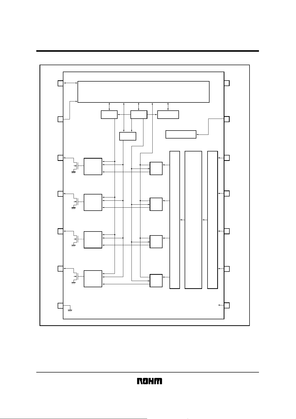
Block diagram
!!!!
BU9817FV
SDA
SCL
OD1
OD2
Sel
14 VDD
13 STOPB
12
AD1
11
AD2
1
I2C BUS Interface
Vul
Register
Pointer
Register
Vdl
2
3
4
Reset
Voltage
Hysteresis
Comparator
Reset
Voltage
Hysteresis
Comparator
Register
ADV
Register
ADV
Register
Configuration
Register
Reset & Shutdown
Sel
Reset
Shutdown
8bit
A / D
OD3
OD4
GND
AD3
5
6
7
Reset
Voltage
Hysteresis
Comparator
Reset
Voltage
Hysteresis
Comparator
ADV
Register
ADV
Register
10
AD4
9
CLK
8

Multimedia ICs
Pin descriptions
!!!!
Pin No. Pin name Function
10
11
12
13
14
1
2
3
4
5
6
7
8
9
SDA
SCL
OD1
OD2
OD3
OD4
GND
CLK
AD4
AD3
AD2
AD1
STOPB
DD
V
I2C BUS Serial Data Line
2
C BUS Serial Clock Input
I
Open Drain Output 1
Open Drain Output 2
Open Drain Output 3
Open Drain Output 4
Ground
Clock for Logic Input
Analog-to-Digtal Converter Input 4
Analog-to-Digtal Converter Input 3
Analog-to-Digtal Converter Input 2
Analog-to-Digtal Converter Input 1
Reset & Power save mode set
Supply Voltage 3.0V to 5.5V
BU9817FV

Multimedia ICs
Input / output equivalent circuits
!!!!
Pin. No Pin name Input / output circuits Function
2
I
C BUS serial data input / output.
1
2
SDA
SCL
When only input address accords slave
address (BU9817FV's), register data is
inputted or outputted.
2
I
C BUS serial clock input.
BU9817FV
3
4
5
6
7
8
OD1
OD2
OD3
OD4
GND
CLK
Open-drain output corresponds to AD1 to
AD4 input.
Connect this pin a pull-up resister.
The pull-up resister should be above V
4mA (Ω).
Ground terminal.
Clock input for ADC block.
Input clock is 32.768kHz.
AD converter and voltage hysteresis
comparator use this clock to operate.
DD
/
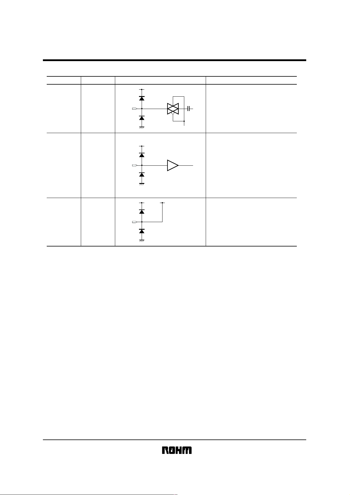
Multimedia ICs
Input / output equivalent circuits
!!!!
Pin. No Pin name Input / output circuits Function
BU9817FV
10
11
12
13
14
9
AD1
AD2
AD3
AD4
STOPB
V
DD
AD input.
Each channel is converted in order.
(AD1, AD2, AD3, AD4, AD1,AD2...)
Reset and power save mode setting.
High: Operation mode
Operation follows the setting of
configuration register.
Low : Reset & Power save mode
Reset the all internal circuit and stop
the ADC operation.
Go into power save mode.
∗
Be sure to set STOPB pin low for initial
reset of the internal circuit, when the
BU9816FV is power up.
Power supply.
Supply voltage 3.0V to 5.5V.
 Loading...