

Page 1
t
(
)
(
)
r
r
p
g
g
p
(
A
)
V
Multifunction LCD Segment Driver
BU97930MUV MAX 108 segments (SEG27×COM4)
●Features
Integrated RAM for display data (DDRAM):
27 x 4 bit (Max 108 Segment)
LCD drive output:
4 Common output, Max 27 Segment output
Integrated 1ch LED driver circuit
Segment /GPO(Max 4port) output mode selectable
Support PWM generation from ext. or internal clock
(Resolution: 8bit)
Support standby mode
Integrated Power-on-Reset circuit (POR)
Integrated Oscillator circuit
No external component
Low power consumption design
Independent power supply for LCD driving
Support Blink function
(Blink frequency 1.6, 2.0, 2.6, 4.0Hz selectable)
●Applications
Telephone
FAX
Portable equipment (POS, ECR, PDA etc.)
DSC
DVC
Car audio
Home electrical appliance
Meter equipment
etc.
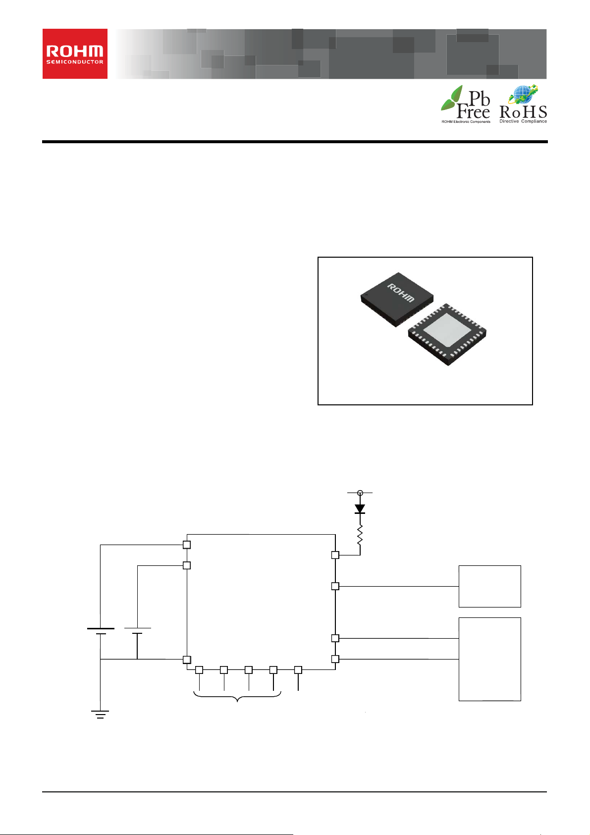
●Ty pical A pplication Circuit
LED/GPO using case
5.0V
3.3V
VSS
VLCD
VDD
BU97930MUV
Input signal from controlle
INHb
●Key Specifications
■ Supply Voltage Range: +1.8V to +3.6V
■ LCD drive power supply Range: +2.7V to +5.5V
■ Operating Temperature Range: -40°C to +85°C
■ Max Segments: 108 Segments
■ Display Duty: Static, 1/3, 1/4 selectable
■ Bias: Static, 1/3
■ Interface: 3wire serial interface
●Package W (Typ.) x D (Typ.) x H (Max.)
QFN040V6060
6.00mm x 6.00mm x 1.00mm
VLED=5.0V
arding resistor value
*Re
Please detect the value accordin
ut current value
in
LED
SEG26
GPO1
to
GPO4
SEG23
to
to
SEG
COM3
22
CLKINCSB SD SCL
CLKIN
*
External CLK input terminal
If not in use, , connect to VSS or o
SEG0
COM0
Datashee
to
current MAX = 20m
Othe
device
LCD
en .
Figure 1. T ypical application circuit
○Product structure:Silicon monolithic integrated circuit ○This product is not designed for protection against radioactive rays.
www.rohm.com
© 2013 ROHM Co., Ltd. All rights reserved.
TSZ22111・14・001
1/28
TSZ02201-0A0A2D300060-1-2
8.Jan.2013 Rev.002
Page 2
Datasheet
BU97930MUV MAX 108 segments (SEG27×COM4)
r
r
(typ=40.96
12345678910302928272625242322
21
Datasheet
●Block Diagram / Pin Configuration / Pin Description
VLCD
LCD voltage
G enerator
COM0……COM3
common
drive
SEG0 …...22 SEG23...26
Segment
driver
LCD
BIAS
SELECTOR
common
counter
blink timing
generator
GPO data latch
divider
(Div.2)
Command
Data
CSB
Decoder
serial inter face
IF FILTER
SD
Power On
Reset
INHb
CLKIN
VDD
VSS
VSS
CR O
OS C block
kHz
DDRAM
SCL
Segment
driver/GPO
Controlle
GPO
LED
LED
drive
PWM
Generator
CSB
SCL
SD
VDD
INHb
CLKIN
VLCD
COM0
COM1
COM2
40
VSS COM3
39
LED SEG0
38
SEG26 SEG1
37
SEG25 SEG2
36
SEG24 SEG3
35
SEG23 SEG4
34
SEG22 SEG5
33
SEG21 SEG6
32
SEG20 SEG7
31
SEG19 SEG8
SEG18
SEG17
SEG16
EXT-PAD
SEG15
SEG14
SEG13
SEG12
SEG11
11
12
13
14
15
16
17
18
19
20
SEG10
SEG9
Figure 2. Block Diagram Figure 3. Pin Configuration (BOTTOM VIEW)
Table 1 Pin Description
Terminal
CSB 1 I - Chip select: "L" active
SCL 2 I - Serial data transfer clock
SD 3 I - Input serial data
VDD 4 - - Power supply for LOGIC
CLKIN 6 I OPEN / VSS
VSS 40 - - GND
VLCD 7 - - Power supply for LCD
INHb 5 I VDD
COM0 to 3 8 to 11 O OPEN COMMON output for LCD
Terminal
number
I/O unused case Function
External clock input terminal (for display/PWM using selectable);
Support Hi-Z input mode at internal clock mode
Display turning on/off select terminal
H: turning on display, L: turning off display
INHb = “L”: All SEG/COM terminals : output VSS level
GPO terminal : output VSS level
LED drive terminal : output Hi-Z
SEG0 to 22 12 to 34 O OPEN SEGMENT output for LCD
SEG23 to 26 35 to 38 O OPEN SEGMENT output for LCD/GPO
LED 39 O OPEN LED driver output
EXT-PAD - - VSS substrate
www.rohm.com
© 2013 ROHM Co., Ltd. All rights reserved.
TSZ22111・15・001
2/28
TSZ02201-0A0A2D300060-1-2
8.Jan.2013 Rev.002
Page 3

Datasheet
BU97930MUV MAX 108 segments (SEG27×COM4)
●Absolute Maximum Ratings (VSS=0V)
Parameter Symbol Ratings Unit Remarks
Power supply voltage 1 VDD -0.3 to +4.5 V Power supply
Power supply voltage 2 VLCD -0.5 to +7.0 V Power supply for LCD
Power Dissipation Pd 0.8*
Input voltage range VIN -0.5 to VDD+0.5 V
Operational temperature range Topr -40 to +85 ℃
Storage temperature range Tstg -55 to +125 ℃
Iout1 5 mA SEG output
Output current
*1 When operated higher than Ta=25℃, subtract 8.0mW per degree. (using ROHM standard board)
(board size: 74.2mm×74.2mm×1.6mm material: FR4 board copper foil: land pattern only).
●Recommended Operating Ratings(Ta=-40°C to +85°C,VSS=0V)
Parameter Symbol
Power supply voltage 1 VDD 1.8 - 3.6 V Power supply
Power supply voltage 2 VLCD 2.7 - 5.5 V Power supply for LCD
Output current Iout4 - - 20 mA Per LED port 1ch
●Electrical Characteristics
DC characteristics (Ta=-40°C to +85°C, VDD=1.8V to 3.6V, VLCD=2.7V to 5.5V, VSS=0)
Parameter Symbol
“H” level input voltage VIH 0.8VDD - VDD V SD, SCL, CSB, CLKIN, INHb
“L” level input voltage VIL VSS - 0.2VDD V SD, SCL, CSB, CLKIN, INHb
Hysteresis width VH - 0.2 - V SCL, INHb, VDD=3.3V, Ta=25°C
“H” level input current IIH1 - - 5 µA
“L” level input current IIL1 -5 - - µA
VOH1
“H” level output voltage
(*2)
“L” level output voltage
(*2)
Current consumption
(*1)
*1 Power save mode 1 and frame inversion setting *2 Iload: In this case, load current from only one port
VOH2
VOH3
VOL1 - - 0.4 V
VOL2 - - 0.4 V
VOL3 - - 0.5 V
VOL4 - 0.11 0.5 V
IstVDD - 3 10 µA
IstVLCD - 0.5 5 µA
IVDD1 - 8 15 µA
IVDD2 - 30 45 µA
IVLCD1 - 10 15 µA
IVLCD2 - 30 48 µA
Iout2 5 mA COM output
Iout3 10 mA GPO output
Iout4 50 mA LED output
Ratings
MIN TYP MAX
Limit
MIN TYP MAX
VLCD
-0.4
VLCD
-0.4
VLCD
-0.6
- - V
- - V
- - V
1
Unit Remarks
Unit Condition
W
SD, SCL, CSB, CLKIN,
INHb, VI=3.6V
SD, SCL, CSB, CLKIN,
INHb, VI=0V
Iload=-50µA, VLCD=5.0V
SEG0 to SEG26
Iload=-50µA, VLCD=5.0V,
COM0 to COM3
Iload=-1mA,VLCD=5.0V,
SEG23 to SEG26(GPO mode)
Iload= 50µA, VLCD=5.0V,
SEG0 to SEG26
Iload= 50µA, VLCD=5.0V,
COM0 to COM3
Iload=1mA, VLCD=5.0V,
SEG23 to SEG26(GPO mode)
Iload=20mA, VLCD=5.0V,
LED
Input terminal ALL’L’,
Display off, Oscillation off
Input terminal ALL’L’,
Display off, Oscillation off
VDD=3.3V, Ta=25°C, 1/3bias, fFR=64Hz,
PWM generate off, All output pin open
VDD=3.3V, Ta=25°C, 1/3bias, fFR=64Hz,
PWM Frequency=500Hz setting,
All output pin open
VLCD=5.0V, Ta=25°C, 1/3bias, fFR=64Hz,
LED generate off, All output pin open
VLCD=5.0V , Ta=25℃, 1/3bias, fFR=64Hz,
PWM Frequency=500Hz setting,
All output pin open
Datasheet
www.rohm.com
© 2013 ROHM Co., Ltd. All rights reserved.
TSZ22111・15・001
3/28
TSZ02201-0A0A2D300060-1-2
8.Jan.2013 Rev.002
Page 4
Datasheet
BU97930MUV MAX 108 segments (SEG27×COM4)
W
f
●Electrical Characteristics – continued
Oscillation Frequency Characteristics (Ta=-40°C to +85°C, VDD=1.8V to 3.6V, VLCD=2.7V to 5.5V, VSS=0)
Parameter Symbol
Frame frequency 1 fFR1 57.6 64 70.4 Hz
Frame frequency 2 fFR2 51.2 64 73.0 Hz
Frame frequency 3 fFR3 45.0 - 64 Hz
MPU interface Characteristics (Ta=-40°C to +85°C, VDD=1.8V to 3.6V, VLCD=2.7V to 5.5V, VSS=0)
Parameter Symbol
Input rise time tr - - 50 ns
Input fall time tf - - 50 ns
SCL cycle time tSCYC 250 - - ns
“H” SCL pulse width tSHW 50 - - ns
“L” SCL pulse width tSLW 50 - - ns
SD setup time tSDS 50 - - ns
SD hold time tSDH 50 - - ns
CSB setup time tCSS 50 - - ns
CSB hold time tCSH 50 - - ns
“H” CSB pulse width tCHW 50 - - ns
CSB
SCL
SD
tCSS
t
tSL
tSDS tSDH
MIN MIN MIN
MIN TYP MAX
tSCYC
tSHW
Limit
Limit
Unit Condition
VDD=3.3V, Ta=25°C, fFR=64Hz setting
VDD=2.5 to 3.6V fFR=64Hz setting
VDD=1.8 to 2.5V fFR=64Hz setting
unit Condition
tCSH
tr
Datasheet
tCHW
Figure 4. Serial interface timing
www.rohm.com
© 2013 ROHM Co., Ltd. All rights reserved.
TSZ22111・15・001
4/28
TSZ02201-0A0A2D300060-1-2
8.Jan.2013 Rev.002
Page 5
Datasheet
BU97930MUV MAX 108 segments (SEG27×COM4)
●I/O equivalent circuit
VLCD
VSS
VDD
CSB, SD,
SCL,INHb
CLKIN
VSS
VLCD
SEG23-26
VSS
VDD
VSS
VLCD
SEG0-22
COM0-3
VSS
LED
VSS
Datasheet
www.rohm.com
© 2013 ROHM Co., Ltd. All rights reserved.
TSZ22111・15・001
Figure 5. I/O equivalent circuit
5/28
TSZ02201-0A0A2D300060-1-2
8.Jan.2013 Rev.002
Page 6
Datasheet
BU97930MUV MAX 108 segments (SEG27×COM4)
r
r
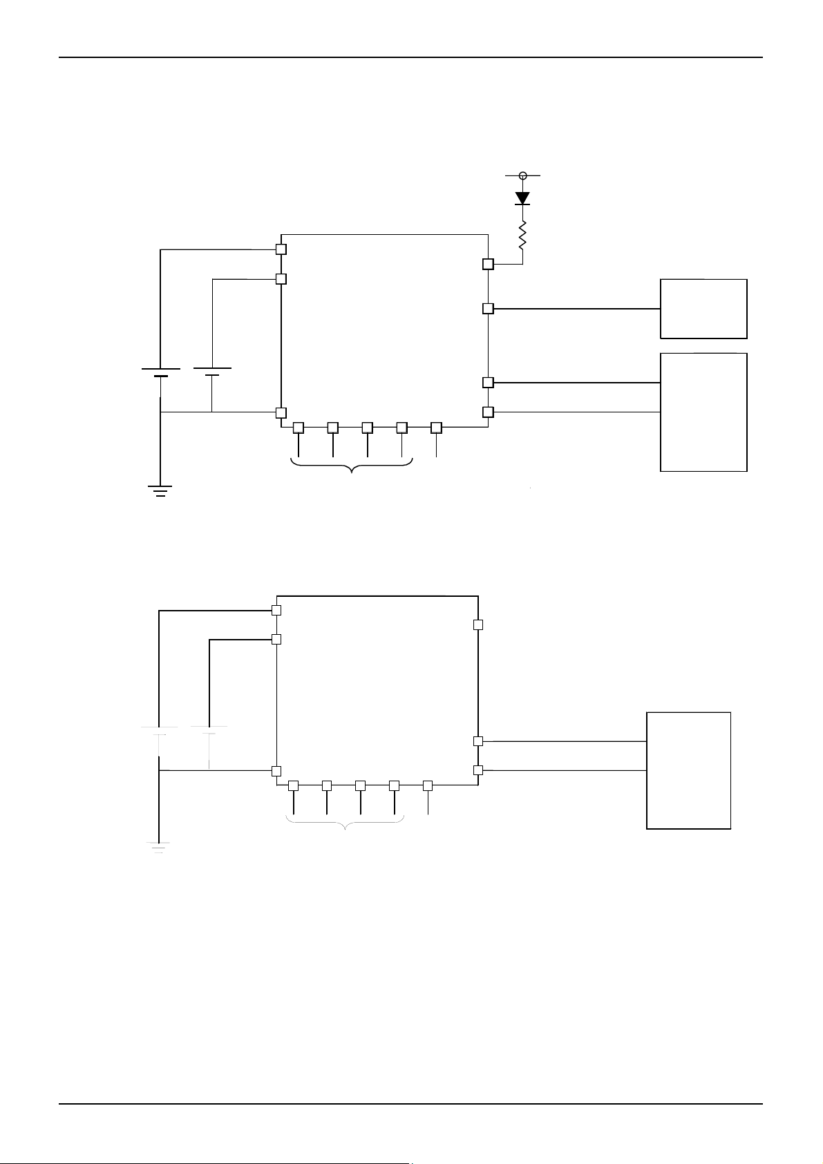
●Example of recommended circuit
1) LED/GPO operation
2) SEG output only operation
5.0 V
3. 3V
VSS
VLCD
VDD
BU97930MUV
Input signal from controlle
INHb
LED
CLKINCSB SD SCL
CLKIN
*
External CLK input terminal
In case being unused, connect to VSS
VLED =5. 0V
*Regarding resistor value
Please detect the value according to
input current value (
SEG26(GPO
to
SEG0
COM0 to COM3
1)
SEG23( GPO 4)
SEG22
to
Datasheet
current MAX = 20mA)
Othe
device
LCD
or be opened
.
VLCD
LED
VDD
OPEN if unused
BU97930MUV
5.0V 3.3V
VSS
Input signal from controller
INHb
CLKINCSB SD SCL
CLKIN
*
External CLK input terminal
connect to VSS or open. If unused
SEG0
COM0toCOM3
Figure 6. Example of Recommended Circuit
to
SEG26
LCD
www.rohm.com
© 2013 ROHM Co., Ltd. All rights reserved.
TSZ22111・15・001
6/28
TSZ02201-0A0A2D300060-1-2
8.Jan.2013 Rev.002
Page 7
Datasheet
BU97930MUV MAX 108 segments (SEG27×COM4)
CD/C
3
0
4D6D5
2
Datasheet
●Function description
○Command and data transfer method
○3-SPI (3-wire serial interface)
This device is controlled by a 3-wire signal (CSB, SCL, and SD).
First, Interface counter is initialized with CSB=“H".
Setting CSB=”L”, enables SD and SCL inputs.
The protocol of 3-SPI transfer is as follows.
Each command starts with Command or Data judgment bit (D/C) as MSB data,
followed by data D6 to D0 (this is when CSB =”L”).
(Internal data is latched at the rising edge of SCL, serial data is converted to an 8-bit parallel data at the falling edge of
the 8th CLK.)
When CSB changes from “L” to “H”, and at this time serial commands are less than 8 bits, command and data transfers
are cancelled. To start sending command again, please set CSB=”L" and send command continuously.
After sending RAMWR or BLKWR or GPOSET command, this device is in the RAM data input mode. Under this mode,
device can not accept new commands.
In this case, execute a “H” to “L” transition at CSB, after this sequence, the device is released from RAM data input mode,
and can accept new command.
CSB
1st byte Command 2nd byte Command
3rd byte Command
SCL
SD
D/C
D3 D6D0 D0
D
D2
D/
D1 D
D5
D6D5D4D
D/CD4 D3 D2 D1
D1 D
D6
Figure 7. 3-SPI Data transfer Format
* 8-bit data, sending after RAMWR command, are display RAM data
* 8-bit data, sending after BLKWR command, are blink RAM data
* SCL and SD can be set to “H” or cleared to “L” during CSB=”H”.
www.rohm.com
© 2013 ROHM Co., Ltd. All rights reserved.
TSZ22111・15・001
7/28
TSZ02201-0A0A2D300060-1-2
8.Jan.2013 Rev.002
Page 8
Datasheet
BU97930MUV MAX 108 segments (SEG27×COM4)
A
A
A
A
j
Datasheet
○Write display data and transfer method
This device has Display Data RAM (DDRAM) of 28×4=112bit.
The relationship between data input and display data, DDRAM data and address are as follows.
Command
1st Byte
10000011
ddress set
2nd Byte
Command
00000000
Command
10100000
RAM Write
a
b
Display RAM data
c
de
g
h
f
i
kl m
no
…
p
According to this command, an 8-bit binary data will be written to the DDRAM. The starting address of the DDRAM where
data will be written is specified by “ADSET” command, and is automatically incremented for every 4 bits of data received..
Writing data to DDRAM can be done by continuously sending data.
(In case data is sent continuously after write date at 1Ah (SEG26), RAM data will be written to 1Bh (dummy address)
and return to address 00h (SEG0) automatically.)
In case SEG port assigned to GPO port by OUTSET command, corresponding SEG address do not change and used as
dummy address.
DDRAM address
00 01 02 03 04 05 06 07
・・・
0 a e i m
1 b f j n
2 c g k o
BIT
3 d h l p
SEG
SEG
0
1
SEG
2
SEG
3
SEG4SEG5SEG6SEG
・・・
7
19h 1Ah 1Bh
SEG
25
SEG
26
ADDRESS
DUMMY
Display data write to DDRAM every 4 bits.
In case CSB changes from ”L” to ”H” before 4 bits of data transfer was finished, RAM write is cancelled.
Command
Display data
CSB
1st byte Command / 2nd byte Command
COM0
COM1
COM2
COM3
SCL
SD D2 D5 D4 D3 D2 D1 D0
Internal
signal
RAM write
Address set command RAMWR command
Command
RAMWR command
CSB
SCL
Internal
signal
RAM write
1st byte Command / 2nd byte Command
Address set command
D6 D5 D4 D3D7 D1
ddress 00h
D7 D6SD
D4 D3 D2 D0
Address 00h
ddress 01h
RAM write every 4bit
Address 30h
D0 D7
D6
ddress 02h
Display data
D7
Address 31h
data lower than 4bit case
RAM write is canceled
D5
D5 D6
D4D4 D2 D1D5 D3
Addres00h
Auto increment
Return to address 00h
Figure 8. Display Data Transfer Method
www.rohm.com
© 2013 ROHM Co., Ltd. All rights reserved.
TSZ22111・15・001
8/28
TSZ02201-0A0A2D300060-1-2
8.Jan.2013 Rev.002
Page 9

Datasheet
BU97930MUV MAX 108 segments (SEG27×COM4)
○Blink function
This device has Blink function. Blink function can set each segment port individually.
Blink ON/OFF and Blink frequency are set by the BLKSET command.
Blink frequency varies according to fCLK characteristics.
Blink setup of each segment is controlled by BLKWR command.
The write start address is specified by “BLKADSET” command. And this address will automatically increment every 4 bits
of blink data received. The relation of BLKWR command, blink ram data, and blinking segment port is below.
In case data is “1”, segment will blink, on the other hand when data is “0”, segment will not blink.
(In case data is written continuously after write data at 1Ah (SEG26), RAM data will be written to 1Bh (dummy address)
and return to address 00h (SEG0) automatically.)
Please refer to the following figures about Blink operation of each segment.
In case SEG port assigned to GPO port by OUTSET command, corresponding SEG address does not change and used
as dummy address.
1st Byte
Command
10000100
Command
Blink set
2nd Byte
00000011
1st Byte
Command
10000111
2nd Byte
Command
00000000
Blink Address set
Command
11000000
Blink
RAMWR
a
b
d
c
Blink RAM data
g
f
e
h i
j
k
m
n o
l
Blink RAM address
00 01 02 03 04 05 06 07
0 a e i m
・・・
19h 1Ah 1Bh
ADDRESS
DUMMY
1 b f j n COM1
2 c g k o COM2
BIT
3 d h l p COM3
SEG 0 SEG 1 SEG 2 SEG 3 SEG4 SEG5 SEG6 SEG
7
SEG
25
SEG
26
Datasheet
…
p
COM0
DDRAM data
SEG A SEG B SEG C SEG D
Blink RAM data
SEG A SEG B SEG C SEG D
Segment output
SEG A SEG B SEG C SEG D SEG A SEG B SEG C SEG D SEG A SEG B SEG C SEG D SEG A SEG B SEG C SEG D
under the 2Hz stting segment output will blink every 0.5 second (ON->OFF->ON)
www.rohm.com
© 2013 ROHM Co., Ltd. All rights reserved.
TSZ22111・15・001
Blink frequency
Figure 9. Blink Operation
9/28
SEGA/B is blink
TSZ02201-0A0A2D300060-1-2
8.Jan.2013 Rev.002
Page 10

Datasheet
BU97930MUV MAX 108 segments (SEG27×COM4)
○LCD Driver Bias/Duty Circuit
BU97930MUV generates LCD driving voltage using an on-chip Buffer AMP.
Also, it can drive LCD with low power consumption
*Line and frame inversion can be set by MODESET command.
*1/4duty, 1/3duty and static mode can be set by DISCTL command.
About each LCD driving waveform, please refer to “LCD driving waveform” descriptions.
○Initial state
Initial state after SWRST command input
○Display off
○All command register values are in Reset state.
○DDRAM address data and Blink address data are initialized
(DDRAM data and Blink RAM data are not initializing.
Please write DDRAM data and Blink RAM data before Display on.)
●Command / Function list
Function description table
NO Command Function
1 Mode Set (MODESET) Sets LCD drive mode (display on/off, current mode)
2 Display control (DISCTL)
3 Address set (ADSET)
4 Blink set (BLKSET)
5 Blink address set (BLKADSET)
SEG/GPO port change
6
(OUTSET)
LED drive control (PWMSET)
7
(H piece adjustment of PWM)
8 RAM WRITE (RAMWR) Writes display data to display data RAM
9 Blink RAM WRITE (BLKWR) Writes Blink data to BLINK data RAM
10 All Pixel ON (APON) Sets all Pixel display on
11 All Pixel OFF (APOFF) Sets all Pixel display off
12 All Pixel On/Off mode off (NORON)
13 Software Reset (SWRST) Software Reset
14
OSC external input (OSCSET)
15 GPO output set (GPOSET) Sets GPO output data
Sets LCD drive mode
(frame freq., line/frame inversion)
Sets display data RAM address for RAMWR command
Sets Blink mode on/off
Sets Blink data RAM address for BLKWR command
Selects segment output/general purpose output (GPO)
Sets PWM1 signal “H” width for LED driving
Sets normal display mode (APON/APOFF cancel)
Enables External clock input
Datasheet
www.rohm.com
© 2013 ROHM Co., Ltd. All rights reserved.
TSZ22111・15・001
10/28
TSZ02201-0A0A2D300060-1-2
8.Jan.2013 Rev.002
Page 11

Datasheet
BU97930MUV MAX 108 segments (SEG27×COM4)
●Command Descriptions
D/C, Data / Command judgment bit (MSB)
For more details, please refer to 3wire serial I/F
○Mode Set (MODESET)
MSB LSB
D/C D6 D5 D4 D3 D2 D1 D0 Hex Reset
1st byte command 1 0 0 0 0 0 0 1 81h 2nd byte command 0 0 0 0 P3 P2 P1 P0 - 00h
Display Set
Condition P3 Reset state
Display OFF 0 ○
Display ON 1
Display OFF : No LCD driving mode (Output: VSS Level)
Turn off OSC circuit and LCD power supply circuit. (Synchronized with frame freq)
Display ON : LCD driving mode
Turn on OSC circuit and LCD power supply circuit.
Read data from DDRAM and display to LCD.
LED port and GPO port output states are not affected by a Display on/off state
Output state is determined by command setup (OUTSET GPOSET, PWMSET) and INHb terminal state,
respectively. For more details, please refer to each command description.
LCD drive mode set
Condition P2 Reset state
Frame inversion 0 ○
Line inversion 1
Current mode set
Condition P1 P0 Reset state
Power save mode1 0 0 ○
Power save mode2 0 1
Normal mode 1 0
High power mode 1 1
* Please supply the VLCD voltage larger than 3V at High power mode.
(Reference data of consumption current)
Condition Current consumption
Power save mode 1 ×1.0
Power save mode 2 ×1.7
Normal mode ×2.7
High power mode ×5.0
* The value changes according to the panel load.
Datasheet
www.rohm.com
© 2013 ROHM Co., Ltd. All rights reserved.
TSZ22111・15・001
11/28
TSZ02201-0A0A2D300060-1-2
8.Jan.2013 Rev.002
Page 12

Datasheet
BU97930MUV MAX 108 segments (SEG27×COM4)
○Display control (DISCTL)
MSB LSB
D/C D6 D5 D4 D3 D2 D1 D0 Hex Reset
1st byte Command 1 0 0 0 0 0 1 0 82h 2nd byte Command 0 0 0 0 P3 P2 P1 P0 - 02h
Duty set
Condition P3 P2 Reset state
1/4duty (1/3bias) 0 0 ○
1/3duty (1/3bias) 0 1
Static (1/1bias) 1 *
*: Don’t care
In 1/3 duty, Display data and Blink data of COM3 are ineffective.
COM1 and COM3 output are same data.
Please be careful in transmitting display data and blink data.
The examples of SEG/COM output waveform, under each Bias/Duty set up, are sho wn at "LCD Driver Bias/Duty
Circuit" description.
Frame frequency set
Condition
(1/4,1/3,1/1duty)
(128Hz, 130Hz, 128Hz) 0 0
(85Hz, 86hz, 64Hz) 0 1
(64Hz, 65Hz, 48Hz) 1 0 ○
(51Hz, 52Hz, 32Hz) 1 1
Relation table, between Frame frequencies (FR), integrated oscillator circuit (OSC) and Divide number.
DISCTL
(P1,P0)
(0,0) 160 156 160 128 131.3 128
(0,1) 240 237 320 85.3 86.4 64
(1,0) 320 315 428 64 65 47.9
(1,1) 400 393 640 51.2 52.1 32
*1: FR is frame frequency, in case OSC frequency = 20.48KHz (typ).
The Formula, to calculate OSC frequency from Frame frequency is shown below.
“ OSC frequency = Frame frequency (measurement value) x Divide number ”
Divide number:Please determine by using the value of Frame Frequency Set (P1,P0) and duty setting (P3,P2).
Ex) (P1,P0) = (0,1) ,(P3,P2) = (0,1) => Divide number= 237
(0,0)
1/4duty
P1 P0 Reset state
Divide FR [Hz] (*1)
Duty set (P3,P2) Duty set (P3,P2)
(0,1)
1/3duty
(1,*)
1/1duty
(0,0)
1/4duty
(0,1)
1/3duty
Datasheet
(1,*)
1/1duty
www.rohm.com
© 2013 ROHM Co., Ltd. All rights reserved.
TSZ22111・15・001
12/28
TSZ02201-0A0A2D300060-1-2
8.Jan.2013 Rev.002
Page 13

Datasheet
BU97930MUV MAX 108 segments (SEG27×COM4)
○Address set (ADSET)
MSB LSB
MSB D/C D6 D5 D4 D3 D2 D1 D0 Hex Reset
1st byte Command 1 0 0 0 0 0 1 1 83h 2nd byte Command 0 0 0 P4 P3 P2 P1 P0 - 00h
Set start address to write DDRAM data.
The address can be set from 00h to 1Ah. (Address 1Bh is used at dummy address)
Do not set other addresses. (Except 00h to 1Bh address is not acceptable.)
In case writing data to DDRAM, make sure to send RAMWR command.
○Blink set (BLKSET)
MSB LSB
D/C D6 D5 D4 D3 D2 D1 D0 Hex Reset
1st byte Command 1 0 0 0 0 1 0 0 84h 2nd byte Command 0 0 0 0 0 P2 P1 P0 - 00h
Set Blink ON/OFF.
For more details, please refer to "Blink function".
Blink set
Blink mode(Hz) P2 P1 P0 Reset state
OFF 0 0 / * 0 / * ○
1.6 1 0 0
2.0 1 0 1
2.6 1 1 0
4.0 1 1 1
*: Don’t care
○Blink address set (BLKADSET)
MSB LSB
D/C D6 D5 D4 D3 D2 D1 D0 Hex Reset
1st byte Command 1 0 0 0 0 1 1 1 87h 2nd byte Command 0 0 0 P4 P3 P2 P1 P0 - 00h
Set Blink data RAM start write address.
The address can be set from 00h to 1Ah. (Address 1Bh is used at dummy address)
Do not set other addresses. (Except 00h to 1Bh address is not acceptable.)
In case writing data to Blink RAM, make sure to send BLKWR command
Datasheet
www.rohm.com
© 2013 ROHM Co., Ltd. All rights reserved.
TSZ22111・15・001
13/28
TSZ02201-0A0A2D300060-1-2
8.Jan.2013 Rev.002
Page 14

Datasheet
BU97930MUV MAX 108 segments (SEG27×COM4)
○SEG/GPO port change (OUTSET)
MSB LSB
D/C D6 D5 D4 D3 D2 D1 D0 Hex Reset
1st byte Command 1 0 0 0 1 0 0 0 88h 2nd byte Command 0 0 0 0 0 P2 P1 * - 00h
Set output mode, Segment output or GPO output.
P2 to P0: Select changing port number. (SEG23 to SEG26 ports are SEG mode/GPO mode selectable)
In case GPO output is selected, Terminal output data is set by GPOSET command.
Ex) In case SEG 26 port assigned to GPO,
If GPO1 data is "H", GPO1 (SEG26) port outputs "H" (VLCD Level).
If GPO1 data is "L", GPO1 (SEG26) port outputs "L" (VSS level).
Output terminal state under the P2 to P0 set condition is listed below
Output Terminal state
Condition SEG Terminal state (SEG output/GPO output)
P2 P1 P0 SEG23 port SEG24 port SEG25 port SEG26 port
0 0 * SEG23 SEG24 SEG25 SEG26
0 1 0 SEG23 SEG24 SEG25 GPO1
0 1 1 SEG23 SEG24 GPO2 GPO1
1 0 0 SEG23 GPO3 GPO2 GPO1
1 0 1 GPO4 GPO3 GPO2 GPO1
1 1 * (OUTSET command will be canceled)
In case SEG port is switched to the GPO port, DDRAM address and Blink RAM address do not change.
In this case DDRAM address and Blink RAM address, selected GPO output mode is dummy address.
The output state of GPO and LED port under the INHb H/L, display on/off, and RESET state are listed below.
Control port
INHb DISPLAY
H L ON OFF
Datasheet
RESET state
According to
GPO
LED
www.rohm.com
© 2013 ROHM Co., Ltd. All rights reserved.
TSZ22111・15・001
GPOSET
command
According to
PWMSET
command
Low Fix
Hi-Z
14/28
According to
GPOSET
command
According to
PWMSET
command
According to
GPOSET
command
According to
PWMSET
command
GPO unselected
(All SEG output)
LED unselected
(All SEG output)
TSZ02201-0A0A2D300060-1-2
8.Jan.2013 Rev.002
Page 15

Datasheet
BU97930MUV MAX 108 segments (SEG27×COM4)
○LED drive-control (PWM “H” width control) command (PWMSET)
MSB LSB
D/C D6 D5 D4 D3 D2 D1 D0 Hex Reset
1st byte Command 1 0 0 0 1 0 1 0 8Ah 2nd byte Command 0 0 0 0 0 0 P7 P6 - 00h
3rd byte Command 0 0 P5 P4 P3 P2 P1 P0 - 00h
2nd and 3rd byte command data are able to set from 00h to 3Fh (described as 8bit binary data).
In case other value is selected, sending command is ignored, and 2nd and 3rd byte command data is set to 3Fh.
In default state, 2nd and 3rd byte command data are set to 00h.
In case command is less than 3 bytes, sending command is cancelled.
According to PWMSET command, LED driving signal is adjustable. PWM “H” width is adjustable by 8-bit resolution.
Explanation about P7 to P6 data of 2nd byte command and P5 to P0 data of 3rd byte command are as follows:
(The 2nd byte data are used as upper 2bit, and 3rd byte data are used as lower 6 bits.)
8bit mode: P7 data is used as MSB of 8 bits, and P0 data is used LSB.
LED driving period is decided by the “H” width of PWM signal, generated by PWM generator circuit (resolution: 8 bits).
Ex)
In case, external PWM clock 125KHz, parameter setting value is 127 ( 7Fh )
1-bit resolution: 8us
ALL HI set: PWM signal frequency about 500Hz, H width about 2.00msec
ALL LOW set: PWM signal frequency about 500Hz, H width 0usec (in case 8-bit resolution)
This command is reflected, synchronizing with a next PWM frame head.
And, LED port output is as follows. LED port operation does not affect Display ON/OFF state.
(*) About the PWM frequency and PWM “H” width calculation.
PWM cycle and PWM “H” width, decided by PWM clock cycle are described as follows:
(PWM clock cycle is a minimum unit of PWM “H” width)
In case PWM is generated from internal clock, the PWM cycle varies according to OSC frequency.
PWM (ALL HI)
PWM (ALL Low)
PWM frequency = PWM clock cycle × (Number of the steps (8bit =256) - 1 )
PWM H width = PWM clock cycle × Parameter set value (8bit: 0 to 255)
PWM Duty = PWM H width/PWM cycle = Parameter set value / Number of the steps
Duty shift
FFh
(H width : wide)
00h
(H width: narrow)
Datasheet
www.rohm.com
© 2013 ROHM Co., Ltd. All rights reserved.
TSZ22111・15・001
15/28
TSZ02201-0A0A2D300060-1-2
8.Jan.2013 Rev.002
Page 16

Datasheet
BU97930MUV MAX 108 segments (SEG27×COM4)
○RAM WRITE (RAMWR)
MSB LSB
D/C D6 D5 D4 D3 D2 D1 D0 Hex Reset
1st byte Command 1 0 1 0 0 0 0 0 A0h 2nd byte Command Display data Random
….
n byte Command Display data Random
Input data, sending after 1st byte command, are used as Display data. And display data are sent every 4 bits. Please set
this command after the ADSET command.
○Blink RAM WRITE (BLKWR)
MSB LSB
D/C D6 D5 D4 D3 D2 D1 D0 Hex Reset
1st byte Command 1 1 0 0 0 0 0 0 C0h 2nd byte Command Blink data Random
….
n byte Command Blink data Rand om
Input data, sending after 1st byte command, are used as Display data. And display data are sent every 4 bits.
Please set this command after the BLKADSET command.
○All Pixel ON (APON)
MSB LSB
D/C D6 D5 D4 D3 D2 D1 D0 Hex Reset
1st byte Command 1 0 0 1 0 0 0 1 91h -
After sending the command, all SEG outputs set display on state regardless of the DDRAM data.
(This command affects the SEG output terminals only (except GPO and LED output)
○All Pixel OFF (APOFF)
MSB LSB
D/C D6 D5 D4 D3 D2 D1 D0 Hex Reset
1st byte Command 1 0 0 1 0 0 0 0 90h -
After sending the command, all SEG outputs set display off state regardless of the DDRAM data.
(This command affects the SEG output terminals only (except GPO and LED output)
○All Pixel ON/OFF mode off (NORON)
MSB LSB
D/C D6 D5 D4 D3 D2 D1 D0 Hex Reset
1st byte Command 1 0 0 1 0 0 1 1 93h -
After sending the command, all SEG outputs are released from APON/APOFF state.
And SEG port output signal follows DDRAM data.
(This command affects the SEG output terminals only (except GPO and LED output)
After reset sequence or SWRESET, all outputs set NORON state.
○Software Reset (SWRST)
MSB LSB
D/C D6 D5 D4 D3 D2 D1 D0 Hex Reset
1st byte Command 1 0 0 1 0 0 1 0 92h -
After sending the command, device is set to default state.
Datasheet
www.rohm.com
© 2013 ROHM Co., Ltd. All rights reserved.
TSZ22111・15・001
16/28
TSZ02201-0A0A2D300060-1-2
8.Jan.2013 Rev.002
Page 17

Datasheet
BU97930MUV MAX 108 segments (SEG27×COM4)
○OSC external input command (OSCSET)
MSB LSB
D/C D6 D5 D4 D3 D2 D1 D0 Hex Reset
1st byte Command 1 0 0 1 1 0 0 0 98h 2nd byte Command 0 0 0 0 0 P2 P1 P0 - 00h
Sets the type of clock mode. There are 4 selectable modes including external clock input mode.
Details of this command function are as follows.
Condition P2 P1 P0 Reset state
Internal CLK (PWM generation OFF) 0 0 0 ○
External CLK input for PWM (PWM generation OFF) 0 0 1
Internal CLK (PWM generation ON) 0 1 0
External CLK input for PWM (PWM generation ON) 0 1 1
External CLK input for Display (ROHM use only) 1 * *
(P2,P1,P0)=(0,0,1) : External PWM input mode
CLKIN:external PWM input available.
PWMOUT: “L” Output
*under the (P2,P1,P0)=(0,0,0) condition PWMOUT into same state
(P2,P1,P0)=(0,1,0) : PWM is generated from an internal oscillating frequency
(P2,P1,P0)=(0,1,1) : PWM is generated from an External CLK input CLKIN
PWM width is set by PWMSET command.
The relation of OSC function control by each command is as follows:
CLKIN terminal
External clock
External PWM
Integrated OSC
OSCSET
command
PWM
generation
PWMSET
command
Datasheet
(*: Don’t care)
LED
www.rohm.com
© 2013 ROHM Co., Ltd. All rights reserved.
TSZ22111・15・001
Figure 10. OSC External Input
17/28
TSZ02201-0A0A2D300060-1-2
8.Jan.2013 Rev.002
Page 18

Datasheet
BU97930MUV MAX 108 segments (SEG27×COM4)
○GPO output set command (GPOSET)
MSB LSB
D/C D6 D5 D4 D3 D2 D1 D0 Hex Reset
1st byte Command 1 0 0 1 1 0 1 0 9Ah 2nd byte Command 0 0 0 P4 P3 P2 P1 0 - 00h
(*: Don’t care)
Set GPO output data. The relation between SEG port (GPO port) and data is shown below.
GPOSET data GPO port SEG port
P1 GPO1 SEG26
P2 GPO2 SEG25
P3 GPO3 SEG24
P4 GPO4 SEG23
GPO data output is asynchronous from frame cycle.
In case INHb=”H”, GPO output signal follows GPOSET data, on the other hand, in case INHb=”L” GPO output is
GND level. GPO output is not affected by Display ON/OFF state.
Datasheet
www.rohm.com
© 2013 ROHM Co., Ltd. All rights reserved.
TSZ22111・15・001
18/28
TSZ02201-0A0A2D300060-1-2
8.Jan.2013 Rev.002
Page 19

Datasheet
BU97930MUV MAX 108 segments (SEG27×COM4)
A
A
A
A
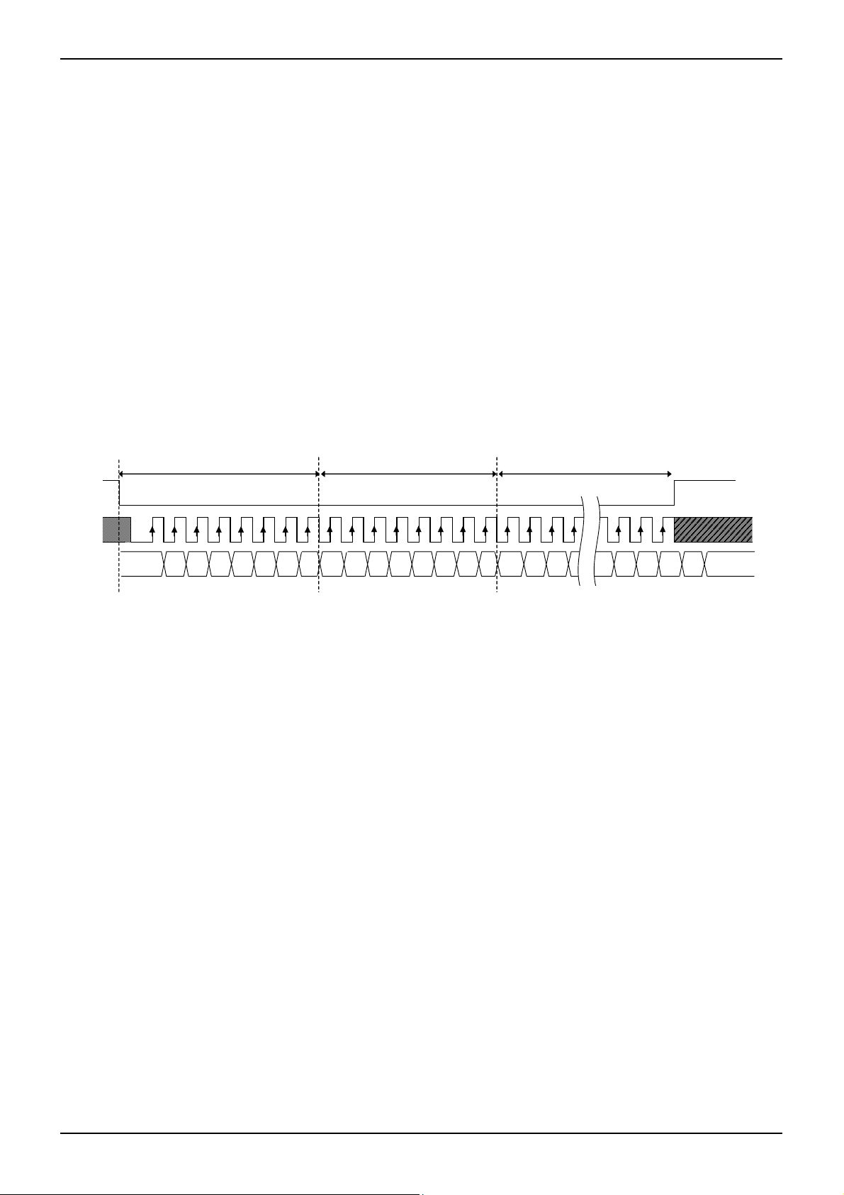
●LCD driving waveform
1/4Duty
Line inversion Frame inversion
SEGn SEGn+1
SEGn+2
SEGn+3
SEGn
SEGn+1
SEGn+2
SEGn+3
Datasheet
state
COM0
COM1
COM2
COM3
Vreg
COM0 COM0
VSS
Vreg
COM1 COM1
VSS
Vreg
COM2 COM2
VSS
Vreg
COM3 COM3
VSS
Vreg
SEGn
SEGn
VSS
Vreg
SEGn+1
SEGn+1
VSS
Vreg
SEGn+2
SEGn+2
VSS
Vreg
SEGn+3
SEGn+3
VSS
Vreg
stateB
1frame 1frame
COM0 state
COM1 stateB
COM2
COM3
Vreg
VSS
Vreg
VSS
Vreg
VSS
Vreg
VSS
Vreg
VSS
Vreg
VSS
Vreg
VSS
Vreg
VSS
Vreg
state
(COM0-SEGn) (COM0-SEGn)
-Vreg
Vreg
stateB stateB
(COM1-SEGn)
(COM1-SEGn)
-Vreg
state
-Vreg
Vreg
-Vreg
Figure 11. Waveform of Line Inversion Figure12. Waveform of Frame Inversion
www.rohm.com
© 2013 ROHM Co., Ltd. All rights reserved.
TSZ22111・15・001
19/28
TSZ02201-0A0A2D300060-1-2
8.Jan.2013 Rev.002
Page 20

Datasheet
BU97930MUV MAX 108 segments (SEG27×COM4)
A
A
A
A
1/3Duty
Line inversion Frame inversion
SEGn SEGn+1
state
COM0
COM1
stateB
SEGn+2
SEGn+3
SEGn SEGn+1
COM0 state
COM1 stateB
Datasheet
SEGn+2 SEGn+3
COM2
COM3
Vreg
COM0 COM0
VSS
Vreg
COM1 COM1
VSS
Vreg
COM2 COM2
VSS
Vreg
COM3 COM3
VSS
Vreg
SEGn SEGn
VSS
Vreg
When
1/3duty
COM3 and COM1 is same
1frame 1frame
When 1/3duty
COM3 and COM1
is same
Vreg
VSS
Vreg
VSS
Vreg
VSS
Vreg
VSS
Vreg
VSS
Vreg
COM2
COM3
When 1/3duty
COM3 and COM1 is same
SEGn+1 SEGn+1
VSS
Vreg
SEGn+2
SEGn+2
VSS
Vreg
SEGn+3
SEGn+3
VSS
Vreg
state
(COM0-SEGn) (COM0-SEGn)
-Vreg
Vreg
stateB stateB
(COM1-SEGn) (COM1-SEGn)
-Vreg
state
VSS
Vreg
VSS
Vreg
VSS
Vreg
-Vreg
Vreg
-Vreg
Figure 13. Waveform of Line Inversion Figure 14. Waveform of Frame Inversion
www.rohm.com
© 2013 ROHM Co., Ltd. All rights reserved.
TSZ22111・15・001
20/28
TSZ02201-0A0A2D300060-1-2
8.Jan.2013 Rev.002
Page 21

Datasheet
BU97930MUV MAX 108 segments (SEG27×COM4)
A
A
A
A
1/1Duty (Static)
Line inversion Frame inversion
SEGn SEGn+1
Datasheet
SEGn SEGn+1SEGn+2 SEGn+3
SEGn+2 SEGn+3
stateB stateB
state
COM0
COM1
COM2
COM3
Vreg
COM0 COM0
VSS
Vreg
COM1 COM1
VSS
Vreg
COM2 COM2
VSS
Vreg
COM3 COM3
VSS
Vreg
When 1/1duty (Static)
COM1 / COM0 is same
waveform
COM2 / COM0 is same
1frame 1frame
waveform
When 1/1duty
(Static)
COM1 / COM0
is same
waveform
COM2 / COM0
is same
waveform
COM3 / COM0
is same
waveform
Vreg
VSS
Vreg
VSS
Vreg
VSS
Vreg
VSS
Vreg
COM0 state
COM1
COM2
COM3
When 1/1duty (Static)
COM1 / COM0 is same
waveform
COM2 / COM0 is same
waveform
SEGn SEGn
VSS
Vreg
SEGn+1 SEGn+1
VSS
Vreg
SEGn+2 SEGn+2
VSS
Vreg
SEGn+3 SEGn+3
VSS
Vreg
state
-Vreg
Vreg
stateB stateB
state
VSS
Vreg
VSS
Vreg
VSS
Vreg
VSS
Vreg
-Vreg
Vreg
-Vreg
-Vreg
Figure 15. Waveform of Line Inversion Figure 16. Waveform of Frame Inversion
www.rohm.com
© 2013 ROHM Co., Ltd. All rights reserved.
TSZ22111・15・001
21/28
TSZ02201-0A0A2D300060-1-2
8.Jan.2013 Rev.002
Page 22

Datasheet
BU97930MUV MAX 108 segments (SEG27×COM4)
●Initialize Sequence
Recommended input sequence is listed below, before starting LCD driving.
(Refer to Power ON/OFF sequence)
Input voltage supply
↓
CSB ‘H’ …interface initializing
↓
CSB ‘L’ …interface command sending
↓
SWRESET …software reset
↓
MODESET …Display off
↓
Various commands setting
↓
RAM WRITE
↓
Blink RAM WRITE
↓
MODESET …Display on
↓
Start LCD driving
*Before initializing sequence, DDRAM address, DDRAM data, Blink address and Blink data are random.
Datasheet
www.rohm.com
© 2013 ROHM Co., Ltd. All rights reserved.
TSZ22111・15・001
22/28
TSZ02201-0A0A2D300060-1-2
8.Jan.2013 Rev.002
Page 23

Datasheet
BU97930MUV MAX 108 segments (SEG27×COM4)
●Cautions on Power-On/ Power-Off condition
○POR circuit
BU97930MUV has “P.O.R” (Power-On Reset) circuit and Software Reset function.
Please follow the recommended Power-On conditions in order to power up properly.
1, Please set power up conditions, follow the recommended tR, tF, tOFF, and Vbot specification below in order to
ensure P.O.R operation.
(*The detection voltage of POR varies because of environment, etc. To operate POR, please satisfy
Vbot lower than 0.5V condition.)
VDD
VDET
tOFF
tR
Recommended condition of tR, tF, tOFF, Vbot
tR tOFF Vbot VDET
Vbot
less than
10ms
* VDET : POR detect level
Over
1ms
less than
0.5V
Figure 17. Power ON/OFF Waveform
Datasheet
TYP
1.2V
2, If it is difficult to meet the above conditions, execute the following sequence after Power-On.
(1) CSB=”L”→”H” condition
(2) After CSB”H”→“L”, execute SWRST command.
In addition, in order to the SWRST command certainly, please wait 1ms after a VDD level reaches to 90% and
CSB=”L”→”H”.
*Before SWRST command, input device will be in unstable state, since SWRST command does not operate
perfect substitution of a POR function.
VDD
CSB
Min 1ms
Min 50ns
SWRST
Command
Figure 18. SWRST Command Sequence
www.rohm.com
© 2013 ROHM Co., Ltd. All rights reserved.
TSZ22111・15・001
23/28
TSZ02201-0A0A2D300060-1-2
8.Jan.2013 Rev.002
Page 24

Datasheet
BU97930MUV MAX 108 segments (SEG27×COM4)
Datasheet
●Power ON / OFF sequence
Display ON/OFF control by INHb terminal is not asynchronous with frame cycle.
In order to prevent display flickering under the power on/off sequence, please send MODESET command (Display off) and
set INHb terminal ="L"
VLCD
VDD
INHb
Command
±0ns No Limit
MODE SET
Display off
Various setupSWRST
REGSET RAM WRITE
Blink RAM
WRITE
MODE SET
Display on
MODE SET
Display off
±0ns No Limit
Figure 19. Power On/Off Sequence
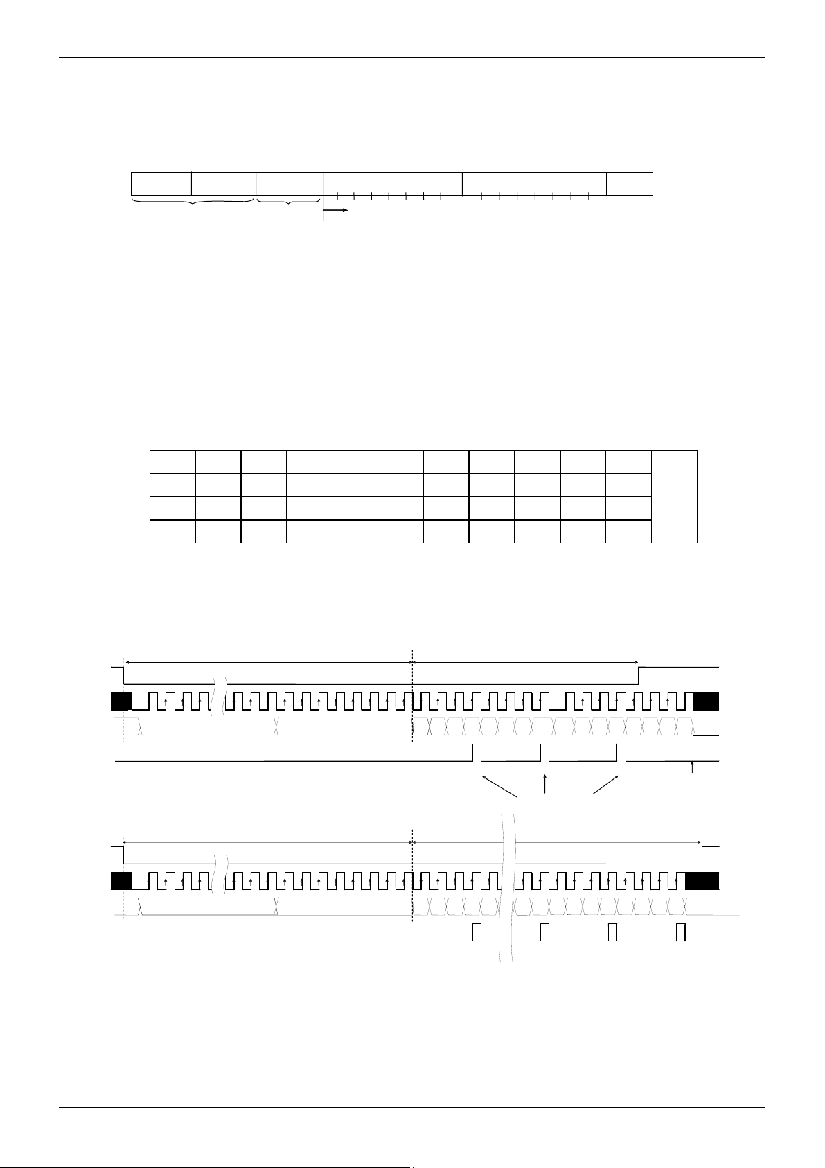
●Notes on pull down resistor usage
Satisfy the following sequence if input terminals are pulled down by external resistors (In case MPU output Hi-Z).
Date transaction period with MPU
CSB
SD
SCL
Input "L"
period
Input"Hi-Z"
period
Figure 20. Recommended sequence when input ports are pulled down
BU97930MUV adopts a 5V tolerant I/O for the digital input. This circuit includes a bus-hold function to keep
HIGH level. A pull down resistor of below 10KΩshall be connected to the input terminals for transitions
from HIGH to LOW because the bus-hold transistor turns on during the input’s HIGH level. (Refer to the
Figure 5; I/O Equivalent Circuit)
A higher resistor than 10KΩ(approximate) causes input terminals being steady by intermediate potential between HIGH
and LOW level so unexpected current is consumed by the system.
The potential depends on the pull down resistance and bus-hold transistor’s resistance.
As the bus-hold transistor turns off upon the input level is cleared to LOW, a higher resistor can be used as a pull down
resistor if MPU sets SD and SCL lines to LOW before it releases the lines.
The LOW period preceding MPU’s bus release shall be at least 50ns as same as a minimum CLK width ( tSLW ).
www.rohm.com
© 2013 ROHM Co., Ltd. All rights reserved.
TSZ22111・15・001
24/28
TSZ02201-0A0A2D300060-1-2
8.Jan.2013 Rev.002
Page 25

Datasheet
BU97930MUV MAX 108 segments (SEG27×COM4)
●Operational Notes
(1) Absolute maximum ratings
Operating the IC over the absolute maximum ratings may damage the IC. The damage can e ither be a short circuit
between pins or an open circuit between pins. Therefore, it is important to consider circuit protection measures, such as
adding a fuse, in case the IC is operated over the absolute maximum ratings.
(2) Recommended operating conditions
These conditions represent a range within which the expected char acteristics of the IC can be approximately o btained.
The electrical characteristics are guaranteed under the conditions of each parameter.
(3) Reverse connection of power supply
Connecting the po wer supply in reverse polarity can damage the IC. Take precautions against reverse polarity when
connecting the power supply, such as mounting an external diode between the power supply and the IC’s power supply
terminals
(4) Power supply lines
Design the PCB layout pattern to provide low impedance ground and supply lines. Separate the ground and supply lines
of the digital and analog blocks to prevent noise in the ground an d supply lines of the digital block from affecting the
analog block. Furthermore, connect a capacitor to ground at all power supply pins. Consider the effect of temperature
and aging on the capacitance value when using electrolytic capacitors.
(5) Ground Voltage
The voltage of the ground pin must be the lowest voltage of all pins of the IC at all operating conditions. Ensure that no
pins are at a voltage below the ground pin at any time, even during transient condition.
Datasheet
(6) Short between pins and mounting errors
Be careful when mounting the IC on printed circuit boards. The IC may be damaged if it is mounted in a wrong
orientation or if pins are shorted together. Short circuit may be caused by conductive particles caught between the pins.
(7) Operation under strong electromagnetic field
Operating the IC in the presence of a strong electromagnetic field may cause the IC to malfunction.
(8) Testing on application boards
When testing the IC on an application board, connecting a c apacitor directly to a low-impedance output p in may subject
the IC to stress. Always discharge capacitors completely after each process or step. The IC’s power supply should
always be turned off completely before connecting or removing it from the test setup during the inspection process. To
prevent damage from static discharge, ground the IC during assembly and use similar precautions during transport and
storage.
(9) Regarding input pins of the IC
In the construction of this IC, P-N junctions are inevitably formed creating parasitic diodes or transistors. The operation
of these parasitic elements can result in mutual interference among circuits, operational faults, or physical damage.
Therefore, conditions which cause these parasitic elements to operate, such as applying a voltage to an input pin lower
than the GND voltage should be avoided. Furthermore, do not apply a v oltage to the input terminals when no power
supply voltage is applied to the IC. Even if the power supply voltage is applied, make sure that the in put terminals have
voltages within the values specified in the electrical characteristics of this IC.
(10) GND wiring pattern
When using both small-signal and large-current GND traces , the two ground traces should be routed separately but
connected to a single ground at the reference point of the applic ation board to avoid fluctuations in the small-signal
ground caused by large currents. Also ensure that the GND traces of external compone nts do not cause variations on
the GND voltage. The power supply and ground lines must be as short and thick as possible to reduce line impedance.
(11) External Capacitor
When using a ceramic capacitor, determine the dielectric constant considering the change of capacitance with
temperature and the decrease in nominal capacitance due to DC bias and others.
(12) Unused input terminals
Input terminals of an IC are often connected to the gate of a CMOS transistor. The gate has extremely high impeda nce
and extremely low capacitance. If left unconnected, the electric field from the outside can easily charge it. The small
charge acquired in this way is enough to produce a signific ant effect on the conduction through the transistor an d cause
unexpected operation of IC. So unless otherwise specified, input terminals not bei ng used should be connected to the
power supply or ground line.
(13) Rush current
When power is first supplied to the IC, rush current may flow instantaneously. It is possible that the charge current to the
parasitic capacitance of internal photo diode or the internal logic may be unstable. Therefore, give special consideration
to power coupling capacitance, power wiring, width of GND wiring, and routing of connections.
www.rohm.com
© 2013 ROHM Co., Ltd. All rights reserved.
TSZ22111・15・001
25/28
TSZ02201-0A0A2D300060-1-2
8.Jan.2013 Rev.002
Page 26

Datasheet
BU97930MUV MAX 108 segments (SEG27×COM4)
●Ordering Information
B U 9 7 9 3 0 M U V - E 2
Part Number
●Marking Diagram
VQFN040V6060 (TOP VIEW)
BU97930
MUV :VQFN040V6060
Part Number Marking
LOT Number
1PIN MARK
Package
Packaging and forming specification
E2: Embossed tape and reel
VQFN040V6060)
(
Datasheet
www.rohm.com
© 2013 ROHM Co., Ltd. All rights reserved.
TSZ22111・15・001
26/28
TSZ02201-0A0A2D300060-1-2
8.Jan.2013 Rev.002
Page 27

Datasheet
BU97930MUV MAX 108 segments (SEG27×COM4)
●Physical Dimension, Tape and Reel Information
Package Name VQFN040V6060
<Tape and Reel information>
Embossed carrier tapeTape
Quantity
Direction
of feed
2000pcs
E2
The direction is the 1pin of product is at the upper left when you hold
()
reel on the left hand and you pull out the tape on the right hand
Reel
1pin
Order quantity needs to be multiple of the minimum quantity.
∗
Direction of feed
Datasheet
www.rohm.com
© 2013 ROHM Co., Ltd. All rights reserved.
TSZ22111・15・001
27/28
TSZ02201-0A0A2D300060-1-2
8.Jan.2013 Rev.002
Page 28

Datasheet
BU97930MUV MAX 108 segments (SEG27×COM4)
●Revision History
Date Revision Changes
14.Mar.2012 001 New Release
Improved the statement in all pages.
8.Jan.2013 002
Deleted “Status of this document” in page 26.
Changed format of Physical Dimension, Tape and Reel Information.
Datasheet
www.rohm.com
© 2013 ROHM Co., Ltd. All rights reserved.
TSZ22111・15・001
28/28
TSZ02201-0A0A2D300060-1-2
8.Jan.2013 Rev.002
Page 29

Datasheet
Datasheet
Notice
●General Precaution
1) Before you use our Products, you are requested to carefully read this document and fully understand its contents.
ROHM shall not be in any way responsible or liable for failure, malfunction or accident arising from the use of a ny
ROHM’s Products against warning, caution or note contained in this document.
2) All information contained in this document is current as of the issuing date and subject to change without any prior
notice. Before purchasing or using ROHM’s Products, please confirm the latest information with a ROHM sales
representative.
●Precaution on using ROHM Products
1) Our Products are designed and manufactured for applicat ion in ordinar y el ectronic eq uipments (such as AV equipment,
OA equipment, telecommunication equipment, home electronic appliances, amusement equipment, etc.). If you
intend to use our Products in devices requiring extremely high reliability (such as medical equipment, transport
equipment, traffic equipment, aircraft/spacecraft, nuclear power controllers, fuel controllers, car equipment including car
accessories, safety devices, etc.) and whose malfunction or failure may cause loss of human life, bodily injury or
serious damage to property (“Specific Applications”), please consult with the ROHM sales representative in advance.
Unless otherwise agreed in writing by ROHM in advance, ROHM shall not be in any way respons ible or liable for any
damages, expenses or losses incurred by you or third parties arising from the use of any ROHM’s Products for Specific
Applications.
2) ROHM designs and manufactures its Products subject to strict quality control system. However, semiconductor
products can fail or malfunction at a certain rate. Please be sure to implement, at your own responsibilities, adequate
safety measures including but not limited to fail-safe design against the physical injury, damage to any propert y, which
a failure or malfunction of our Products may cause. The following are examples of safety measures:
[a] Installation of protection circuits or other protective devices to improve system safety
[b] Installation of redundant circuits to reduce the impact of single or multiple circuit failure
3) Our Products are designed and manufactured for use under standard conditions and not under any special or
extraordinary environments or conditions, as exemplified below. Accordingly, ROHM shall not be in any way
responsible or liable for any damages, expenses or losses arising from the use of any ROHM’s Products under any
special or extraordinary environments or conditions. If you intend to use our Products under any special or
extraordinary environments or conditions (as exemplified below), your independent verification and confirmation of
product performance, reliability, etc, prior to use, must be necessary:
[a] Use of our Products in any types of liquid, including water, oils, chemicals, and organic solvents
[b] Use of our Products outdoors or in places where the Products are exposed to direct sunlight or dust
[c] Use of our Products in places where the Products are exposed to sea wind or corrosive gases, including Cl
H
2S, NH3, SO2, and NO2
[d] Use of our Products in places where the Products are exposed to static electricity or electromagnetic waves
[e] Use of our Products in proximity to heat-producing components, plastic cords, or other flammable items
[f] Sealing or coating our Products with resin or other coating materials
[g] Use of our Products without cleaning residue of flux (even if you use no-clean type fluxes, cleaning residue of
flux is recommended); or Washing our Products by using water or water-solub le cleaning agents for cleaning
residue after soldering
[h] Use of the Products in places subject to dew condensation
4) The Products are not subject to radiation-proof design.
5) Please verify and confirm characteristics of the final or mou nted pro ducts in using the Products.
6) In particular, if a transient load (a large amount of load applied in a short per iod of time, such as pulse) is applied,
confirmation of performance characteristics after on-board mounting is strongly recomm ended. Avoid applying power
exceeding normal rated power; exceeding the power ratin g under steady-state loading condition may negatively affect
product performance and reliability.
7) De-rate Power Dissipation (Pd) dependi ng on Ambient temp erature (T a). When used i n sealed area, co nfirm the actual
ambient temperature.
8) Confirm that operati on temperature is within the specified range described in the product specification.
9) ROHM shall not be in any way responsible or liable for failure induced under deviant condition from what is defined in
this document.
2,
Notice - Rev.004
© 2013 ROHM Co., Ltd. All rights reserved.
Page 30

Datasheet
●Precaution for Mounting / Circuit board design
1) When a highly active halogenous (chlorine, bromine, etc.) flux is used, the residue of flux may negatively affect prod uct
performance and reliability.
2) In principle, the reflow soldering method must be used; if flow soldering method is pref erred, please consult with the
ROHM representative in advance.
For details, please refer to ROHM Mounting specification
●Precautions Regarding Application Examples and External Circuits
1) If change is made to th e constant of an external circuit, please allow a sufficient margin considering variatio ns of the
characteristics of the Products and external components, including transient characteristics, as well as static
characteristics.
2) You agr ee that application notes, reference designs, and associated data and in formation contained in this document
are presented only as guidance for Products use. Therefore, in case you use such information, you are solely
responsible for it and you must exercise your own independent verification and judgmen t in the use of such information
contained in this document. ROHM shall not be in any way responsible or liable for any damages, expenses or losses
incurred by you or third parties arising from the use of such information.
●Precaution for Electrostatic
This Product is electrostatic sensitive product, which may be damaged due to electrostatic discharge. Please take proper
caution in your manufacturing process and storage so that voltage exceeding the Products maximum rating will not be
applied to Products. Please take special care under dr y condition (e.g. Gro unding of human bod y / equipment / solder iron,
isolation from charged objects, setting of Ionizer, friction prevention and temperature / humidity control).
●Precaution for Storage / Transportation
1) Product performance and soldered connections may deteriorate if the Products are stored in the places where:
[a] the Products are exposed to sea winds or corrosive gases, including Cl2, H2S, NH3, SO2, and NO2
[b] the temperature or humidity exceeds those recommended by ROHM
[c] the Products are exposed to di rect sunshine or condensation
[d] the Products are exposed to high Electrostatic
2) Even under ROHM recommended storage condition, solderability of products out of recommended storage time perio d
may be degraded. It is strongly recommended to confirm solderabilit y before using Products of which storage time is
exceeding the recommended storage time period.
3) Store / transport cartons in the correct direction, which is indicated on a carton with a symbol. Otherwise bent leads
may occur due to excessive stress applied when dropping of a carton.
4) Use Products within the specified time after opening a humidity barrier bag. Baking is required before using Products of
which storage time is exceeding the recommended storage time period.
●Precaution for Product Label
QR code printed on ROHM Products label is for ROHM’s internal use only.
●Precaution for Disposition
When disposing Products please dispose them properly using an authorized industry waste company.
●Precaution for Foreign Exchange and Foreign Trade act
Since our Products might fall under controlled goods prescribed by the applicable foreign exchange and foreign trade act,
please consult with ROHM representative in case of export.
●Precaution Regarding Intellectual Property Rights
1) All information and data including but not limited to application example contain ed in this document is for reference
only. ROHM does not warrant that foregoing information or data will not infringe an y intellectual property rights or any
other rights of any third party regarding such information or data. ROHM shall not be in any way responsible or liable
for infringement of any intellectual property rights or other damages arising from use of such information or data.:
No license, expressly or implied, is granted hereby under any intellectual property rights or other rights of ROHM or any
2)
third parties with respect to the information contained in this document.
Datasheet
Notice - Rev.004
© 2013 ROHM Co., Ltd. All rights reserved.
Page 31

Datasheet
●Other Precaution
1) The information contained in this document is provided on an “as is” basis and ROHM does not warrant that all
information contained in this document is accurate and/or error-free. ROHM shall not be in any way responsible or
liable for any damages, expenses or losses incurred by you or third parties resulting from inaccuracy or errors of or
concerning such information.
2) This document may not be reprinted or reproduced, in whole or in part, without prior written consent of ROHM.
3) The Products may not be disassembled, converted, modified, reproduced or otherwise changed without prior written
consent of ROHM.
4) In no event shall you use in any way whatsoever the Products and the related technical information contained in the
Products or this document for any military purposes, including but not limited to, the development of mass-destruction
weapons.
5) The proper names of companies or products described in this document are trademarks or registered t rademarks of
ROHM, its affiliated companies or third parties.
Datasheet
Notice - Rev.004
© 2013 ROHM Co., Ltd. All rights reserved.
 Loading...