


A
USB Audio Decoder ICs
AAC/WMA/MP3
+SD Memory Card+iPod
BU94604BKV
●Description
BU94604BKV is AAC+WMA+MP3 decoder IC which contains USB host and SD card I/F,
audio DAC, system controller, regulator for internal CORE power supply.
For using of this LSI, it is necessary to become a licensee of Apple Inc. regarding "Made for iPod/iPhone/iPad License".
●Features
1) USB2.0 Full Speed host I/F function contained.
2) Protocol conversion from I2C to USB HID or from USB HID to I2C.
3) SD card I/F function contained.
2
4) I
C I/F function contained.
5) FAT analysis function contained.
6) MP3 decode function contained. (available for MPEG1, 2 and 2.5, Layer 1, 2 and 3)
7) WMA decode function contained. (available for WMA9 standard and not available for DRM)
8) AAC decode function contained. (available for MPEG4 AAC-LC and not available for DRM)
9) Sample Rate Converter contained.
10) System Controller contained.
11) LED Controller contained.
12) KEY matrix Controller contained.
13) Stand Alone mode contained.
14) External processor can control. (Slave mode)
15) Audio DAC contained.
16) Sound Effect function contained.
17) Digital Audio Out(I
18) File Name, Folder Name Sorting.
19) ID3TAG and WMATAG and AACTAG Analysis.
20) Reading a specified file data is possible from USB memory.
21) LUN is selectable.
22) Regulator for internal CORE power supply contained.
23) VQFP64pin(0.5mm pitch)
●Applications
Audio products, etc.
2
S, S/PDIF) function contained.
No.12080EAT03
www.rohm.com
1/57
© 2012 ROHM Co., Ltd. All rights reserved.
2012.04 - Rev.

BU94604BKV
A
●Absolute maximum ratings (Ta = 25℃)
Parameter Symbol Limits Unit Comment
Supply voltage(Analog, I/O) VDD1MAX
Input voltage VIN
Storage temperature range TSTG
Operating temperature range TOPR
Power dissipation *1 PD 750 mW
*1:In the case of use at Ta=25℃ or more, 7.5mW should be reduced per 1℃.
Radiation resistance design is not arranged.
●Operating conditions (Ta = 25℃)
Parameter Symbol Limits Unit Comment
Supply voltage(Analog, I/O) VDD1
-0.3~4.5
-0.3 ~ VDD1 + 0.3
-55~125 ℃
-40~85 ℃
3.0~3.6 V DVDDIO,VDD_PLL,
V DVDDIO, VDD_PLL,
V
Technical Note
DAVDD, AVDDC
DAVDD, AVDDC
www.rohm.com
2/57
© 2012 ROHM Co., Ltd. All rights reserved.
2012.04 - Rev.

BU94604BKV
A
Technical Note
Ⅰ .Electrical characteristics
(Unless specified, Ta=25℃、VDD1=3.3V, DVSS=AVSSC=VSS_PLL=DAVSS=0V, XIN_PLL=16.9344MHz)
Parameter Symbol
MIN. TYP. MAX.
Limits
Unit Condition
<Total >
Circuit current (VDD1 USB1) IDD1USB1
- 65 80
mA *1 When USB memory is
played.
Circuit current (VDD1 SD1) IDD1SD1 - 35 50 mA *1 When SD card is played.
<Digital block>
H-Level input voltage VIH VDD1*0.7 - VDD1 V *3
L-Level input voltage
H-Level output voltage1
L-Level output voltage1
H-Level output voltage2
L-Level output voltage2
H-Level output voltage3
L-Level output voltage3
H-Level output voltage4
L-Level output voltage4
VIL DVSS - VDD1*0.3 V *3
VOH1 VDD1-0.4 - VDD1 V IOH=-1.6mA, *4
VOL1 0 - 0.4 V IOL=1.6mA. *4
VOH2 VDD1-0.4 - VDD1 V IOH=-3.6mA, *5
VOL2 0 - 0.4 V IOL=3.6mA, *5
VOH3 VDD1-0.4 - VDD1 V IOH=-0.6mA, *6
VOL3 0 - 0.4 V IOL=0.6mA, *6
VOH4 VDD1-1.0 - VDD1 V IOH=-0.6mA, *7
VOL4 0 - 1.0 V IOL=0.6mA, *7
<USB-HOST >
H-Level input
VIHUSB VDD1*0.6 - VDD1 V *8
voltage
L-Level input voltage
VILUSB AVSSC - VDD1*0.3 V *8
Output impedance(H) ZOH 22.0 45.0 60.0 Ω *8
Output impedance(L) ZOL 22.0 45.0 60.0 Ω *8
H-Level output
VOHUSB VDD1-0.5 - VDD1 V *8
voltage
L-Level output voltage
VOLUSB 0 - 0.3 V *8
Rise/Fall time Tr/Tf - 11 - ns *8, Output capacity 50pF
Voltage of crossing point VCRS - VDD1/2 - V *8, Output capacity 50pF
Range of differential input VDIFF 0.8 - 2.5 V *8
Differential input sensitivity VSENS 0.2 - - V *8
Pull-down resistance RPD 14.25 15.0 24.8 kΩ *8
<Audio DAC>
Distortion rate THD - 0.02 - % 1kHz, 0dB, sine, *9
Dynamic range DR - 88 - dB 1kHz, -60dB, sine, *9
S/N ratio S/N - 96 - dB *9
Max output level VSMAX - 0.92 - Vrms 1kHz, 0dB, sine, *9
*1 3.3V system I/O, Analog Power supply(VDD1), 1kHz, 0dB, sine-wave playing
*3 1-7, 9-17, 19-20, 25-26, 28-30, 40, 49-52, 56, 58-61, 63 pin
*4 8, 10-11, 14-16, 48-55 pin
*5 13 pin
*6 21-23, 26 pin
*7 41 pin
*8 33, 34 pin
*9 44, 46 pin
www.rohm.com
3/57
© 2012 ROHM Co., Ltd. All rights reserved.
2012.04 - Rev.

BU94604BKV
A
Ⅱ . Block diagram
LED_ERROR/TEST9
LED_PLAY/TEST10
LED_PSD/TEST11
LED_PUSB/TEST12
LED_ACCESS/LRCK
/SPDIF
LED_RANDOM/BCK
LED_REPEAT/DATA
TEST13
DVDD_M1
TEST14
TEST15
TEST16
TEST17
DVSS
TMODE
DVDDIO
49
50
51
52
53
54
55
56
57
58
59
60
61
62
63
64
USB_DP
AVSSC
43 42 41 4047 46 45 4448
DAVSS
VSS_PLL
XOUT_PLL
XIN_PLL
TEST_PLL
39 38 37 36 35 34 33
VDD_PLL
VOREFI
PLL
REXTI
USB
PHY
DAVDD
LDACO
VCDACO
RDACO
AMUTE
Audio DAC
USB
Sound Effecter
Controller
FAT
File system
AAC / WMA /
LDO
MP3
Decoder
SD I/F
Controller
System
Controller
12345678910111213141516
IRPTO
TEST2
RESETX
SEL_SLAVE
SEL_MP3
SEL_DOUT
SEL_VOL
SEL_APLAY
SEL_UTPKT
Block diagram
MCHNG
KEY_ROW1/
BUSY
KEY_ROW2/
I2C I/F
Controller
KEY_ROW3/SCL
KEY_ROW4/SDA
KEY_COL1/A0
KEY_COL2/A1
Technical Note
USB_DM
32
AVDDC
31
ATEST1
30
TEST8
29
TEST7
28
TEST6
27
DVDD_M2
26
TEST5/CLKOUT12
25
TEST4
DVSS
24
SD_CS
23
22
SD_DI
21
SD_CLK
SD_DO
20
SD_CON
19
DVDDIO
18
17
TEST3
SEL_SMAN
KEY_COL3/
www.rohm.com
4/57
© 2012 ROHM Co., Ltd. All rights reserved.
2012.04 - Rev.
BU94604BKV
A
y
)
g
)
y
)
)
)
)
)
y
y
Ⅲ . Description of Terminals
STAND ALONE MODE(MODE1) SLAVE MODE(MODE2,MODE3)
Pin
Signal Name
No.
1 RESETX A I PU
2 SEL_SLAVE B I PU(*1) H: STAND ALONE, L:SLAVE ←
3 SEL_MP3 B I PU(*1)
4 SEL_DOUT B I PU(*1)
5 SEL_VOL B I PU(*1)
6 SEL_APLAY B I PU(*1)
7 SEL_UTPKT B I PU(*1)
8 IRPTO B O -
9 TEST2 - I PU
10 KEY_ROW1 B I PU KEY Input ROW1 MCHNG O - Music change Output
11 KEY_ROW2 B I PU KEY Input ROW2 BUSY O -
12 KEY_ROW3 B I PU KEY Input ROW3 SCL I - I2C I/F Clock Input
13 KEY_ROW4 B I PU KEY Input ROW4 SDA I/O -
14 KEY_COL1 B O - KEY Input COLUMN1 A0 I -
15 KEY_COL2 B O - KEY Input COLUMN2 A1 I -
16 KEY_COL3 B O - KEY Input COLUMN3 SEL_SMAN I PU(*1) H: MODE2, L: MODE3
17 TEST3 B I PU
18 DVDDIO - - -
19 SD_CON B I - SD I/F (*2) ←
20 SD_DO B I - SD I/F (*2) ←
21 SD_CLK B O - SD I/F ←
22 SD_DI B O - SD I/F ←
23 SD_CS B O - SD I/F ←
24 DVSS - - - Connect to GND ←
25 TEST4 - I PU
26 TEST5 - I PU
27 DVDD_M2 - - - Connect to 57PIN ←
28 TEST6 - I -
29 TEST7 - I -
30 TEST8 - I -
31 ATEST1 - O - OPEN (for TEST) ←
32 AVDDC - - -
33 USB_DM C I/O - USB DATA- ←
34 USB_DP C I/O - USB DATA+ ←
35 AVSSC - - - Connect to GND ←
36 REXTI D O -
37 VOREFI - O - OPEN (for TEST) ←
38 VDD_PLL - - -
39 TEST_PLL - I - OPEN (for TEST) ←
40 XIN_PLL E I - X'tal Input 16.9344MHz ←
I/O
Cir
I/O
Pull-Up/
Down
Function Signal Name I/O
H: Release RESET,
L: RESET
H: PLAY MP3 ONLY,
L: PLAY MP1,MP2 and MP3
H: ANALOG DAC Output,
L: Digital Output
H: Volume control valid,
L: Volume control invalid
H: Auto Play OFF ,
L: Auto Pla
H: Normal Operation
L: USB Test Packet Output
Device (Have 2 configuration
or more) connection’s
interruption output terminal
Pull-up to 3.3V system power
supply (for TEST
Pull-up to 3.3V system power
supply (for TEST
Connect to 3.3V
System Power Suppl
Pull-up to 3.3V system power
supply (for TEST
Pull-up to 3.3V system power
supply (for TEST
Pull-up to 3.3V system power
supply (for TEST
Pull-up to 3.3V system power
supply (for TEST
Pull-up to 3.3V system power
supply (for TEST
Connect to 3.3V
System Power Suppl
Connect Bias Resistor
to GND
Connect to 3.3V
System Power Suppl
CLKOUT12(*3)
Pull-Up/
Down
←
←
←
←
←
←
←
←
←
←
←
I/O
PU(*3) 12MHz CLK Output.
(*3)
←
←
←
←
←
←
Technical Note
Function
Command
Operation Busy Fla
I2C I/F Data
Input/Output
I2C I/F Slave
Address Set0
I2C I/F Slave
Address Set1
www.rohm.com
5/57
© 2012 ROHM Co., Ltd. All rights reserved.
2012.04 - Rev.

BU94604BKV
A
y
(
)
y
y
y
y
)
r
)
)
)
y
41 XOUT_PLL E O - Connect to X'tal 16.9344MHz ←
42 VSS_PLL - - - Connect to GND ←
43 DAVSS - - - Connect to GND ←
44 RDACO F O - Audio DAC Line Output Rch ←
45 VCDACO F O -
Audio DAC
Reference Voltage Output
46 LDACO F O - Audio DAC Line Output Lch ←
47 DAVDD - - -
48 AMUTE G O -
Connect to 3.3V
System Power Suppl
Audio Mute Output
H:Mute Cancel, L:Mute
49 LED_ERROR B O - Error LED Output TEST9 I PU
50 LED_PLAY B O - Play LED Output TEST10 I PU
51 LED_PSD B O - Play SD Card LED Output TEST11 I PU
52 LED_PUSB B O - Play USB LED Output TEST12 I PU
53(*3) LED_ACCESS B O - Memory Access LED Output
LRCK
/SPDIF(*4)
54(*3) LED_RANDOM B O - Random Play LED Output BCK(*4)
55(*3) LED_REPEAT B O - Repeat Play LED Output DATA(*4)
56 TEST13 - I PU
57 DVDD_M1 - - -
Pull-up to 3.3V system power
supply (for TEST
Connect to
Bypass Condense
I/O
(*4)
I/O
(*4)
I/O
(*4)
58 TEST14 F I - Connect to GND ←
59 TEST15 - I -
60 TEST16 - I -
61 TEST17 - I -
Pull-up to 3.3V system power
supply (for TEST
Pull-up to 3.3V system power
supply (for TEST
Pull-up to 3.3V system power
supply (for TEST
62 DVSS - - - Connect to GND ←
63 TMODE H I - Connect to GND ←
64 DVDDIO - - -
Connect to 3.3V
System Power Suppl
*1 When L is input, Pull-UP turns OFF.
*2 When SD I/F is disused, pull-up to 3.3V system power supply.
*3 Enabled/Disabled can be selected using commands.
This pin becomes output and pull-up is OFF, only when 12MHz clock output is enable.
*4 In STAND ALONE MODE (MODE1),
When ANALOG DAC output is selected (SEL_DOUT=H), LED output is enabled.
When the Digital output is selected (SEL_DOUT=L), the I2S format audio output is enabled.
In SLAVE MODE (MODE2, MODE3),
When the ANALOG DAC output is selected (SEL_DOUT=H), these pins are TEST terminals.
When the Digital output is selected (SEL_DOUT=L), you can select I2S format audio output or digital audio
interface output (SPDIF).
See Chapter Ⅴ.4 for further information.
Technical Note
←
←
←
Pull-up to 3.3V system
power suppl
Pull-up to 3.3V system
power suppl
Pull-up to 3.3V system
power suppl
Pull-up to 3.3V system
power suppl
PU(*4)
PU(*4) I2S Output Bit Clock
PU(*4) I2S Output LR DATA
I2S Output
LR Clock /
SPDIF Output
←
←
←
←
←
←
www.rohm.com
6/57
© 2012 ROHM Co., Ltd. All rights reserved.
2012.04 - Rev.

BU94604BKV
A
Ⅳ. Terminal equivalent circuit diagram
A B C D
DVDDIO
DVDDIO
DVDDIO
DVDDIO
Technical Note
D
P
D
M
AVDDC
AVDDC
15KΩ
DVSSIO
DVSSIO
15KΩ
AVSSCAVSSC
AVSSC
E F G H
VDD_PLL
XIN
VSS_PLL
VDD_PLL
XOUT
VSS_PLL
DAVDD
DAVSS
DVDDIO
DVSSIO
DVDDIO
DVSSIO
I/O terminal equivalent circuit diagram
www.rohm.com
7/57
© 2012 ROHM Co., Ltd. All rights reserved.
2012.04 - Rev.
BU94604BKV
A
X
X
V. I/O Signal Specifications
V.1 Clock and reset
Clock
Signal name I/O Function Remarks
XIN_PLL I
XOUT_PLL O
Reset
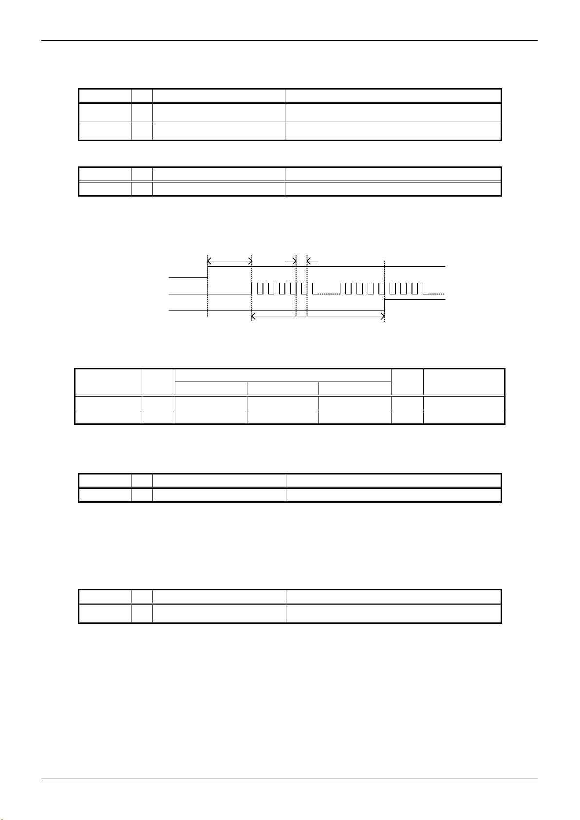
Signal name I/O Function Remarks
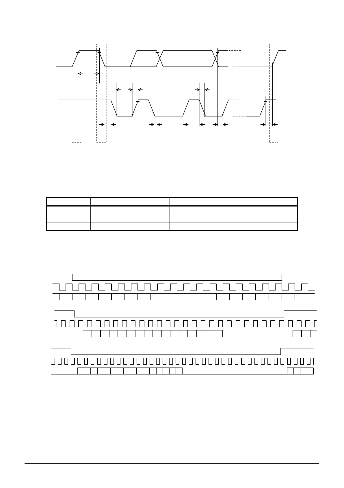
RESETX I System reset input terminal
To disable a reset signal, continue L input for more than 5 us after all of the supply voltage reach the specified value and
clock input from the oscillation I/O terminal becomes stable. (See Figure V.1.)
Power
supply
XIN_PLL
RESETX
’tal (16.9344 MHz) connection
input terminal
’tal (16.9344 MHz) connection
terminal
Oscillation stabilization
standby time
Technical Note
clk
f
Clock frequency
Reset L interval
V.2 SEL_SLAVE
MODE1/MODE2, 3 selection input signal
Signal name I/O Function Remarks
SEL_SLAVE I Selects MODE1 or MODE2, 3. H: MODE1, L: MODE2, 3
V.3 SEL_MP3
Signal name I/O Function Remarks
SEL_MP3 I MPEG Audio Layer selection
tRSTX
Figure V.1 Reset Timing
Specification
Item Symbol
f
CLK
t
RSTX
min typ max
16.9302 16.9344 16.9386 MHz
5 - - us
Unit Remarks
SEL_SLAVE selects MODE1 (STAND ALONE MODE) or MODE 2/3 (SLAVE MODE).
By selecting SEL_SLAVE, SLAVE mode terminal setting shown in Table II.2 is enabled.
SEL_SLAVE is set only at power ON. Note that change of selection after power ON is ignored.
MPEG Audio Layer 1, 2, 3 play selection signal
H: Can play MP3 only. L: Can play MP1, MP2 and
MP3.
SEL_MP3 allows you to select the layer of the MPEG audio to be played. When enabling all the files having mp1,
mp2 or mp3 as the file extension to be played, enter L. When enabling mp3 only, enter H.
SEL_MP3 is set only at power ON. Note that change of election after power ON is ignored.
www.rohm.com
8/57
© 2012 ROHM Co., Ltd. All rights reserved.
2012.04 - Rev.
BU94604BKV
A
F
F
F
F
F
p
V.4 SEL_DOUT
Audio output selection signal
Signal name I/O Function Remarks
SEL_DOUT I Audio output selection H: Line output, L: I2S 3 lines serial output/SPDIF
This SEL_DOUT selects audio output signal.
Table V4.1 “Audio output” shows the audio outputs for each MODE.
Also table V4.2 ”I2S_fs” shows the I2S output formats for each MODE.
For command, see Chapter VI.
"TEST terminal" needs to be pull-up to 3.3V power supply.
Technical Note
TableV.4.1 Audio output
Pin No.
44 Line Out Rch O OF
46 Line Out Lch O OF
53 LED_ACCESS O OF
54 LED_RANDOM O OF
55 LED_REPEAT O OF
V.5 SEL_VOL
MODE1 MODE2,3
SEL_DOUT=H SEL_DOUT=L SEL_DOUT=H
function I/O PU function I/O PU function I/O PU function I/O PU function I/O PU
HiZ O OFFLine Out Rch O OFF HiZ O OFF HiZ O OFF
HiZ O OFFLine Out Lch O OFF HiZ O OFF HiZ O OFF
I2S LR CLOCK O OFFTEST terminal I ON I2S LR CLOCK O OFF SPDIF O OFF
I2S BIT CLOCK O OFFTEST terminal I ON I2S BIT CLOCK O OFF TEST terminal I OFF
I2S LRDATA O OFFTEST terminal I ON I2S LRDATA O OFF TEST terminal I OFF
SEL_DOUT=L
I2S SPDIF ON
Table V.4.2 I2S_fs
MODE1 32fs
MODE2/3 Can select 32fs, 48fs, 64fs by command.
SEL_DOUT is set only at power ON. Note that change of selection after power ON is ignored.
Sound volume operation selection signal
Signal name I/O Function Remarks
SEL_VOL I Sound volume operation
H: Sound volume operation enabled, L: Sound volume
operation disabled
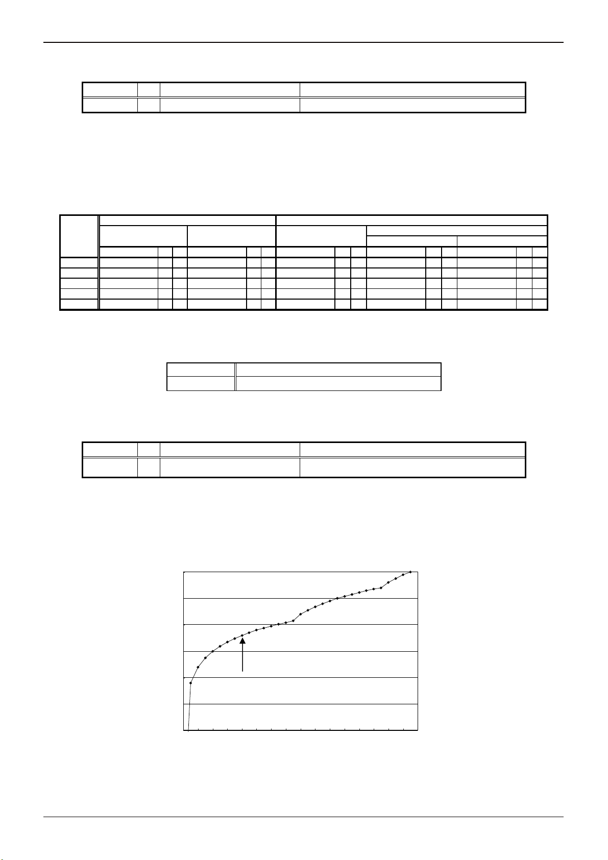
SEL_VOL selects whether sound volume operation is to be enabled or disabled.
Sound volume operation is enabled when SEL_VOL=H.
Initial value of audio output is -24.1dB at power ON.
Sound volume operation is disabled when SEL_VOL=L. Audio output is fixed to 0dB.
Figure V.5 shows the relationship between audio output and sound volume step.
SEL_VOL is set only at power ON. Note that change of selection after power ON is ignored.
0
*PU・・・Pull-Up
-10
-20
-30
-40
-50
-
Audio output (dB)
-60
Initial value: -24.1 dB
(when SEL_VOL=H)
02468101214161820222426283032
Volume ste
Figure V.5 Volume Step Function
www.rohm.com
9/57
© 2012 ROHM Co., Ltd. All rights reserved.
2012.04 - Rev.

BU94604BKV
A
V.6 SEL_APLAY
Auto play selection signal at power ON/device recognition
Signal name I/O Function Remarks
SEL_APLAY I
SEL_APLAY selects whether the audio data in the memory is to be automatically played when a memory device
(USB memory or SD card) is inserted at power ON or when the system recognizes the memory device inserted.
SEL_APLAY can be selected only in MODE1. Since selection of SEL_APLAY is ignored in MODE2/3, select it
from Pull-up. When MODE2/3 is selected, audio data is halted after the system recognizes a device.
V.7 SEL_UTPKT
USB test packet
Signal name I/O Function Remarks
SEL_UTPKT I USB test packet send H: Disabled, L: USB test packet send
A test packet signal is output from USB_DP terminal or USB_DM terminal when L is set to SEL_UTPKT at power
ON.
Once enabled, SEL_UTPK keeps that state regardless of operation modes and sends out a test packet.
A test packet signal is continuously output until power turns OFF. Use SEL_UTPKT when evaluating the USB
terminal. In other cases, use it from Pull-up.
V.8 Audio output
Audio output
Signal name I/O Function Remarks
LDACO O Lch audio line output -
RDACO O Rch audio line output -
These signals are decoded MP3 music audio data line outputs.
They turn ON when the line output is selected by SEL_DOUT terminal.
V.9 MUTE control output
Audio MUTE
Signal name I/O Function Remarks
AMUTE O Audio mute control terminal H: At audio output, L: At mute
This is a control terminal to mute audio output at power ON or FF/FB (silence).
This terminal outputs H at audio output and L at mute.
Figure Ⅴ.9 shows the operation waveform.
Auto play selection signal at
device recognition
Technical Note
H: Stop after recognizing device, H: Play after
recognizing device
Figure V.9 Waveform at Audio Mute
www.rohm.com
10/57
© 2012 ROHM Co., Ltd. All rights reserved.
2012.04 - Rev.

BU94604BKV
A
V.10 KEY input format
3x4 matrix command input
Signal name I/O Function Remarks
KEY_ROW1 I
KEY_ROW2 I -
KEY_ROW3 I -
KEY_ROW4 I -
KEY_COL1 O -
KEY_COL2 O -
KEY_COL3 O -
Configure a circuit for the matrix signals terminals for KEY commands as shown in the applied circuit diagram
V.10.
The operation corresponding to the key pressed over the circuit is performed.
Details of each operation are explained in Chapter VI.2.
Technical Note
-
KEY matrix I/O signal
REPEAT RANDOM CHG_DEV+10
VOL+ FOL- FOL+VOL-
V.11 I2C interface format
I2C serial interface
Signal name I/O Function Remarks
SCL I I2C interface clock input -
SDA I/O I2C interface data I/O -
A0 I Slave address selection terminal Slave address [0] bit setting terminal
A1 I Slave address selection terminal Slave address [1] bit setting terminal
This is an I2C serial interface terminal. By inputting L to SEL_SLAVE terminal, the interface terminal becomes
enabled.
The terminal supports slave I2C operation.
V.11.1 I2C protocol
When I2C bus is in IDLE, SDA and SCL are set to H by the external Pull-up resistance. When starting
communications, the master sets SDA to L while SCL is set to H (Start condition). When ending communications,
the master sets SDA to H while SCL is set to H (Stop condition). During transfer, SDA is changed only when SCL
is set to L. Figure V.11.1 shows Start condition, Stop condition of I2C.
KEY_
ROW1
KEY_
ROW2
PLAY/
PAUSE
STOP
KEY_
ROW3
KEY_
ROW4
FFFB
KEY_
COL1
Figure V.10 KEY Matrix Applied Circuit Diagram
KEY_
COL2
KEY_
COL3
SCL
SDA
Start or
Repeated start
condition
12
MSB
8
LSB ACK
9 1
ACK
9
Stop or
Repeated start
condition
Figure V.11.1 I2C start, stop condition
www.rohm.com
11/57
© 2012 ROHM Co., Ltd. All rights reserved.
2012.04 - Rev.
BU94604BKV
A
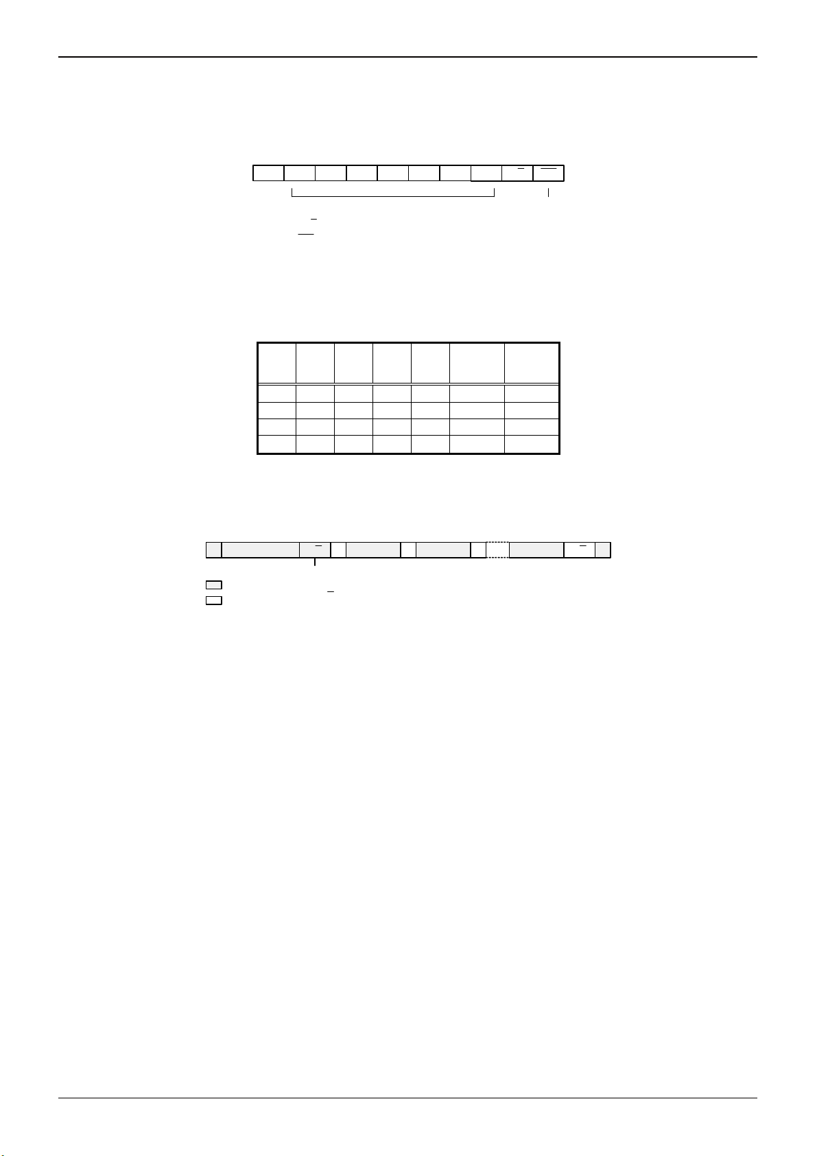
V.11.2 Slave address
An I2C bus slave address corresponds to the 7-bit addressing mode. As shown in Table V.11.2, you can select
the slave address using input of A0 terminal and A1 terminal. Figure V.11.2 shows the slave address transfer
format.
S A6 A5 A4 A3 A2 A1 A0 R/W ACK
Start
condition
R / W = Read / Write Pulse
ACK = Acknowledge
Slave Address
Figure V.11.2 Slave Address Transfer Format
Table V.11.2 Settable Slave Addresses
sent by
slave
Technical Note
MSB
A6
A5 A4 A3 A2
A1
terminal
LSB
A0
terminal
1 0 0 0 0 0 0
1 0 0 0 0 0 1
1 0 0 0 0 1 0
1 0 0 0 0 1 1
V.11.3 Write protocol from master
To send a master command using an I2C bus, follow the transfer protocol shown in Figure V.11.3. For details on
each command, see Chapter VI.
S Slave Address A Data(8bit)R/W A Data(8bit) A Data(8bit) PA/A
"0"(write)
From Master to Slave
From Slave to Master
A = Acknowledge(SDA low)
A = No Acknowledge(SDA high)
S = Start Condition
P = Stop condition
Figure V.11.3 Command send protocol
V.11.4 Read protocol to master
To send reception data using an I2C bus from the slave to the master, follow the transfer protocol shown in Figure
V.11.4.1. First, transfer the status read command (step1). Then, input SCL clock of required bytes in step 2 to
read the status.
When the device is BUSY at reception of device status or memory data, the I2C bus may possibly be occupied by
the device during BUSY. This LSI transfers the bus to the master so as not to generate such bus occupation.
However, as a BUSY state still exists inside of the system, appropriate data may not be transferred during BUSY.
Therefore, the first byte of transfer data (Step2) is used to judge the transfer data is enabled/disabled. When
specifying addresses from the master to the slave and the first byte of the transfer data immediately after data
transfer is required is 0x00, transfer data from the slave is enabled. If the first byte is 0xFF, it shows the BUSY
state. Therefore, the transfer data should be disabled. If this happens, retry command transfer at Step 1 to read
out the status.
Figure V.11.4.2 shows the relationship between the transfer data and BUSY.
* For further information on BUSY, see Chapter V.17.
www.rohm.com
12/57
© 2012 ROHM Co., Ltd. All rights reserved.
2012.04 - Rev.

BU94604BKV
A
I2C
Step1
S Slave Address A Data(8bit)R/W A Data(8bit) PA/A
Step2
S Slave Address A Data(8bit)R/W A Data(8bit) PA/A
From Master to Slave
From Slave to Master
"0"(write)
"1"(read)
A = Acknowledge(SDA low)
A = No Acknowledge(SDA high)
S = Start Condition
P = Stop condition
Figure V.11.4.1 Status Reception Protocol
Step1 command S Slave Address A 0xFF A Data(8bit) PA/AData(8bit) AR
Technical Note
Data(8bit) A
BUSY
Step1 command S Slave Address A 0x00 A Data(8bit) PA/AData(8bit) AR
Dummy byte for Busy
Dummy byte for Busy
Figure V.11.4.2 Relationship between Transfer Data and BUSY
V.11.5 I2C Bus line electrical specification and timing
SDA and SCL bus-line characteristic (Unless specified, Ta=25℃, Vcc=3.3V)
Parameter Code Min. Max. Unit
1 SDA, SCL H input voltage VIH VDD*0.7 VDD V
2 SDA, SCL L input voltage VIL DVSS VDD*0.3 V
3 SDA H output voltage VOH VDD-0.4 VDD V
4 SDA L output voltage VOL 0 0.4 V
5 SCL clock frequency fSCL 0 400 kHz
Bus-free-time between "Stop" condition and
6
"Start" condition
Hold time for "Start" condition
7
After this, the first clock pulse is generated.
tBUF 1.3 - us
tHD;STA 0.6 - us
8 LOW status hold-time of SCL clock tLOW 1.3 - us
9 HIGH status hold-time of SCL clock tHIGH 0.6 - us
10 Data-hold-time tHD;DAT 0* - us
11 Date-setup-time tSU;DAT 100 - ns
12 Rising time of SDA and SCL signal tR 20+0.1*Cb 300 ns
13 Fall time of SDA and SCL signal tF 20+0.1*Cb 300 ns
14 Setup time of "Stop" condition tSU;STO 0.6 - us
15 Capacitive load of each bus-line Cb - 400 pF
The above-mentioned numerical values are all the values corresponding to V
*To exceed an undefined area on falling edged of SCL, transmission device should internally offer the hold-time of 300ns or more for SDA signal (V
signal).
Because the "Repeated Start" condition to send "Start" condition without sending "Stop" condition doesn't correspond, after sending "Start" condition, always
send "Stop" condition.
Neither terminal SCL nor terminal SDA correspond to 5V tolerant.
IH min
and V
IL max
level.
IH min
of SCL
www.rohm.com
13/57
© 2012 ROHM Co., Ltd. All rights reserved.
2012.04 - Rev.
BU94604BKV
A
SDA
t
BUF
SCL
t
LOW
t
R
t
HD;STA
SP
t
HD;DAT
t
HIGH
Figure V.11.5 Timing chart
V.12 I2S format
I2S serial audio interface
Signal name I/O Function Remarks
LRCK O I2S Bit clock output (fs=44.1kHz) -
BCK O I2S Bit clock output -
DATA O I2S data output -
This is a serial audio interface terminal. By inputting L to SEL_DOUT terminal, the interface terminal becomes
enabled. When selecting the I2S serial audio output, the output format varies depending on MODE. *See
Chapter Ⅴ.4. MODE2 allows you to select 32fs, 48fs or 64fs. *See Chapter V.4.
Figures V.12.1. V12.2 and V.12.3 show the I2S format to be output.
t
F
t
SU;DAT
t
SU;STO
Technical Note
P
LRCK
BCK(32fs)
DATA
Left Channel
0 15 14 13 12 11 10 9 8 7 6 5 4 3 2 11 0
Right Channel
15
Figure V.12.1 I2S Output Timing (32fs)
LRCK Left Channel Right Channel
BCK(48fs)
DATA
15 14 12 11 10 9 8 7 6 5 4 3 2 1 0 15 1413
Figure V.12.2 I2S Output Timing (48fs)
LRCK
BCK(64fs)
DATA
13 1215 14 11 8 710 9 6 3 25 4 1 0 13 1215 14
Left Channel Right Channel
Figure V.12.3 I2S Output Timing (64fs)
www.rohm.com
14/57
© 2012 ROHM Co., Ltd. All rights reserved.
2012.04 - Rev.

BU94604BKV
A
V.13 SPDIF format
Digital audio interface
Signal name I/O Function Remarks
SPDIF O Digital audio output -
SPDIF output becomes enabled by setting SEL_DOUT terminal to L and setting this condition using the I2C
command. *See Chapter V.4.
Figure V.13 shows the digital audio signal output format.
Source code
Synchronous
preamble
Source code(4-31)
SPDIF output
Technical Note
034 1112 2728293031
Synchronous
preamble
Synchronous
preamble
0 0 0 0 0 0 0 0 1 0 1 1 0 1
all 0 Audio data(16bit)
(B pattern)
(M pattern)
(W pattern)
LSB MSB
Figure V.13 SPDIF Output Format
V U C P
A sub-frame of SPDIF is composed of synchronous preamble, 16-bit audio data, V bit (validity flag), U bit (user
data), C bit (channel status) and P bit (parity bit).
Output rate is fixed to 1X speed.
SPDIF outputs synchronous preamble (source code 0-3) as it is and others (source code 4-31) as bi-phase output.
It outputs L while the operation is stopped.
Synchronous preamble and C bit use 32 frames (≈4.4ms) as one cycle. Table V.13.1 and Table V.13.2 show
these formats. V bit is fixed to L. U bit uses 98 frames (≈13.3ms) as one cycle.
Table V.13.1 Synchronous Preamble Pattern
L0 R0 L1 R1 L2 R2 L3 R3 L4 R4 L5 R5
0 B W M W M W M W M W M W
1 M W M W M W M W M W M W
: : : : : : : : : : : : :
31 M W M W M W M W M W M W
Table V.13.2 C Bit Format
L0 R0 L1 R1 L2 R2 L3 R3 L4 R4 L5 R5
0 0 0 0 0 0 0
1 0 0 1 0 0 0
2 0 0 0 0 0 0
3 0 0 1 0 0 1 0 0
4 0 0 0 0 0 0
5 0 0 0 0 0 0
: : : : : : :
31 0 0 0 0 0 0
www.rohm.com
15/57
© 2012 ROHM Co., Ltd. All rights reserved.
2012.04 - Rev.

BU94604BKV
A
P bit is set to 1 if the number of “1s” of source codes 4-30 is odd, and set to 0 if the number is even. Therefore,
the number of source codes which turn to 1 for one data must be an odd value, SPDIF ends with L output and
preamble output always starts in the same direction.
V.14 USB I/F
USB I/O I/F
Signal name I/O Function Remarks
USB_DP I/O USB D+I/O terminal -
USB_DM I/O USB D-I/O terminal -
REXTI O
Differential signals of USB_DP and USB_DM enable communications with USB devices.
REXTI terminals become bias resistance connection terminals of the USB-PHY block.
V.15 SD I/F
SPI interface for SD memory card I/F
Signal name I/O Function Remarks
SD_CS O SPI chip select -
SD_CLK O SPI clock -
SD_DI O SPI data input -
SD_DO I SPI data output -
SD_CON I
These I/F enable communication with SD memory cards through SD memory card slots.
Since SD memory card slot requires detecting insertion of SD memory card, use of slot equipped with SD memory
card detecting terminal and connection to SD_CON terminal are required.
SD_CON terminal is pulled up within the device and detects SD memory card connection by L input.
V.16 MCHNG
Playing sound tune number detection output
Signal name I/O Function Remarks
MCHNG O
This signal outputs change of file to be played during playing MP3 file in the memory device.
MCHNG correctly outputs "H" during MP3 decode sequence, outputs "L" during "STOP" status.
V.17 BUSY
BUSY state detection output
Signal name I/O Function Remarks
BUSY O
This signal outputs to indicate that this LSI is in BUSY.
BUSY signal analyzes commands from the master and outputs H until the operation is executed.
This LSI ignores command input during BUSY. However, only the ABORT and STOP commands can be
accepted even during BUSY, which can be executed. *See Chapter V.11.
Technical Note
Table V.13.3 U Bit Format
L0 R0 L1 R1 L2 R2 L3 R3 L4 R4 L5 R5
0 0 0 0 0 0 0 0 0 0 0 0 0
1 0 0 0 0 0 0 0 0 0 0 0 0
2 1 0 0 0 0 0 0 0 0 0 0 0
3 1 0 0 0 0 0 0 0 0 0 0 0
: : : : : : : : : : : : :
97 1 0 0 0 0 0 0 0 0 0 0 0
USB bias resistance connection
terminal
SD card connect detection
terminal
Music tune number change
detection output signal
BUSY state detection output
signal
Connect resistance of 12kΩ 1% to GND.
H: Not detecting SD card connection.
L: Detecting SD card connection.
H: Playing, L: Tune completed/stopped
H: Busy, L: Not Busy
www.rohm.com
16/57
© 2012 ROHM Co., Ltd. All rights reserved.
2012.04 - Rev.
BU94604BKV
A
V.18 IRPTO
CONFIG outputs it for two more device connection state detection.
Signal name I/O Function Remarks
IRPTO O
When the USB device is chosen, output it to show that the USB device that two USB CONFIGURATION
DESCRIPTOR or more has in this LSI is connected. The timing of an output is dependent on the connected USB
device.
V.19 TEST terminal
By the terminal setting of TEST15, TEST16 and TEST17, It is possible to following function.
TEST15 TEST16 TEST17 Function
H H H Full function effective
L L L Only WMA and MP3 can play-back. The AAC file is disregarded.
H L L The IRPTO function is invalidated.
USB CONFIG outputs it for two
more device connection state
detection.
H: Detection , L: Undetection.
Technical Note
www.rohm.com
17/57
© 2012 ROHM Co., Ltd. All rights reserved.
2012.04 - Rev.
BU94604BKV
A
VI. Function/Operation Explanation
VI.1 File detection
VI.1.1 Function
· This function supports FAT16 and FAT32 file systems. (It does not support NTFS and FAT12.)
· The maximum number of playable files per folder
The number of files described above contains files other than AAC/WMA/MP3 and folders. If those nonAAC/WMA/MP3 files and folders exit within the folder and exceed the maximum number, all the AAC/WMA/MP3
files may not be played.
· Files less than 100 can be sorted by UNICODE in the FAT order within the folder. Files over 100 are sorted
in the FAT order. Also, the folders can be sorted in the same manner and those over 100 are sorted in the
FAT order.
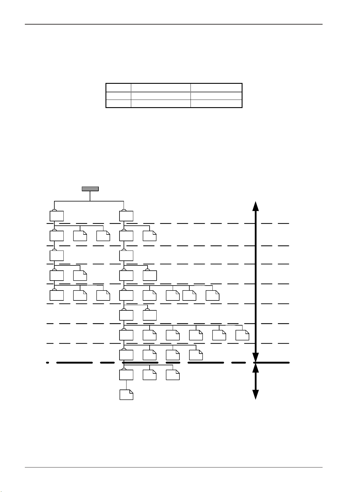
· The searchable folder hierarchy is of 8 layers containing the root folder. Figure VI.1.1 shows an example of
memory layers.
Memory
Technical Note
Table VI.1.1 Maximum Number of Playable Files
Root folder Sub folder
FAT16 512 65534
FAT32 65536 65534
USB
Folder
Folder
Folder
Folder
File File
File
File File
Playable layers
FolderFolder
Folder
Folder
Folder Folder
Folder
Folder Folder
Folder File File File File File
Folder File File File
Folder
File
File File File File
File File
Unplayable layers
File
Figure VI.1.1 Example of Memory Layers
www.rohm.com
18/57
© 2012 ROHM Co., Ltd. All rights reserved.
2012.04 - Rev.

BU94604BKV
A
VI.1.2 Playable file
The playable file extensions are *.M4A, *.3GP and *.MP4 for AAC files, *.WMA and *.ASF for WMA files, *.MP3,
*.MP2 and *.MP1 for MP3 files. (Upper case letters and lower case letters are not distinguished.) Note that
the file operation differs in the following cases:
(1) SEL_MP3: See SEL_MP3 for details.
(2) Attribute: A AAC/WMA/MP3 file whose attribute is masked can be played. A file with system attributes
(3) Data destroyed file: When the data section of AAC/WMA/MP3 file is destroyed, the music data of the file
(4) File name: A file name and its size do not depend on playing.
(5) Extension: When file data is configured in the non-AAC format and its file extension is *.M4A, *.3GP and
(6) File size: When file size is “0”, the file do not recognize at AAC/WMA/MP3 files.
(7) This LSI corresponds to the AAC file encoded by iTunes. The versions of iTunes checked operation are 4.*,
(8) When the extension of WMA file is *.ASF, this LSI corresponds to the ASF file of only an audio stream.
VI.1.3 Playing sequence
The playing sequence of AAC/WMA/MP3 files is determined based on the following rules. See Figure VI.1.3.
(1) Folders are sorted in the order written in FAT (in the order of FAT), and files 1 to 100 are sorted in the order
(2) When AAC/WMA/MP3 file exists in the root folder (the highest layer), the AAC/WMA/MP3 file is played first.
(3) When all the AAC/WMA/MP3 files in the root folder have been played, those in the folder under the root
(4) When a folder is layered under that, AAC/WMA/MP3 files in the folder are played. When not, the master
(5) After playing all the files, the master returns to the root folder as described in (2) and start playing with the
VI.1.4 Folder/file sort
Folders and files are sorted in the following sequence using this LSI.
(1) Obtain up to 100 files and 100 folders in the order written to FAT.
(2) Compare the obtained folder/file names up to 14 characters (including filename extensions) and sort them
(3) When the same strings are generated, follow the order written to FAT. When the same strings are
(4) For 101 or more folders and files, follow the order written to FAT.
* The processing of the file name and the folder name is shown in the following.
2-a) When character-code that appears first is ≧0x80 ,It’s treated as the first byte of two byte character.
Technical Note
cannot be played.
can be played as much as possible rather than disabling to play the entire file. The section which cannot
be played is muted. However, AMUTE terminal remains the H output level. When the header section of
WMA and AAC file is destroyed, it plays next.
*.MP4 the state is play next. When file data is configured in the non-WMA format and its file extension is
*.WMA, or *.ASF, the state is play next. When file data is configured in the non-MP3 format and its file
extension is *.MP3, *.MP2 or *.MP1, the state is silent playing basically. If playable data can be read, only a
part of the file can be played. The information on time required to output serial status also becomes
uncertain. Then, partial output is done but the correct time information is not output.
5.*, 6.*, and 7.0 to 7.5. The AAC file encoded with other software may cause fault, such as being in the
middle of reproduction and skipping to next.
of UNICODE. (*See Chapter VI. 1.4.) Files over 100 are sorted in the order of FAT. Folders over 100
are sorted in the same manner.
AAC/WMA/MP3 files are sorted by AAC/WMA/MP3 following SEL_MP3. Folders are sorted including null
folders and those in which AAC/WMA/MP3 files are not written. Within each folder, AAC/WMA/MP3 files
over 100 and folders over 100 are played in the order written to the FAT directory entry.
Since how to write to the directory entry depends on the OS (Operating System) processing to write to the
memory, you cannot understand the file playing sequence.
folder, if any, are played.
searches any other folders at the same layer and plays the one, if any.
first sorted file.
in the ascending order.*
generated and the extension is different, MP3 file is first, WMA file is second, and AAC file is last.
1)When the LFN(long file name) entry exists, folder/filename is processed as one character in two bytes.
2)When the LFN entry doesn't exist, the SFN(short file name) entry is processed as follows.
Byte data afterwards is treated as the second byte of two byte character-code, and treated by two
bytes as one character.
2-b) When the case that doesn't apply to 2-a) ,that is, the character-code appears first is installed within the
range of 0x00-0x7F(US-ASCII) One byte is treated as one character. '0x00' is added and enhanced to
Unicode.
Please confirm the specification of the FAT filesystem about details of LFN and SFN.
www.rohm.com
19/57
© 2012 ROHM Co., Ltd. All rights reserved.
2012.04 - Rev.

BU94604BKV
A
y
Technical Note
[Root
Folder]
E.mp3
F.mp3
G.mp3
H.mp3
J.mp3
L.mp3
M.mp3
N.mp3
O.doc
P.xls
Q.mp3
S.txt
T.txt
V.mp3
W.mp3
X.mp3
Y.mp3
Z.mp3
A.mp3
B.mp3
C.mp3
D.mp3
A_FOLDER
B_FODER
C_FOLDER
R.txt
D_FOLDER
E_FOLDER
I.mp3
K.mp3
U.mp3
Figure VI.1.3 Configurations of Folders and Files within Memory Device
Table VI.1.3 MP3 File Playing Sequence for Folder/File Configuration as in Figure VI.1.3
Playing
sequence
1 A.mp3
2 B.mp3
3 C.mp3
4 D.mp3
5 E.mp3
6 F.mp3
7 G.mp3
8 H.mp3
9 I.mp3
10 J.mp3
11 K.mp3
12 L.mp3
13 M.mp3
14 N.mp3
15 Q.mp3 · Non-MP3 files are ignored.
16 U.mp3
17 V.mp3
18 W.mp3
19 X.mp3
20 Y.mp3
21 Z.mp3
File to be
pla
ed
Remarks
· If MP3 files exist in the root folder,
those files are played first.
· Files are played in the ascending order
of UNICODE by file name.
· After all MP3 files in the root folder are
played, the master searches folders
under that layer.
· The master searches folders in the
ascending order of UNICODE by folder
name.
· After the master plays all MP3 files
including those in the lower layers
within A_FOLDER, it moves to a folder
in the same layer as A_FOLDER to
search MP3 files.
· Since there is no MP3 file in
D_FOLDER, the layers same as
A_FOLDER, the master plays MP3
files in E_FOLDER under that.
www.rohm.com
20/57
© 2012 ROHM Co., Ltd. All rights reserved.
2012.04 - Rev.

BU94604BKV
A
VI.1.5 Search within multi-drive and multi-partition
If a device is a multi-drive type or multi partition type, the LSI can recognize the drive by selecting LUN (Logical Unit
Number) for the supporting FAT. (MODE2 and MODE3)
If particular LUN isn’t selected, the LSI mounts the device whose LUN detected first. (default)
When the multi-card reader is connected, the LSI can recognize device which connected to the card-reader by
selecting LUN. But after the device is mounted, it’s impossible to recognize states whether the device connected to
the card-reader is inserted or removed.
VI.1.6 External HUB search
When the USB connector is connected to a HUB, and a FAT-supported drive is connected ahead of the HUB at
mounting the USB for this LSI, only one drive is recognized.
The LSI does not support external HUBs, it cannot detect plugging/unplugging of the drive ahead of the HUB after
the USB is mounted.
VI.2 MODE1
VI.2.1 KEY command operation
VI.2.1.1 KEY SCAN (Single Mode)
Technical Note
KEY SCAN operates in the following sequence on the circuit configuration as shown in Figure V.10 .
(1) KEY_COL1 to 3 output waveforms at timing as shown in Figure VI.2.1.
(2) By pressing KEY switch, KEY_ROW 1 to 4 are set to L at timing when KEY_COL 1 to 3 are L.
(3) When detecting L input from KEY_ROW 1 to 4 three times, the master judges that KEY has been
pressed. Then, the master starts the KEY operation.
figure VI.2.1 KEY SCAN Waveform.
KEY_COL1
KEY_COL2
KEY_COL3
PLAY
KEY_ROW1
KEY_ROW2
KEY_ROW3
KEY_ROW4
KEY_COL1
420ns
420ns
420ns
20ms
Figure VI.2.2 Operating Waveforms when KEY is Pressed
20ms 20ms 20ms 20ms 20ms 20ms
Determine that KEY is pressed
Start the operation of the pressed KEY.
www.rohm.com
21/57
© 2012 ROHM Co., Ltd. All rights reserved.
2012.04 - Rev.

BU94604BKV
A
VI.2.1.2 KEY SCAN (Hold Mode)
KEY SCAN operates in the following sequence on the circuit configuration as shown in Figure V.10 .
(1) KEY_COL1 to 3 output waveforms at timing as shown in Figure VI.2.1.
(2) By pressing KEY switch, KEY_ROW 1 to 4 are set to L at timing when KEY_COL 1 to 3 are L.
(3) When detecting L input from KEY_ROW 1 to 4 three times, the master judges that KEY has been
pressed. Then, the master starts judging status of held KEY.
(4) When pressed KEY’s decision (L input from KEY_ROW 1 to 4 three times) is detected consecutive 15
times, the master judges that KEY Mode is Hold Mode.
(5) When KEY release is detected in judging status of hold KEY, the master judges that KEY Mode is
Single Mode. Then, the master starts the KEY operation.
(6) When Hold Mode is detected, the master starts the KEY operation in Hold Mode. When KEY release is
detected in Hold Mode, the master finish the KEY operation.
The keys corresponding to Hold Mode are FF, FB, VOL+, and VOL-.
Figure VI.2.3 KEY SCAN Waveform.
Note 1: Based on the above sequence, the master determines that KEY is pressed and starts the operation of the pressed
KEY, pressing multiple KEYs at the same time will produce different operations depending on the KEY
combinations. Therefore, you cannot regulate the operation sequence correctly even simultaneously pressing
multiple KEYs will not cause any problems. In Hold Mode, Other pressed KEY is disregarded.
Note 2: Because the KEY input does not have a buffering function, KEY inputs other than those described below are
ignored.
Technical Note
www.rohm.com
22/57
© 2012 ROHM Co., Ltd. All rights reserved.
2012.04 - Rev.

BU94604BKV
A
VI.2.1.3 KEY operation
Table VI.2.1.2.1 shows the types and operations of KEYs.
Table VI.2.1.2.2 shows enabled/disabled states of KEY operations.
Table VI.2.1.2.1 KEY Commands and Operation Description
KEY COMMAND OPERATION DESCRIPTION
· When receiving “PLAY/PAUSE” key during stop, the master starts playing the first MP3 file
sorted to the recognized device.
PLAY/PAUSE
STOP
FF
FB
FOL+
FOL-
+10
VOL+/VOL-
· When receiving “PLAY/PAUSE” key during play, the master stops playing the MP3 file
temporarily. When receiving PLAY/PAUSE key again, the master restarts playing the file.
· When receiving “STOP” key during play, pause or file search, the master stops playing,
pausing or searching the MP3 file.
· When receiving “FF” KEY (Single Mode) during play or pause, the master searches the next
AAC/WMA/MP3 file in the order of sort of files being played or paused. Upon completion of
searching, the master starts playing the file.
· During play of the last file, the master returns to the first file in the order of sort and plays the
file.
· When receiving “FF” KEY (Hold Mode) during play or pause, the master starts fast forward
playing the file. When "FF" KEY release is detected, the master return to normal playing.
· When music finishes into "FF" KEY (Hold Mode), the master starts fast forward playing from
top of the next file. However, when selecting “REPEAT” or “RANDOM”, master search next
file by setup.
· When receiving “FB” KEY (Single Mode) during play or pause, the master searches the
previous AAC/WMA/MP3 file in the order of sort of files being played or paused. Upon
completion of searching, the master starts playing the file.
· During play of the first file, the master plays the last file in the order of sort.
· When receiving "FB" KEY within 1sec from top of file playing, the master searches the
previous AAC/WMA/MP3 file in the order of sort of files being played. Upon completion of
searching, the master starts playing the file. When receiving "FB" KEY over 1sec from top of
file playing, the master starts playing from top of this AAC/WMA/MP3 file.
· When receiving “FB” KEY (Hold Mode) during play or pause, the master starts fast backward
playing the file. When "FB" KEY release is detected, the master return to normal playing.
· When music finishes into "FB" KEY (Hold Mode), the master starts fast backward playing
from end of the previous file. However, when selecting “REPEAT” or “RANDOM”, master
search previous file by setup.
· When receiving “FOL+” KEY during play or pause, the master searches the AAC/WMA/MP3
files in the next folder in the order of sort of the folder in which the file being played or paused
exists. Upon completion of search, the master plays the file.
· During play of the file in the last folder in the order of sort, the master plays the first file in the
order of sort.
· When receiving “FOL-“ KEY during play or pause, the master searches the AAC/WMA/MP3
files in the next folder in the order of sort of the folder in which the file being played or paused
exists. Upon completion of search, the master plays the file.
· During play of the file in the first folder in the order of sort, the master plays the first file in the
order of sort in the last folder.
· When receiving “+10” KEY during play or pause, the master searches AAC/WMA/MP3 files
10 files next to the current one in the order of sort of the file being played or paused. Upon
completion of search, the master starts playing the file.
· When the remaining files are less than 10 during play of the current file, the master plays the
first file.
· When receiving “VOL+/VOL-“ KEY while SEL_VOL terminal is set to H, the master controls
sound volume.
· Sound volume can be controlled at 32 steps from -∞ (minimum volume) to 0dB (maximum
volume).
· Since VOL+/VOL- KEY does not judge release of KEY, the master turns up or down volume
step by step when determining press of the KEY. Therefore, VOL KEY can be held down.
Technical Note
www.rohm.com
23/57
© 2012 ROHM Co., Ltd. All rights reserved.
2012.04 - Rev.

BU94604BKV
A
(
CHNG_DEV
REPEAT
RANDOM
Technical Note
· The master selects the device between USB memory and SD memory card. To do this,
both devices should be connected or one device should correspond to the other (USB to SD
or SD to USB). Otherwise, this key operation is ignored.
· Stop after selecting the device at the top tune of the device.
· REPEAT and RANDOM settings return to the initial values.
· When inserting both USB Memory and SD Memory card, or neither USB Memory nor SD
Memory card, the master precedes USB Memory.
· This key changes the mode of repeat.
· Press of “REPEAT” KEY toggles like: “repeat all tunes in memory” “repeat one tune”
“repeat within folder”.
· When selecting “repeat within folder”, the master repeats AAC/WMA/MP3 files within the
folder being played. The initial setting is “repeat all tunes in memory”.
· This key plays the range of 128 files from the current one being played in the order of sort
at random.
· “RANDOM” KEY is enabled to change mode only during play, pause or stop.
Table VI.2.1.2.2 KEY Operation Enabled/Disabled
After recognizing device
PLAY/
PAUSE
STOP
FF
FB
FOLDER+
FOLDER-
VOL+
VOL-
+10
CHNG_DEV
REPEAT
RANDOM
= Enabled = Disabled
VI.2.2 LED operation
Seven types of LEDs used to display the LSI operation states are controlled. Table VI.2.2 shows the types and
states of LEDs.
Search or pause)
Recognize
either USB
or SD
Recognize
both USB
and SD
Table VI.2.2 Types of LEDs and operation description
During play of device
Recognize
either USB
or SD
Recognize
both USB
and SD
Searching
Recognize
either USB
or SD
Error
Recognize
both USB
and SD
Types of LEDs Operation description
Lights when an error occurs. This happens in the following cases:
LED_ERROR
LED_PLAY Lights during play. Blinks during pause.
LED_PSD
LED_PUSB
LED_ACCESS Lights during access to USB memory or SD memory card.
LED_RANDOM Lights during random play.
LED_REPEAT
www.rohm.com
24/57
© 2012 ROHM Co., Ltd. All rights reserved.
(1) Neither USB memory nor SD memory card is connected. No AAC/WMA/MP3 file
exists even if these devices are connected.
(2) Communication error or disconnection occurs in the memory being played.
Lights when SD memory card is connected and played.
Blinks when SD memory card is connected but SD memory card is not selected.
Goes off when SD memory card is not connected.
Lights when USB memory is connected and played.
Blinks when USB memory is connected but USB memory card is not selected.
Goes off when USB memory is not connected.
Lights during folder repeat. Blinks during repeat of one tune. Goes off during repeat
all tunes in memory
2012.04 - Rev.

BU94604BKV
A
VI.3 MODE2
VI.3.1 Command operation
You can operate commands via the I2C serial interface. When using the LSI in MODE2, it can be operated by setting
SEL_SLAVE to L. The length of command to be sent varies depending on which command is selected.
Table VI.3.1.1 shows the command specifications.
Table VI.3.1.2 shows enabled/disabled state of each command.
Technical Note
Table VI.3.1.1 Command Operation Description
Command name
PLAY
PAUSE 0x02 - -
STOP 0x03 - -
VOL+ 0x04 - -
VOL- 0x05 - -
REPEAT 0x06 - -
RANDOM 0x07 - -
CHNG_DEV 0x08 - -
ABORT 0x0C - -
Command
byte length
2 0x50
1st 2nd 3rd 4th~
Command Operation description
· When receiving “PLAY” command during stop, the master starts playing
the AAC/WMA/MP3 file currently selected. The order sorted from the
root folder is initially set.
· When receiving “PLAY” command during pause, the master restarts
0x01 - -
playing the file from that point.
· When a state which disables MP3 decoding for more than 5 seconds
during play, status “DECO_ERR” is set to H. MP3 decoding is continued.
· When receiving “PLAY” command during fast forward (or backward)
playing, the master restarts normal playing the file from current point.
· When receiving “PAUSE” command during play, the master stops playing
the AAC/WMA/MP3 files temporarily.
· When receiving “STOP” command during play, pause or file search, the
master stops playing the AAC/WMA/MP3 file.
· When receiving “STOP” command during fast forward (or backward)
playing, the master stops playing the file.
· “STOP” command can be received even during BUSY.
· When SEL_VOL is set to H, “VOL+” command is enabled.
· When receiving “VOL+” command, the master controls sound volume.
· Sound volume can be controlled at 32 steps from -∞ (minimum volume)
to 0dB (maximum volume).
· When SEL_VOL is set to H, “VOL-“command is enabled.
· When receiving “VOL-“command, the master controls sound volume.
· Sound volume can be controlled at 32 steps from -∞ (minimum volume)
to 0dB (maximum volume).
· This command selects the mode during repeat.
· REPEAT command toggles like: “repeat all tunes in memory” “repeat
one tune” “repeat within folder”.
· When STATUS RPT_OFF is set as ON by "REPRAND" command,
REPEAT command toggles like: “all play in memory” “one file play”
“play within folder”. In this mode, it stops upon completion of playing.
· When selecting “repeat within folder”, the master repeats AAC/WMA/MP3
files within the folder being played.
· The initial setting is “repeat all tunes in memory”.
· The last setting to “REPRAND”, “REPEAT” and “RANDOM” commands
will be enabled.
· This command is as same as the “REPEAT” command in MODE1.
· This key plays the range of 128 files from the current one being played
in the order of sort at random.
· When STATUS RPT_OFF is set as ON by "REPRAND" command,
REPEAT command toggles like: “one random file play” “all play with
random in memory”. In this mode, it stops upon completion of playing.
· The last setting to “REPRAND”, “REPEAT” and “RANDOM” commands
will be enabled.
· This command is as same as the “RANDOM” command in MODE1.
· The command selects the device between USB memory and SD memory
card. To do this, both devices should be connected or one device
should correspond to the other (USB to SD or SD to USB). Otherwise,
this key operation is ignored.
· Stop after selecting the device at the top tune of the device.
· REPEAT and RANDOM settings return to the initial values.
· This command interrupts Tag analysis.
· It interrupts Tag analysis only the file is being played.
www.rohm.com
25/57
© 2012 ROHM Co., Ltd. All rights reserved.
2012.04 - Rev.

BU94604BKV
A
Technical Note
SET_RESUME_
INFO1
SET_RESUME_
INFO2
SET_RESUME_
INFO3
SET_RESUME_
INFO4
SET_RESUME_
INFO5
SET_RESUME_
INFO6
SET_RESUME_
INFO7
SET_RESUME_
INFO8
FF
FF&PLAY 0x01
FFP_ON 0x02
8 0x51
4 0x55
0x41
0x42
0x43
0x44
0x45
0x46
0x47
0x48
0x01
RESUME INFO
1byte-6byte
RESUME INFO
7byte-12byte
RESUME INFO
13byte-18byte
RESUME INFO
19byte-24byte
RESUME INFO
25byte-30byte
RESUME INFO
31byte-36byte
RESUME INFO
37byte-42byte
RESUME INFO
37byte-42byte
0x00
0x00
· This command sets byte 1 to 6 of 42-byte data obtained by
“READ_RESUME_INFO”.
· This command sets byte 7 to 12 of 42-byte data obtained by
“READ_RESUME_INFO”.
· This command sets byte 13 to 18 of 42-byte data obtained by
“READ_RESUME_INFO”.
· This command sets byte 19 to 24 of 42-byte data obtained by
“READ_RESUME_INFO”.
· This command sets byte 25 to 30 of 42-byte data obtained by
“READ_RESUME_INFO”.
· This command sets byte 31 to 36 of 42-byte data obtained by
“READ_RESUME_INFO”.
· This command sets byte 37 to 42 of 42-byte data obtained by
“READ_RESUME_INFO”. When RESUME reproduction is possible, play
started that music. When RESUME is impossible, play the head music of
media is started.
· About some kind of setting of Resume Play, see “Application Note – V.2.9
Resume Play Method”.
· This command sets byte 37 to 42 of 42-byte data obtained by
“READ_RESUME_INFO”. When RESUME reproduction is possible, it
stops in the music. When RESUME is impossible, it stops at the head of
media.
· About some kind of setting of Resume Play, see “Application Note – V.2.9
Resume Play Method”.
· When receiving FF command during play, pause or stop, the master
searches the next AAC/WMA/MP3 file in the order of sort of the file being
played or paused.
· During play of the last file, the master returns to the first file in the order
of sort.
· Operation stops upon completion of search.
· When ID3 or WMA-TAG analysis is set by SEL_ID3 command, operation
stops upon completion of TAG analysis.
· When receiving ”FF&PLAY” command during play, pause or stop, the
master searches the next AAC/WMA/MP3 file in the order of sort of the
file being played or paused.
· During play of the last file, the master returns to the first file in the order
of sort.
· Operation starts playing, after completion of search.
· When TAG analysis is set by SEL_ID3 command, the master plays the
file upon completion of TAG analysis.
· When receiving FFP_ON command during play, pause or stop, the
master starts fast forward playing from current point.
When music finishes into that FFP_ON command is ON, the master
·
starts fast forward playing from top of the next file. When setting
“REPEAT” or “RANDOM”, master search next file by setup.
FFP_OFF 0x03
FB 0x02 0x00 0x00
www.rohm.com
26/57
© 2012 ROHM Co., Ltd. All rights reserved.
· When receiving FFP_OFF command during fast forward playing, the
master restarts normal playing from current point.
· When receiving “FB” command during play, pause or stop within 1sec
from top of file playing, the master searches the previous AAC/WMA/MP3
file in the order of sort of files being played or paused. When receiving
“FB” command during play or pause over 1sec from top of file playing,
the master searches top of present AAC/WMA/MP3 file.
· The master returns to the last file during play of the first file within 1sec
from top of file playing.
· Upon completion of search, the operation stops.
· When TAG analysis is set by SEL_ID3 command, operation stops upon
completion of TAG analysis.
2012.04 - Rev.

BU94604BKV
A
·· When receiving “FB&PLAY” command during play, pause or stop within
1sec from top of file playing, the master searches the previous
AAC/WMA/MP3 file in the order of sort of files being played or paused.
When receiving “FB&PLAY” command during play or pause over 1sec
from top of file playing, the master searches top of present
FB&PLAY 0x01
FBP_ON 0x02
AAC/WMA/MP3 file.
· The master returns to the last file during play of the first file within 1sec
from top of file playing.
· Operation starts playing, after completion of search.
· When TAG analysis is set by SEL_ID3 command, the master plays the
file upon completion of TAG analysis.
· When receiving FBP_ON command during play, pause or stop, the
master starts fast backward playing from current point.
·
When music finishes into that FBP_ON command is ON, the master
starts fast backward playing from end of previous file. When
setting “REPEAT” or “RANDOM”, master search previous file by
setup.
FBP_OFF 0x03
FOL+
0x03
FOL+&PLAY 0x01
FOL-
0x04
FOL-&PLAY 0x01
+10 0x05 0x00 0x00
0x00
0x00
· When receiving FBP_OFF command during fast backward playing, the
master restarts normal playing from current point.
· When receiving “FOL+” command during play, pause or stop, the master
searches the next folder in the order of sort of the folder in which the file
being played or paused exists.
· The master returns to the first folder in the order of sort during play of the
last folder.
· The operation stops upon completion of search.
· When TAG analysis is set by SEL_ID3 command, operation stops upon
completion of TAG analysis.
· When receiving “FOL+&PLAY” command during play, pause or stop, the
master searches the next folder in the order of sort of the folder in which
the file being played or paused exists.
· The master returns to the first folder in the order of sort during play of the
last folder.
· Operation starts playing, after completion of search.
· When TAG analysis is set by SEL_ID3 command, the master plays the
0x00
file upon completion of TAG analysis.
· When receiving “FOL-“ command during play, pause or stop, the master
search the next folder in the sort of the folder in which the file being
played or paused exists.
· During play of the first folder, the master returns to the last folder in the
order of sort.
· The operation stops upon completion of search.
· When TAG analysis is set by SEL_ID3 command, operation stops upon
completion of TAG analysis.
· When receiving “FOL-&PLAY“ command during play, pause or stop, the
master searches the next folder in the order of sort of the folder in which
the file being played or paused exists.
· During play of the top folder, the master returns to the first folder in the
order of sort.
· Operation starts playing, after completion of search.
· When TAG analysis is set by SEL_ID3 command, the master plays the
file upon completion of TAG analysis.
· When receiving “+10” command during play, pause or stop, the master
searches the AAC/WMA/MP3 file of the 10
the file being played or paused.
· When the remaining files to be played are less than 10 in the order of
sort, the master returns to the first file.
· The operation stops upon completion of search.
· When TAG analysis is set by SEL_ID3 command, operation stops upon
completion of TAG analysis.
Technical Note
th
tune in the order of sort of
www.rohm.com
27/57
© 2012 ROHM Co., Ltd. All rights reserved.
2012.04 - Rev.

BU94604BKV
A
Technical Note
· When receiving “+10&PLAY” command during play, pause or stop, the
master searches the AAC/WMA/MP3 file of the 10
sort of the file being played or paused.
+10&PLAY 0x01
-10
0x06
-10&PLAY 0x01
USB_MNT_R
EADY
4 0x5D 0x0B 0x01 0x00
0x00
· When the remaining files to be played are less than 10 in the order of
sort, the master returns to the first file.
· Operation starts playing, after completion of search.
· When TAG analysis is set by SEL_ID3 command, the master plays the
file upon completion of TAG analysis.
· When receiving “-10” command during play, pause or stop, the master
searches the AAC/WMA/MP3 file of the previous 10
sort of the file being played or paused.
· When playing the top 10 or less files in the order of sort, the master
returns to the first file.
· The operation stops upon completion of search.
· When ID3 or WMA-TAG analysis is set by SEL_ID3 command, operation
stops upon completion of TAG analysis.
· When receiving “-10&PLAY” command during play, pause or stop, the
master searches the AAC/WMA/MP3 file of the previous 10
order of sort of the file being played, paused or stopped.
· When playing the top 10 or less files in the order of sort, the master
returns to the first file.
· Operation starts playing, after completion of search.
· When TAG analysis is set by SEL_ID3 command, the master plays the
file upon completion of TAG analysis.
· This command prepares for USB memory mount.
· Be sure to send this command when STATUS turns to USB_INS=H and
BUSY=L..
th
tune in the order of
th
tune in the order of
th
tune in the
0x00
SET_DOUT 4 0x51 0x20
0x01 0x01
0xFF 0x00
0x00 - -
0x01 - -
0x02 - -
0x03 - -
0x04 - -
SET_EQ
* See Chapter
VI.3.3.
SET_VOL 2 0x53
2 0x52
0x05 - -
0x07 - -
0x08 - -
0x09 - -
0x0A - -
0x0B - -
0x0C - -
0x0D - -
0x0F - -
Setting
value
· This command outputs the audio data in the I2S (32fs) format.
0x58
· When SET_DOUT command is sent, SEL_DOUT terminal setting is
· This command outputs the audio data in the I2S (48fs) format.
0x59
· When SET_DOUT command is sent, SEL_DOUT terminal setting is
· This command outputs the audio data in the I2S (64fs) format.
0x5B
· When SET_DOUT command is sent, SEL_DOUT terminal setting is
· This command performs serial audio interface (SPDIF) output.
· When SET_DOUT command is sent, SEL_DOUT terminal setting is
· This command stops serial audio interface (I2S, SPDIF) output.
· When SET_DOUT command is sent, SEL_DOUT terminal setting is
This command turns OFF the EQ setting.
POPS
JAZZ
ROCK
CLASSIC
R&B
This command turns OFF the EQ setting.
BASS BOOST1
POPS+BASS BOOST1
JAZZ+BASS BOOST1
ROCK+BASS BOOST1
CLASSIC+BASS BOOST1
R&B+BASS BOOST1
BASS BOOST2
· This command sets the sound volume to the 2nd byte value of the
- -
ignored
ignored
ignored
ignored
ignored
command. The setting value ranges 32 steps from 0x00 to 0x1F.
Any value outside of the above range is ignored.
www.rohm.com
28/57
© 2012 ROHM Co., Ltd. All rights reserved.
2012.04 - Rev.

BU94604BKV
A
REPRAND 2 0x54
SEL_ID3 2 0x56
SEL_TOC 2 0x57
SEL_12MOUT 2 0x58
0x00 - -
0x01 - -
0x02 - -
0x03 - -
0x04 - -
0x05 - -
0x06 - -
0x07 - -
0x00 - -
0x01 - -
0x00 - -
0x01 - -
0x00 - -
0x01 - -
Technical Note
· This command repeats all the tunes within the memory. This is initially
set.
· The last setting to “REPRAND”, “REPEAT” and “RANDOM” commands
will be enabled.
· The command repeats playing the AAC/WMA/MP3 file within the folder
being played.
· The last setting to “REPRAND”, “REPEAT” and “RANDOM” commands
will be enabled.
· This command repeats playing the MP3 file being played.
· The last setting to “REPRAND”, “REPEAT” and “RANDOM” commands
will be enabled.
· This command plays through the range of 128 files in the order of the
sort from the current one being played at random.
· The last setting to “REPRAND”, “REPEAT” and “RANDOM” commands
will be enabled.
· This command plays all the tunes within the memory. STATUS RPT_OFF
is set as ON.
· It stops after the last file playing.
· The last setting to “REPRAND”, “REPEAT” and “RANDOM” commands
will be enabled.
· This command plays all the tunes within the folder being played. STATUS
RPT_OFF is set as ON.
· It stops after the last file playing within the folder.
· The last setting to “REPRAND”, “REPEAT” and “RANDOM” commands
will be enabled.
· This command plays one tunes. STATUS RPT_OFF is set as ON.
· It stops after the file playing.
· The last setting to “REPRAND”, “REPEAT” and “RANDOM” commands
will be enabled.
· This command plays through the range of 128 files in the order of the
sort from the current one being played at random. STATUS RPT_OFF is
set as ON.
· It stops after the file playing.
· The last setting to “REPRAND”, “REPEAT” and “RANDOM” commands
will be enabled.
· This command does not perform ID3Tag analysis written to the MP3 file.
· This command does not perform WMATag analysis written to the WMA
file.
· This command does not perform AACTag analysis written to the AAC file.
· The file played immediately after set will be enabled first.
· This command analysis ID3Tag written to the MP3 file.
· This command analysis WMATag written to the WMA file.
· This command analysis AACTag written to the AAC file.
· The file played immediately after set will be enabled first.
· Upon completion of Tag analysis, the data is written to the status register.
· This command does not perform TOC analysis.
· TOC analysis is not performed at initial setting.
· When receiving the command, inserting into the device or changing the
device, the master analyzes the total folders (including root directory) and
total AAC/WMA/MP3 files within the device.
· The number of total AAC/WMA/MP3 files conforms to SEL_MP3 terminal.
· When receiving the command, only change from OFF to ON is executed.
· Upon completion of TOC analysis, the master returns to the top tune of
the device and stops.
· After TOC analysis, the data is written to the status register.
· This command stops 12MHz clock output from CLKOUT12 terminal.
· This command enables 12 MHz clock output from CLKOUT12 terminal.
0x00 - -
SEL_WDT 2 0x5A
0x01 - -
www.rohm.com
29/57
© 2012 ROHM Co., Ltd. All rights reserved.
· This command stops WDT.
· This command writes “1” to
STATUS WDT_RFLG.
2012.04 - Rev.

BU94604BKV
A
A
A
A
A
SET_RPM 6 0x5B
SET_RPM_ATT 4 0x5B
SET_UPLOAD
_FILE1
SET_UPLOAD_
FILE2
UPLOAD_END 2 0x51 0x53 - -
SET_TOUT_M 4 0x5D 0x07 0xYY 0xXX
SET_TOUT_C 4 0x5D 0x08 0xYY 0xXX
SET_USB_R_W
AIT
GET_ VENDOR
FORCE_DISC
ON_USB
FORCE_CON
_USB
8 0x51 0x51
8 0x51 0x52
4 0x5D 0x09 0xXX 0x00
2 0x5F 0x16 - -
2 0x5D 0x02 - -
2 0x5D 0x0A - -
0x00 setting
0x01 setting 0x00
NAME[0:5]
NAME[6:7]
EXT[0:2]
Technical Note
· This command set up playtime and skiptime for fast forward playing and
fast backward playing. Fast forward and fast backward playing repeat
this cycle by making {playtime(M) + skiptime(N) +error(O)} into 1 cycle.
With an error, it depends on the cajoled error between the minimum
decoding unit and playtime, and the real time which searches skiptime.
Errors differ by every file and every composition in memory.
· This command set up that playtime is M[15:0]=[4th byte, 3rd byte] and
skiptime are N[15:0]=[6th byte and 5th byte]. Initial value set playtime is
300 mili second=M[15:0]=[4 th byte=x01, 3rd byte=x2C] and skiptime is
2100 mili second=N[15:0]=[6 th byte=x08, 5 th byte=x34].
When command set up to 0x0, setting value is initial value.
The playtime should set up 300ms or more, and skiptime should set up
below (playtime x16).
· This command set up the attenuation level under fast forward and
backward playing.
An attenuation level serves as (-6dB X [3rd byte]).
A setup can be specified from 0x00 to 0x10.As for an initial value,
0x02=-12dB is set up. It becomes equivalent to MUTE by setup of 0x10.
Specify the part of the first half of the file name of the file for File Read
Function.
*Bury it by 0x20 when the file name(NAME) doesn't come up to eight bytes.
Specify the part of the latter half of the file name of the file for File Read
Function.
*Bury it by 0x20 when the file name(NAME) doesn't come up to eight bytes.
Bury it by 0x00 when the file extension doesn't come up to three bytes.
It targets neither the file name comparison since 0x00 of the end in the
comparison.
The File Read function is ended.
Transmit after completing the file reading.
The ACK timeout of the command under memory mount is set up.
The set point x100 (msec) is timeout. At the time, XX is upper byte and YY is
lower byte.
n initial value is 30 sec (YY=0x2C, XX=0x01), and maximum value is 60
sec (YY=0x58, XX=0x02).If set point is over the maximum value, this
command is ignored.
Mount ERROR will be carried out if a timeout occur.
The ACK timeout of the commands at the time of PLAY or STOP or PAUSE
(except during mount) is set up.
The set point x100 (msec) is timeout. At the time, XX is upper byte and YY is
lower byte.
n initial value is 5 sec (YY=0x32, XX=0x00), and maximum value is 60 sec
(YY=0x58, XX=0x02). If set point is over the maximum value, this command
is ignored.
Communication ERROR will be carried out if a timeout occur.
The wait time after bus reset is set up at the time of USB memory
recognition.
The set point (XX) x200 (msec) is wait time.
n initial value is 600 msec (XX=0x03), and maximum value is 51.2 sec
(XX=0xFF).
vendor code and Product ID are stored in COMAREA.
Please read COMAREA after GET_VENDOR command transmission and
acquire code data.
Offset 0x20:Vendor code Lower byte
0x21:Vendor code Upper byte
0x22:Product code Lower byte
0x23:Product code Upper byte
Force mounted USB memory to be disconnected.
Mounts USB memory again, which Mount ERROR occurred.
www.rohm.com
30/57
© 2012 ROHM Co., Ltd. All rights reserved.
2012.04 - Rev.

BU94604BKV
A
Technical Note
FORCE_DISC
ON_SD
FORCE_CON
_SD
SET_LUN
RESET_LUN
4 0x5D 0x0C 0x01 0x00
4 0x5D 0x0C 0x00 0x00
4 0x5D 0x0D setting 0x00
2 0x5D 0x0E - -
Force SD memory to be disconnected, which Mount ERROR occurred
Mounts SD memory again, which was disconnected by
FORCE_DISCON_SD command.
LUN, which USB memory mounts, is specified.
LUN specified at the time of USB connection mounts.
When another LUN is already mounted, it re-mounts to specified LUN.
When not specifying LUN, effective LUN becomes an AUTO setup and LUN
detected first is mounted at the time of USB memory connection.
(Initial value)
Effective LUN is set to AUTO and LUN detected first comes to be mounted
at the time of USB memory connection.
www.rohm.com
31/57
© 2012 ROHM Co., Ltd. All rights reserved.
2012.04 - Rev.

BU94604BKV
A
Table VI.3.1.2 Command Enabled/Disabled in Various States
After recognizing
device, search or
PLAY ○ ○ × × × ○ ○ × ×
PAUSE × × ○ ○ × ○ ○ × ×
STOP × × ○ ○ ○ ○ ○ × ×
VOL+ ○ ○ ○ ○ × ○ ○ ○ ○
VOL- ○ ○ ○ ○ × ○ ○ ○ ○
REPEAT ○ ○ ○ ○ × ○ ○ × ×
RANDOM ○ ○ ○ ○ × ○ ○ × ×
CHNG_DEV × ○ × ○ × ○ ○ × ○
ABORT × × × × ○ × × × ×
SET_RESUME_
INFO1-8
FF ○ ○ ○ ○ × × × × ×
FF&PLAY ○ ○ ○ ○ × × × × ×
FFP_ON × × ○ ○ × ○ ○ × ×
FFP_OFF × × × × × ○ × × ×
FB ○ ○ ○ ○ × × × × ×
FB&PLAY ○ ○ ○ ○ × × × × ×
FBP_ON × × ○ ○ × ○ ○ × ×
FBP_OFF × × × × × × ○ × ×
FOL+ ○ ○ ○ ○ × × × × ×
FOL+&PLAY ○ ○ ○ ○ × × × × ×
FOL- ○ ○ ○ ○ × × × × ×
FOL-&PLAY ○ ○ ○ ○ × × × × ×
+10 ○ ○ ○ ○ × × × × ×
+10&PLAY ○ ○ ○ ○ × × × × ×
-10 ○ ○ ○ ○ × × × × ×
-10&PLAY ○ ○ ○ ○ × × × × ×
USB_MNT_READY ○ ○ ○ ○ ○ ○ ○ ○ ○
SET_DOUT ○ ○ ○ ○ × ○ ○ ○ ○
SET_EQ ○ ○ ○ ○ × ○ ○ ○ ○
SET_VOL ○ ○ ○ ○ × ○ ○ ○ ○
REPRAND ○ ○ ○ ○ × ○ ○ × ×
SEL ID3 ○ ○ ○ ○ × ○ ○ × ×
SEL_TOC ○ ○ ○ ○ × ○ ○ × ×
SEL 12MOUT ○ ○ ○ ○ × ○ ○ ○ ○
SET_WDT ○ ○ ○ ○ × ○ ○ ○ ○
SET_RPM ○ ○ ○ ○ × ○ ○ ○ ○
SET_RPM_ATT ○ ○ ○ ○ × ○ ○ ○ ○
SET_UPLOAD_FILE1
SET_UPLOAD_FILE2
UPLOAD_END
SET_TOUT_M
SET_TOUT_C
SET_USB_RWAIT
GET_VENDOR
Recognize
either USB
pause
Recognize
or SD
○ ○ ○ ○ × ○ ○ ○ ○
○ ○ ○ ○ × ○ ○ ○ ○
○ ○ ○ ○ × ○ ○ ○ ○
○ ○ ○ ○ × ○ ○ ○ ○
either USB
or SD
○ ○ ○ ○ × × × × ×
After recognizing the USB memory, only the halt condition is the command effective.
During play of device
Recognize
either USB
or SD
Recognize
both USB
and SD
Search
ing
During
FFP
During
FBP
Recognize
either USB
or SD
Technical Note
Error
Recognize
both USB
and SD
www.rohm.com
32/57
© 2012 ROHM Co., Ltd. All rights reserved.
2012.04 - Rev.

BU94604BKV
A
FORCE_DISCON_USB ○ ○ ○ ○ ○ ○ ○ × ×
FORCE_CON_USB × × × × × × × ○ ○
FORCE_DISCON_SD × × × × × × × ○ ○
FORCE_CON_SD × × × × × × × ○ ○
SET_LUN ○ ○ ○ ○ × ○ ○ ○ ○
RESET_LUN ○ ○ ○ ○ × ○ ○ ○ ○
○= Enabled = Disabled
Technical Note
www.rohm.com
33/57
© 2012 ROHM Co., Ltd. All rights reserved.
2012.04 - Rev.

BU94604BKV
A
VI.3.2 Status output
The operation information, such as internal status, play time information, folder information, file information, ID3Tag
information, AACTag information and WMATag information, is output using an I2C interface.
Statuses as shown in Table VI. 3.2.1 MODE 2 Status Register Map are output.
The status register has a ring buffer structure of OFFSET 0x00-0x7F. The OFFSET position is automatically
incremented after reading byte data.
Status read specifies OFFSET of the status register map. There are two methods available: to read a desired
number of bytes continuously from the OFFSET position and to read the data by one command without specifying the
OFFSET position. Figure VI.3.2.2 shows the status output commands. Table VI.3.2.3 shows the enabled/disabled
state of the status output commands.
Status register outputs a byte data of OFFSET 0x00-0x7F by "Little Endian" format
Technical Note
Table VI. 3.2.1 MODE2 Status Register Map
OFFSET Status
0x00 STATUS1
0x01 STATUS2
0x02 STATUS3
0x03 STATUS4
0x04 STATUS5
0x05 VOLINF
bit7
(MSB)
ERROR
0: No error
1: Error occurs
USBINS
0: USB not
connected
1: USB
connection
detected
BUSY
0: Not BUSY
1: BUSY
0 0 0 0
12MOUT
12 MHz clock
output
0: OFF
1: ON
0 0 0
bit6 bit5 bit4 bit3 bit2 bit1
SEARCH
0: Search stop
1: Searching
SDINS
0: SD not
connected
1: SD connection
detected
MCHNG
Tune number
change detection
0: Tune
ended/stopped
1: Playing/
stop before
playing
WDT_RFLG
0: after RESET
SEL_ID3
0: ID3Tag OFF
1: ID3Tag ON
USBFILE
Playable file within
USB memory
0: Absent
1: Present
0
WMAPLAY
Play file information
1: WMA , 2: AAC
3:Device with 2 configurations or more
SEL_TOC
0: TOC display
1: TOC display ON
SDFILE
Playable file within
SD memory
0: Absent
1: Present
ID3EXIST
TAG information
0: Not exist
0: MP3
OFF
1: Exist
DEC_ERR
0: No error
1: Error occurs
MDEVUSB
USB memory
recognized
1: Recognized
ID3RSID1
ID3Tag
Version1
0: Absent
1: Present
RPT_OFF
Setting after
last file playing
0: repeat
1: stop
Fast backward
playing
0: OFF
0: Not stopped
0: Not
1: Recognized
FBP
1: ON
Sound volume information
STOP
1. Stopping
MDEVSD
SD memory
0: Not
recognized
ID3RSID2
ID3Tag
Version2
0: Absent
1: Present
RANDOM
Random play
setting
0: OFF
1: ON
FFP
Fast forward
playing
0: OFF
1: ON
VOLINF
[ 4: 0 ]
PAU SE
0: Not paused
1: Pausing
PDEVUSB
PDEVUSB USB
memory
0: Stopping
1: Playing/Tag
analyzing
TINFUSB
Total number of
folders/files
within USB
memory
0: Not obtained
1: Obtained
REP1
One-tune repeat
setting
0: OFF
1: ON
0
bit0
(LSB)
Play
0: Not played
1: Playing
PDEVSD
PDEVUSB SD
memory
0: Stopping
1: Playing/Tag
analyzing
TINFSD
Total number
of folders/files
within SD
memory
0: Not
obtained
1: Obtained
REPFOL
Folder repeat
setting
0: OFF
1: ON
RES_ERR
Resume error
0: No error
1: Error
occurs
EQINF
Equalizer setting information
0000: OFF
0001: POPS
0010: JAZZ
0011: ROCK
0100: CLASSIC
0x06 EQINF
0x07 PRECOM
HUB
0x08 DOUT
www.rohm.com
34/57
© 2012 ROHM Co., Ltd. All rights reserved.
Detection Flag
0: Not Detection
1: Detection
Un Support device
Detection Flag
0: Not Detection
1: Detection
0101: R&B
1000: BASS BOOST
1001: POPS+BASS
1010: JAZZ+BASS
1011: ROCK+BASS
1100: CLASSIC+BASS
1101: R&B+BASS
1111 BASS BOOST2
Vendor code
Detection Flag
0: appleNot Detection
1: appleDetection
PRECOM
Previous Command information
0: normal
1: miss
0 0 0 0
0 0 0 0
DOUT
Audio output
0: LINE output
1: I2S / SPDIF
2012.04 - Rev.

BU94604BKV
A
0x09 DOUTINF
DOUTINF
I2S format status
0x58: 32fs(Initial value)
0x59: 48fs
0x5B: 64fs
0x00: OFF
0x01: SPDIF output
Technical Note
0x0A PFOLNL
0x0B PFOLNH
0x0C PFILENL
0x0D PFILENH
0x0E PSEC
0x0F PMIN
0x10 TFOLUSBL
0x11 TFOLUSBH
0x12 TFILEUSBLL
0x13 TFILEUSBLH
0x14 TFILEUSBHL
0x15 TFILEUSBHH
0x16 TFOLSDL
0x17 TFOLSDH
0x18 TFILESDL
0x19 TFILESDLH
0x1A TFILESDHL
0x1B TFILESDHH
Playing folder number lower-order byte
Playing folder number upper-order byte
Playing file number upper-order byte
Playing time second information
[7:4]x10 sec.
Playing time minute information
[7:4]x10 min.
USB memory total folder number lower -order byte
USB memory total folder number upper-order byte
USB memory total file number lower -order byte [15:0]
USB memory total file number upper-order byte [15:0]
USB memory total file number lower -order byte [31:16]
USB memory total file number upper-order byte [[31:16]
SD memory total folder number lower -order byte
SD memory total folder number upper-order byte
SD memory total file number lower -order byte [15:0]
SD memory total file number upper-order byte [15:0]
SD memory total file number lower -order byte [31:16]
SD memory total file number upper-order byte [31:16]
PFOLNL
[7:0]
PFOLNH
[15:8]
Playing file number lower-order byte
PFILENL
[7:0]
PFILENH
[15:8]
TFOLUSBL
[7:0]
TFOLUSBH
[15:8]
TFILEUSBLL
[7:0]
TFILEUSBLH
[15:8]
TFILEUSBHL
[23:16]
TFILEUSBHH
[31:24]
TFOLSDL
[7:0]
TFOLSDH
[15:8]
TFILESDLL
[7:0]
TFILESDLH
[15:8]
TFILESDHL
[23:16]
TFILESDHH
[31:24]
Playing time second information
[3:0]x1 sec.
Playing time minute information
[3:0]x1 min.
0x1C LANGL
0x1D LANGH
www.rohm.com
35/57
© 2012 ROHM Co., Ltd. All rights reserved.
Language code information lower -order byte [7:0]
Language code information upper -order byte [15:8]
LANGL
LANGH
2012.04 - Rev.

BU94604BKV
A
Technical Note
0x20
|
0x7F
COMAREA
The content varies depending on the status read command.
COMAREA
Data common area
www.rohm.com
36/57
© 2012 ROHM Co., Ltd. All rights reserved.
2012.04 - Rev.

BU94604BKV
A
Command name
READ_BUFF 0x5E OFFSET Optional
READ_STATUS
READ_PLAY_INFO 0x01 6
READ_VOL 0x02 1
READ_ID3_TITLE 0x04 64
READ_ID3_ARTIST 0x05 64
READ_ID3_ALBUM 0x06 64
READ_FILE_NAME 0x07 64
READ_FOLDER_NAME 0x08 64
READ_RESUME_INFO
* See Chapter VI.3.4.
READ_VERSION 0x10 1
READ_FILE_SIZE 0x11 4
READ_FILE_DATA 0x12 96
READ_LUN 0x17 1
Table VI. 3.2.2 MODE2 Status Output Commands
Command
1st byte 2nd byte
0x00 5
READ_EQ 0x03 1
0x09 42
0x5F
Status output
bytes
· The command outputs the desired bytes
of data from the OFFSET position
specified in the status register map.
· Since the status register functions as a
ring buffer of 0x00-0x7F, the master
returns to 0x00 after OFFSET position
0x7F during data read.
· This command outputs the data of
OFFSET 0x00-0x04 in the status buffer.
· This command outputs the data of
OFFSET 0x0A-0x0F in the status buffer.
· This command outputs the data of
OFFSET 0x05 in the status buffer.
· This command outputs the data of
OFFSET 0x06 in the status buffer.
· This command outputs the data of
WMATag/ID3Tag Title. *1
· This command outputs the data of
WMATag/ID3Tag Artist.*1
· This command outputs the data of
WMATag/ID3Tag Album.*1
· This command outputs the data of
playing AAC/WMA/MP3 file name. see
VI.1.4
· This command outputs the data of
folder name includes playing
AAC/WMA/MP3 file. see VI.1.4
· This command outputs the data to
resume.
see VI.3.4
· This command outputs the data of
Firmware version.
· The size of a specified file of the File
Read function is acquired. It outputs with
LittleEndian.
· When the file doesn't exist, "0xFF, 0xFF,
0xFF, and 0xFF" is output.
· The file data of a specified file of the File
Read function is read.
· The 92byte data reading is possible by
one time.
· Four head bytes are file offsets. It outputs
it with LittleEndian.
· In case of AUTO detection mode of LUN,
LUN of mounted USB memory can be read.
· If LUN is specified using the "SET_LUN"
command, specified LUN of mounted USB
memory can be read. But if failed to mount,
0xFF is read.
· Attention) When memory connected to
multi-card reader is removed or re-inserted,
LUN read by this command is NOT correct
until mount of re-inserted media is
completed.
Technical Note
Status
www.rohm.com
37/57
© 2012 ROHM Co., Ltd. All rights reserved.
2012.04 - Rev.

BU94604BKV
A
Technical Note
READ_LUN_NUM 0x18 1
READ_SET_LUN 0x19 1
*1:BOM(Byte Order Mark) might enter two head bytes according to ID3 data
Table VI.3.2.3 Command Enabled/Disabled in Various States
After recognizing
device (stopping
after searching)
· Read the total of LUN of the USB
memory which is connected now.
· Read LUN specified by the "SET_LUN"
command.
In not setting up, 0xFF is read.
During
play of
device
Searching Error
READ_BUFF
READ_STATUS
READ_PLAY_INFO
READ_VOL
READ_EQ
READ_ID3_TITLE
READ_ID3_ALBUM
READ_ID3_ARTIST
READ_FILE_NAME
READ_FOLDER_NAME
READ_RESUME_INFO
READ_VERSION
READ_FILE_SIZE
READ_FILE_DATA
READ_LUN ○ ○ × ○
READ_LUN_NUM ○ ○ × ○
READ_SET_LUN ○ ○ × ○
= Enabled, = Disabled
After recognizing the USB memory, only the
halt condition is the command effective.
www.rohm.com
38/57
© 2012 ROHM Co., Ltd. All rights reserved.
2012.04 - Rev.

BU94604BKV
A
VI.3.3 Equalizer
You can select 5 types of equalizer and 2 types of BassBoost for the audio line output using a command (see Table VI.
3.3.1). Combination of equalizer and BassBoost1 is available.
Equalizer setting is enabled even when line output is not selected. No change of sound quality by the equalizer is
found in digital outputs.
Figures VI.3.3.1 to VI. 3.3.6 show the frequency characteristics of each filter.
20
15
10
5
Mag.(dB)
0
Technical Note
POPS
POPS(0x52, 0x01)
POPS+BassBoost1(0x52, 0x09)
-5
-10
10 100 1000 10000 100000
Freq.(Hz)
Figure IV.3.3.1 POPS Frequency Characteristics
JAZZ
20
15
10
5
Mag.(dB)
0
JAZZ(0x52, 0x02)
JAZZ+BassBoost1(0x52, 0x0A)
-5
-10
10 100 1000 10000 100000
Freq.(Hz)
Figure VI. 3.3.2 JAZZ Frequency Characteristics
www.rohm.com
39/57
© 2012 ROHM Co., Ltd. All rights reserved.
2012.04 - Rev.

BU94604BKV
A
20
Technical Note
Rock
15
10
5
Mag.(dB)
0
-5
-10
10 100 1000 10000 100000
Freq.(Hz)
ROCK(0x52, 0x03)
ROCK+BassBoost1(0x52, 0x0B)
Figure VI. 3.3.3 ROCK Frequency Characteristics
Classic
20
15
10
5
Mag.(dB)
0
-5
-10
10 100 1000 10000 100000
Freq.(Hz)
CLASSIC(0x52, 0x04)
CLASSIC+BassBoost1(0x52, 0x0C)
Figure VI. 3.3.4 CLASSIC Frequency Characteristics
www.rohm.com
40/57
© 2012 ROHM Co., Ltd. All rights reserved.
2012.04 - Rev.

BU94604BKV
A
20
Technical Note
R&B
15
10
5
Mag.(dB)
0
-5
-10
10 100 1000 10000 100000
Freq.(Hz)
R&B(0x52, 0x05)
R&B+BassBoost1(0x52, 0x0D)
Figure VI. 3.3.5 R&B
BassBoost
20
15
10
5
Mag.(dB)
0
-5
-10
10 100 1000 10000 100000
Freq.(Hz)
BassBoost1(0x52, 0x08)
BassBoost2(0x52, 0x0F)
Figure VI. 3.3.6 Bass Boost
www.rohm.com
41/57
© 2012 ROHM Co., Ltd. All rights reserved.
2012.04 - Rev.

BU94604BKV
A
VI. 3.4 Resume information
This LSI outputs the information required to implement the resume function using the “READ_RESUME_INFO”
command.
Table VI.3.4 shows the resume information status register structure.
Technical Note
Table VI. 3.4 Resume Information Register Structure
Status
OFFSET
0x20-0x49
i. Resume Information data :
Shows the file’s information and play’s information now.
This is a number uniquely set to the LSI.
Since the above 42-byte resume information is used to execute resume play, do not change the contents before use.
When you use changed contents, the action cannot assure.
You can implement the resume function by reading the resume information read using the “READ_RESUME_INFO”
command and then writing the information using the “SET_RESUME_INFO1-7” command. After
“SET_RESUME_INFO1-7” is all written, the LSI automatically searches and plays a resume file from the time, which
read “READ_RESUME_INFO” command upon completion of writing of “SET_RESUME_INFO7”.
VI. 3.5 Language Code Information
This LSI outputs Language Code Information to Status register. (OFFSET=0x1C and 0x1D)
Table VI.3.5 shows the Language Code information status register structure.
Table VI. 3.5 Language Code Information Register Structure
Resume Information data
[42 bytes]
Resume information
LANGH
OFFSET=0x1D
0x00
0x00
0x00
0x00
0x00
LANGL
OFFSET=0x1C
0x00
0x01
0x02
0x03
0x49
Language Code
ID3V1 TAG or ISO8859-1 (ID3V2 TAG)
UTF-16 (ID3V2 TAG)
UTF-16BE (ID3V2 TAG)
UTF-8 (ID3V2 TAG or AAC TAG iTunes Meta-data)
UTF-16LE (WMA TAG)
www.rohm.com
42/57
© 2012 ROHM Co., Ltd. All rights reserved.
2012.04 - Rev.

BU94604BKV
A
VI.4 MODE3
MODE3 specifies and plays the AAC/WMA/MP3 file to be played by the master microcomputer by outputting the
AAC/WMA/MP3 file/folder status information, written to USB memory or SD memory card, to the master
microcomputer.
VI.4.1 Command operation
The LSI sends commands to obtain the file/folder information in USB memory or SD memory card, to analyze ID3Tag,
to analyze WMATag, to analyze AACTag, and to set a file to be played and start playing it.
Table VI.4.1 shows the commands available in MODE3. When sending a command other than listed below in
MODE3, it is ignored.
Technical Note
Table VI.4.1 MODE3 Command
Command name
PAUSE
STOP 0x03 -
VOL+ 0x04 -
VOL- 0x05 -
CHNG_DEV 0x08 -
GET_DIRECT 0x09 -
GET_NUMBER 0x0A -
GET_ID3 0x0B -
ABORT 0x0C -
Command
byte length
2 0x50
Command Operation description
1st 2nd 3rd-
0x02 -
· When receiving “PAUSE” command during play, the master stops
playing the AAC/WMA/MP3 files temporarily.
· This command stops the operations of WMATag/ID3Tag analysis.
· This command stops playing the AAC/WMA/MP3 file and stop at
top of this AAC/WMA/MP3 file.
· When SEL_VOL is set to H, “VOL+” command is enabled.
· When receiving “VOL+” command, the master controls sound
volume.
· Sound volume can be controlled at 32 steps from -∞ (minimum
volume) to 0dB (maximum volume).
· When SEL_VOL is set to H, “VOL-“command is enabled.
· When receiving “VOL-“command, the master controls sound
volume.
· Sound volume can be controlled at 32 steps from -∞ (minimum
volume) to 0dB (maximum volume).
· The command selects the device between USB memory and SD
memory card. To do this, both devices should be connected or
one device should correspond to the other (USB to SD or SD to
USB). Otherwise, this command is ignored.
· After selecting the device, the LSI waits for a command.
· This command obtains the folder information (*see VI.4.3) and file
information (*see VI.4.3) for the folder set by SET_DIRECT.
· Read the information using the status commands
“READ_FOLDER_INFO” and “READ_FILE_INFO”.
· The status of “ANA_END”, “FOLINF”, “FILINF”, “FOLFULL” and
“FILFULL” are reset.
· This command obtains the number of files and folders for the folder
set by SET_DIRECT.
· Read the information using status command “READ_NUMBER”.
· The number of non-AAC/WMA/MP3 files is ignored.
· The statuses of “ANA_END” are reset.
· This command performs TAG analysis for the valid file set by
SET_DIRECT.
· The command also analyzes even if the folder is not specified.
However, at the end of analysis, a status in which Tag information is
not contained will be output.
- The statuses of “ID3EXIST”, “ID3RSID1” and “ID3RSID2” are reset.
· This command stops the operations of Tag analysis, folder analysis
and file analysis.
· The statuses of “ANA_END”, “FOLINF”, “FILINF”, “FOLFULL”,
“FILFULL”, "ID3EXIST", "ID3RSID1" and "ID3RSID2" are reset.
www.rohm.com
43/57
© 2012 ROHM Co., Ltd. All rights reserved.
2012.04 - Rev.

BU94604BKV
A
PLAY_DIRECT 0x0D -
USB_MNT_READ
Y
SET_DOUT 4
SET_NUMBER 6 0x21 0xXX
SET_RESUME_
INFO1
SET_RESUME_
INFO2
SET_RESUME_
INFO3
SET_RESUME_
INFO4
SET_RESUME_
INFO5
SET_RESUME_
INFO6
SET_RESUME_
INFO7
SET_RESUME_
INFO8
SET_EQ
*See Chapter
VI.3.3.
4 0x5D 0x0B 0x01 0x00
0x58
0x00
0x59
0x20
0x51
0x5B
0x01 0x01
0xFF 0x00
RESUME
0x41
INFO
1byte-6byte
RESUME
0x42
INFO
7byte-12byte
RESUME
0x43
INFO
13byte-18byte
RESUME
0x44
INFO
19byte-24byte
RESUME
0x45
8 0x51
INFO
25byte-30byte
RESUME
0x46
0x47
0x48
0x00 - · This command turns OFF EQ setting.
2 0x52
0x01 - · POPS
0x02 - · JAZZ
INFO
31byte-36byte
RESUME
INFO
37byte-42byte
RESUME
INFO
37byte-42byte
Technical Note
· This command starts playing the AAC/WMA/MP3 file set by
SET_DIRECT.
· The command plays the file even when the preset file is not an
AAC/WMA/MP3 file or when the folder is specified, the command
plays the specified one. If MP3 decode disabled is detected for 5
seconds or longer, the command outputs status "DECO_ERR"=H.
· This command prepares for USB device mount.
· Be sure to send this command when STATUS turns to USB_INS=H
and BUSY=L..
· This command outputs the audio data in the I2S (32fs) format.
· When SET_DOUT command is sent, SEL_DOUT terminal setting is
ignored
· This command outputs the audio data in the I2S (48fs) format.
· When SET_DOUT command is sent, SEL_DOUT terminal setting is
ignored
· This command outputs the audio data in the I2S (64fs) format.
· When SET_DOUT command is sent, SEL_DOUT terminal setting is
ignored
· This command performs serial audio interface (SPDIF) output.
· When SET_DOUT command is sent, SEL_DOUT terminal setting is
ignored
· This command stops serial audio interface (I2S, SPDIF) output.
· When SET_DOUT command is sent, SEL_DOUT terminal setting is
ignored
· This command sets the number of obtained folders for those set by
SET_DIRECT.
· Parameter: “Number of obtained folders: 2 bytes” + “Number of
obtained AAC/WMA/MP3 files: 2 bytes”. By specifying “0”, all the
folders and files are obtained.
· This command sets byte 1 to 6 of 42-byte data obtained by
“READ_RESUME_INFO”.
· This command sets byte 7 to 12 of 42-byte data obtained by
“READ_RESUME_INFO”.
· This command sets byte 13 to 18 of 42-byte data obtained by
“READ_RESUME_INFO”.
· This command sets byte 19 to 24 of 42-byte data obtained by
“READ_RESUME_INFO”.
· This command sets byte 25 to 30 of 42-byte data obtained by
“READ_RESUME_INFO”.
· This command sets byte 31 to 36 of 42-byte data obtained by
“READ_RESUME_INFO”.
· This command sets byte 37 to 42 of 42-byte data obtained by
“READ_RESUME_INFO”. When RESUME reproduction is
possible, play started that music. When RESUME is impossible,
play the head music of media is started.
· About some kind of setting of Resume Play, see “Application Note –
V.2.9 Resume Play Method”.
· This command sets byte 37 to 42 of 42-byte data obtained by
“READ_RESUME_INFO”. When RESUME reproduction is
possible, it stops in the music. When RESUME is impossible, it
stops at the head of media.
· About some kind of setting of Resume Play, see “Application Note –
V.2.9 Resume Play Method”.
www.rohm.com
44/57
© 2012 ROHM Co., Ltd. All rights reserved.
2012.04 - Rev.

BU94604BKV
A
SET_VOL 0x53
FFP_ON
0x03 - · ROCK
0x04 - · CLASSIC
0x05 - · R&B
0x07 - · This command turns OFF EQ setting.
0x08 - · BASS BOOST
0x09 - · POPS+BASS
0x0A - · JAZZ+BASS
0x0B - · ROCK+BASS
0x0C - · CLASSIC+BASS
0x0D - · R&B+BASS
0x0F - · BASS BOOST2
Setting
value
-
0x02 0x00
· Set sound volume the second byte value of the command. The
setting values are 32 steps ranging from 0x00 to 0x1F.
· A value specified outside the above range will be ignored.
. Start the fast-forwarding playback from a present playback position
by this command of playbacking and pausing.
Technical Note
0x01
FFP_OFF 0x03 0x00
4 0x55
FBP_ON
0x02 0x00
0x02
FBP_OFF 0x03 0x00
0x00 -
SEL_12MOUT 2 0x58
0x01 -
SET_DIRECT 8 0x59 0x00 0xXX
SET_WDT 2 0x5A
SET_RPM 6 0x5B 0x00
SET_RPM_ATT 4 0x5B 0x01
0x00 -
0x01 -
setting
setting 0x00
. Stop the fast-forwarding playback by this command fast-forwarding
playback, and usually playback.
. Start the rewinding playback from a present playback position by this
command of playbacking and pausing.
. Stop the rewinding playback by this command rewinding playback,
and usually playback.
· This command stops 12 MHz clock output from CLKOUT12
terminal.
· This command enables 12 MHz clock output from CLKOUT12
terminal.
· This command specifies the current position of the folder/file by
specifying the folder/file information access data (6 bytes).
· Specify access data (6 bytes) at 0xXX.
· By specifying “0”, the position is set to the root folder.
· This command stops Watch Dog Timer.
· This command writes “1” to
· This command set up playtime and skiptime for fast forward playing
and fast backward playing. Fast forward and fast backward playing
repeat this cycle by making {playtime(M) + skiptime(N) +error(O)}
into 1 cycle. With an error, it depends on the cajoled error between
the minimum decoding unit and playtime, and the real time which
searches skiptime. Errors differ by every file and every composition
in memory.
· This command set up that playtime is M[15:0]=[4th byte, 3rd byte]
and skiptime are N[15:0]=[6th byte and 5th byte]. Initial value set
playtime is 300 mili second=M[15:0]=[4 th byte=x01, 3rd byte=x2C]
and skiptime is 2100 mili second=N[15:0]=[6 th byte=x08, 5 th
byte=x34].
When command set up to 0x0, setting value is initial value.
The playtime should set up 300ms or more, and skiptime should set
up below (playtime x16).
· This command set up the attenuation level under fast forward and
backward playing.
An attenuation level serves as (-6dB X [3rd byte]).
A setup can be specified from 0x00 to 0x10.As for an initial value,
0x02=-12dB is set up. It becomes equivalent to MUTE by setup of
0x10.
STATUS WDT_RFLG.
www.rohm.com
45/57
© 2012 ROHM Co., Ltd. All rights reserved.
2012.04 - Rev.

BU94604BKV
A
r
y
SET_UPLOAD_
FILE1
SET_UPLOAD_
FILE2
UPLOAD_END 2 0x51 0x53 - -
SET_TOUT_M 4 0x5D 0x07 0xYY 0xXX
SET_TOUT_C 4 0x5D 0x08 0xYY 0xXX
SET_USB_R_WAI
T
GET_ VENDOR
FORCE_DISCO
N_USB
FORCE_CON_
USB
FORCE_DISCO
N_SD
FORCE_CON_S
D
SET_LUN
RESET_LUN
8 0x51 0x51
8 0x51 0x52
4 0x5D 0x09 0xXX 0x00
2 0x5F 0x16 - -
2 0x5D 0x02 - -
2 0x5D 0x0A - -
4 0x5D 0x0C 0x01 0x00
4 0x5D 0x0C 0x00 0x00
4 0x5D 0x0D setting 0x00
2 0x5D 0x0E - -
NAME[0:5]
NAME[6:7]
EXT[0:2]
Technical Note
Specify the part of the first half of the file name of the file for File Read
Function.
*Bury it by 0x20 when the file name(NAME) doesn't come up to eight
bytes.
Specify the part of the latter half of the file name of the file for File
Read Function.
*Bury it by 0x20 when the file name(NAME) doesn't come up to eight
bytes.
Bury it by 0x00 when the file extension doesn't come up to three
bytes.
It targets neither the file name comparison since 0x00 of the end in
the comparison.
The File Read function is ended.
Transmit after completing the file reading.
The ACK timeout of the command under memory mount is set up.
The set point x100 (msec) is timeout. At the time, XX is upper byte and
YY is lower byte.
An initial value is 30 sec (YY=0x2C, XX=0x01), and maximum value is
60 sec (YY=0x58, XX=0x02).If set point is over the maximum value,
this command is ignored.
Mount ERROR will be carried out if a timeout occur.
The ACK timeout of the commands at the time of PLAY or STOP o
PAUSE (except during mount) is set up.
The set point x100 (msec) is timeout. At the time, XX is upper byte and
YY is lower byte.
An initial value is 5 sec (YY=0x32, XX=0x00), and maximum value is
60 sec (YY=0x58, XX=0x02). If set point is over the maximum value,
this command is ignored.
Communication ERROR will be carried out if a timeout occur.
The wait time after bus reset is set up at the time of USB memory
recognition.
The set point (XX) x200 (msec) is wait time.
An initial value is 600 msec (XX=0x03), and maximum value is 51.2
sec (XX=0xFF).
A vendor code and Product ID are stored in COMAREA.
Please read COMAREA after GET_VENDOR command transmission
and acquire code data.
Offset 0x20:Vendor code Lower byte
0x21:Vendor code Upper byte
0x22:Product code Lower byte
0x23:Product code Upper byte
Force mounted USB memory to be disconnected.
Mounts USB memory again, which Mount ERROR occurred.
Force SD memory to be disconnected, which Mount ERROR occurred
Mounts SD memory again, which was disconnected b
FORCE_DISCON_SD command.
LUN, which USB memory mounts, is specified.
LUN specified at the time of USB connection mounts.
When another LUN is already mounted, it re-mounts to specified LUN.
When not specifying LUN, effective LUN becomes an AUTO setup and
LUN detected first is mounted at the time of USB memory connection.
(Initial value)
Effective LUN is set to AUTO and LUN detected first comes to be
mounted at the time of USB memory connection.
www.rohm.com
46/57
© 2012 ROHM Co., Ltd. All rights reserved.
2012.04 - Rev.

BU94604BKV
A
Technical Note
Table VI. 4.2 Command Enabled/Disabled in Various Statuses
After recognizing
PAUSE
STOP
VOL+
VOL-
CHNG_DEV
GET_DIRECT
GET_NUMBER
GET_ID3 -
ABORT
PLAY_DIRECT
USB_MNT_READY ○ ○ × ○ ○ ○ ○ ○
SET_DOUT
SET_NUMBER
SET_RESUME_
INFO1-7
SET_EQ
SET_VOL
FFP_ON
FFP_OFF
FBP_ON
FBP_OFF
SEL 12MOUT
SET_DIRECT
SET_WDT
SET_RPM
SET_RPM_ATT
SET_UPLOAD_FILE1
SET_UPLOAD_FILE2
UPLOAD_END
SET_TOUT_M
SET_TOUT_C
SET_USB_RWAIT
GET_VENDOR
FORCE_DISCON_USB
FORCE_CON_USB
FORCE_DISCON_SD
FORCE_CON_SD
SET_LUN
RESET_LUN
= Enabled = Disabled
* Analyzing shows the File/Folder information is being obtained after GET_DIRECT command is transmitted.
Recognize
either USB
device
Recognize
or SD
After recognizing the USB memory, only the halt condition is the command effective.
○ ○ × ○ ○ × ○ ○
○ ○ × ○ ○ × ○ ○
○ ○ × ○ ○ × ○ ○
○ ○ × ○ ○ × ○ ○
○ ○ ○ ○ ○ ○ × ×
× × × × × × ○ ○
× × × × × × ○ ○
× × × × × × ○ ○
○ ○ × ○ ○ × ○ ○
○ ○ × ○ ○ × ○ ○
both USB
and SD
*
Analyzing
During play of device
Recognize
either USB
or SD
Recognize
both USB
and SD
Searching
Error
Recognize
either USB
or SD
Recognize
both USB
and SD
www.rohm.com
47/57
© 2012 ROHM Co., Ltd. All rights reserved.
2012.04 - Rev.

BU94604BKV
A
VI.4.2 Status output
The LSI outputs the operation information, such as internal status, play time information, folder information, file
information ID3Tag information, AACTag information, and WMATag information, using the I2C interface.
The statuses as shown in Table VI.4.2.1 MODE3 status register map are output. There are two methods available:
to read a desired number of bytes continuously from the OFFSET position and to read the data by one command
without specifying the OFFSET position. Figure VI.4.2.2 shows the status output commands.
Table VI.4.2.3 shows the enabled/disabled state of the status commands.
The status register has a ring buffer structure of OFFSET 0x00-0x7F. The OFFSET position is automatically
incremented after reading byte data.
Status register outputs a byte data of OFFSET 0x00-0x7F by "Little Endian" format
Technical Note
Table IV.4.2.1 MODE3 Status Output
Offset Status
0x00 STATUS1
0x01 STATUS2
0x02 STATUS3
0x03 STATUS4
0x04 STATUS5
bit7
(MSB)
ERROR
0: No error
1: Error occurs
USBINS
0: USB not
connected
1: USB
connection
detected
BUSY
Command
Busy
0: Not BUSY
1: BUSY
ANAEND
0: Analyzing
1: Analysis
completed
12MOUT
12 MHz clock
output
0: OFF
1: ON
bit6 bit5 bit4 bit3 bit2 bit1
SEARCH
0: Search stop
1: Searching
SDINS
0: SD not
connected
1: SD connection
detected
MCHNG
Tune number
change detection
0: Tune
ended/stopped
1: Playing
FOLINF
Folder
information
0: Absent
1: Present
WDT_RFLG
0:after RESET
0 0
USBFILE
Playable file
within USB
memory
0: Absent
1: Present
FOLFULL
Folder buffer
0: Not FULL
1: FULL
3:Device with 2 configurations or more
Playable file within
0
TAG information
Folder information
WMAPLAY
Play file information
0: MP3
1: WMA , 2: AAC
0x05 VOLINF 0 0 0
EQINF
Equalizer setting information
0000: OFF
0001: POPS
0010: JAZZ
0011: ROCK
0x06 EQINF
0100: CLASSIC
0101: R&B
1000: BASS BOOST
1001: POPS+BASS
1010: JAZZ+BASS
1011: ROCK+BASS
1100: CLASSIC+BASS
1101: R&B+BASS
1111 BASS BOOST2
SDFILE
SD memory
0: Absent
1: Present
ID3EXIST
0: Not exist
1. Exist
FILEINF
0: Absent
1: Present
bit0
(LSB)
DEC_ERR
0: No error
1: Error occurs
MDEVUSB
USB memory
0: Not recognized
1: Recognized
ID3RSID1
ID3Tag Version1
0: Absent
1: Present
FILEFULL
Folder buffer
0: Not FULL
1: FULL
FBP
Fast backward
playing
0: OFF
1: ON
Sound volume information
0 0 0 0
STOP
0: Not stopped
1. Stopping
MDEVSD
SD memory
0: Not recognized
1: Recognized
ID3RSID2
ID3Tag Version2
0: Absent
1: Present
0 0 0
FFP
Fast forward
playing
0: OFF
1: ON
VOLINF
[ 4: 0 ]
PAU SE
0: Not paused
1: Pausing
PDEVUSB
PDEVUSB USB
memory
0: Stopping
1: Playing/ID3Tag
analyzing
0 0
0
Play
0: Not played
1: Playing
PDEVSD
PDEVUSB SD
memory
0: Stopping
1: Playing/ID3Tag
analyzing
RES_ERR
Resume error
0: No error
1: Error occurs
PRECOM
0x07 PRECOM
HUB
0x08 DOUT
www.rohm.com
48/57
© 2012 ROHM Co., Ltd. All rights reserved.
Detection Flag
0: Not
Detection
1: Detection
Un Support
device
Detection Flag
0: Not Detection
1: Detection
Vendor code
Detection Flag
0: appleNot
Detection
1: appleDetection
Previous Command information
0: normal
1: miss
0 0 0 0
DOUT
Audio output
0: LINE output
1: I2S / SPDIF
2012.04 - Rev.

BU94604BKV
A
0x09 DOUTINF
0x0A PFOLNL 00h
0x0B PFOLNH 00h
0x0C PFILENL 00h
0x0D PFILENH 00h
Technical Note
DOUTINF
I2S format status
0x58: 32fs(Initial value)
0x59: 48fs
0x5B: 64fs
0x0E PSEC
0x0F PMIN
0x10 TFOLL
0x11 TFOLH
0x12 TFILEL
0x13 TFILEH
0x14 RESFOLL
0x15 RESFOLH
0x16 RESFILEL
0x17 RESFILEH
0x18 SETFOLL
0x19 SETFOLH
0x1A SETFILEL
0x1B SETFILEH
Playing time second information
[7:4]x10 second.
Playing time minute information
[7:4]x10 min.
Current folder total folder number lower-order byte
Current folder total folder number upper-order byte
Current folder total file number lower-order byte [15:0]
Current folder total file number upper-order byte [15:0]
Remaining analysis folder number lower-order byte
Remaining analysis folder number upper-order byte
Remaining analysis file number lower-order byte
Remaining analysis file number upper-order byte
Folder acquisition setting value lower-order byte
Folder acquisition setting value upper-order byte
File acquisition setting value lower-order byte
File acquisition setting value upper-order byte
Playing time second information
[3:0]x1second.
Playing time minute information
[3:0]x1 min.
TFOLL
[7:0]
TFOLH
[15:8]
TFILEL
[7:0]
TFILEH
[15:8]
RESFOLL
[7:0]
RESFOLH
[15:8]
RESFILEL
[7:0]
RESFILEH
[15:8]
SETFOLL
[7:0]
SETFOLH
[15:8]
SETFILEL
[7:0]
SETFILEH
[15:8]
0x1C LANGL
0x1D LANGH
0x20
|
COMAREA
0x7F
Language code information lower -order byte [7:0]
Language code information upper -order byte [15:8]
The content varies depending on the status read command.
LANGL
LANGH
COMAREA
Data common area
www.rohm.com
49/57
© 2012 ROHM Co., Ltd. All rights reserved.
2012.04 - Rev.

BU94604BKV
A
Technical Note
Table VI. 4.2.2 MODE3 Status Output Commands
Command name
READ_BUFF 0x5E OFFSET Optional
READ_STATUS
READ_PLAY_INFO 0x01 6
READ_VOL 0x02 1
READ_EQ 0x03 1
READ_ID3_TITLE 0x04 64
READ_ID3_ARTIST 0x05 64
READ_ID3_ALBUM 0x06 64
READ_FILE_NAME 0x07 64
READ_FOLDER_NAME 0x08 64
READ_RESUME_INFO 0x09 42
READ_NUMBER 0x0A 4
READ_REST_NUM 0x0B 4
READ_SET_NUM 0x0C 4
READ_FOLDER_INFO 0x0D 76
READ_FILE_INFO 0x0E 76
READ_CLAS 0x0F 4
READ_VERSION 0x10 1
READ_FILE_SIZE
READ_FILE_DATA
Command
1st byte 2nd byte
0x00 5
0x5F
0x11 4
0x12 96
Status output
bytes
· This command outputs the specified
OFFSET byte data from status buffer.
· This command outputs OFFSET
0x00-0x04 of status buffer.
· This command outputs OFFSET
0x0A-0x0F of status buffer.
· This command outputs OFFSET 0x05 of
status buffer.
· This command outputs OFFSET 0x06 of
status buffer.
· This command outputs the data of
AACTag/WMATag/ID3Tag Title. *1
· This command outputs the data of
AACTag/WMATag/ID3Tag Artist. *1
· This command outputs the data of
AACTag/WMATag/ID3Tag Album. *1
· This command outputs the data of
playing AAC/WMA/MP3 file name. see
VI.1.4
· This command outputs the data of
folder name includes playing
AAC/WMA/MP3 file. see VI.1.4
. Acquire RESUME information in this
command while being playbacking or
pausing.
. Set the data acquired in this command as
it is when setting RESUME information
by "SET_RESUME_INFO1-7".
· This command outputs OFFSET
0x10-0x13 of status buffer.
· This command outputs OFFSET
0x14-0x17 of status buffer.
· This command outputs OFFSET
0x18-0x1B of status buffer.
· This command outputs the result of folder
analysis by "GET_DIRECT" command.
see VI.4.3.
· This command outputs the result of file
analysis by "GET_DIRECT" command.
see VI.4.3.
· This command outputs the data of file
cluster number. Use to check file when
"PLAY_DIRECT".
· This command outputs the data of
Firmware version.
· The size of a specified file of the File
Read function is acquired. It outputs with
LittleEndian.
· When the file doesn't exist, "0xFF, 0xFF,
0xFF, and 0xFF" is output.
· The file data of a specified file of the File
· The 92byte data reading is possible by
· Four head bytes are file offsets. It outputs
Status
Read function is read.
one time.
with LittleEndian.
www.rohm.com
50/57
© 2012 ROHM Co., Ltd. All rights reserved.
2012.04 - Rev.

BU94604BKV
A
READ_LUN
READ_LUN_NUM
READ_SET_LUN
*1:BOM(Byte Order Mark) might enter two head bytes according to ID3 data
· In case of AUTO detection mode of LUN,
LUN of mounted USB memory can be read.
· If LUN is specified using the "SET_LUN"
command, specified LUN of mounted USB
memory can be read. But if failed to mount,
0x17 1
0xFF is read.
· Attention) When memory connected to
0x18 1
· Read the total of LUN of the USB
· Read LUN specified by the "SET_LUN"
0x19 1
command.
Technical Note
multi-card reader is removed or
re-inserted, LUN read by this command
is NOT correct until mount of
re-inserted media is completed.
memory which is connected now.
In not setting up, 0xFF is read.
Table Ⅵ.4.2.3
recognizing
device
After
*1
Analyzing
During play
of device
Searching Error
READ_BUFF
READ_STATUS
READ_PLAY_INFO *2
READ_VOL
READ_EQ
READ_ID3_TITLE
READ_ID3_ ARTIST
READ_ID3_ALBUM
READ_FILE_NAME
READ_FOLDER_NAME
READ_RESUME_INFO
READ_NUMBER
READ_REST_NUM
READ_SET_NUM
READ_FOLDER_INFO
READ_FILE_INFO
READ_CLAS
READ_VERSION
READ_FILE_SIZE
READ_FILE_DATA
READ_LUN
READ_LUN_NUM
READ_SET_LUN
= Enabled = Disabled
*1 Analyzing shows the File/Folder information is being obtained after GET_DIRECT command is transmitted.
*2”READ_PLAY_INFO” command when an error occurs can be received.
However, status output may not send correct data.
After recognizing the USB memory, only the halt
condition is the command effective.
○ × ○ × ○
○ × ○ × ○
○ × ○ × ○
www.rohm.com
51/57
© 2012 ROHM Co., Ltd. All rights reserved.
2012.04 - Rev.

BU94604BKV
A
VI.4.3 Folder information/File information
For analysis performed by “GET_DIRECT” command, read 76 bytes from the status register “COMAREA
(0x20-0x6B)” using status commands “READ_FOLDER_INFO” and “READ_FILE_INFO”. Each of the status register
structures when “READ_FOLDER_INFO” and “READ_FILE_INFO” are sent is shown below.
(1) Folder information
When the folder is specified using “SET_DIRECT”, the LSI allows you to fetch the folder information in the specified
folder from the memory device at “GET_DIRECT” and read folder information using “READ_FOLDER_INFO”.
Table VI.4.3.1 shows the status register structure.
Technical Note
Table VI.4.3.1 Folder Information Register Structure
Status
OFFSET
0x20-0x25 Access data [6 bytes]
0x26-0x27 Reserve [2 bytes]
0x28-0x2B Cluster number [4 bytes]
0x2C-0x6B Folder name [64 bytes]
i. Access data : Shows the position where the folder information is written in the memory.
ii. Reserve : All “0s” are output.
iii. Cluster number : Shows the cluster number where the folder information is written in the memory.
iv. Folder name : Outputs the folder name from the leftmost position.
(2) File information
When the folder is specified using “SET_DIRECT”, the LSI allows you to fetch the file information in the specified
folder from the memory device at “GET_DIRECT” and read file information using “READ_FILE_INFO”.
Table VI.4.3.2 shows the status register structure.
Table VI.4.3.2 File Information Register Structure
Status
OFFSET
0x20-0x25 Access data [6 bytes]
0x26 Judge WMA file[1 bytes]
0x27 Reserve [1bytes]
0x28-0x2B Cluster number [4 bytes]
0x2C-0x6B File name [64 bytes]
i. Access data : Shows the position where the file information is written in the memory.
ii. Judge WMA file : Output “0” when play MP3 file, output “1” when play WMA file, output “2” when play AAC file.
iii. Reserve : All “0s” are output.
iv. Cluster number : Shows the cluster number where the file information is written in the memory.
v. File name : Outputs the file name from the leftmost position.
VI. 4.4 Language Code Information
This LSI outputs Language Code Information to Status register. (OFFSET=0x1C and 0x1D)
See Chapter VI. 3.5.
Folder information
File information
www.rohm.com
52/57
© 2012 ROHM Co., Ltd. All rights reserved.
2012.04 - Rev.

BU94604BKV
A
VI.5 Watchdog Timer
This system builds Watchdog timer(WDT) function.
After RESET, WDT function is enabled on MODE1, MODE2 and MODE3. WDT is enabled always on MODE1. On
MODE2 and MODE3, WDT function can disable by command “SET_WDT”(0x5A,0x00). After WDT function is
disabled, this function cannot enable until a reset from external pin.
When WDT function is enabled and system is hang-up, Watchdog Timer function generates RESET.
When you want to watch RESET of WDT from master micon, write command “SET_WDT”(0x5A,0x01). After write
command “SET_WDT”(0x5A,0x01), status “WDT_RFLG” is “1”.
“WDT_RFLG” is bit6 of STATUS5(offset;x04). This status is “0” after RESET. Therefore, when this status returned to
“0” from “1”, this system generated a reset.
VI.6 IRPTO
The device can be controlled about MODE2 and 3 about the device where two CONFIGURATION or more is
detected at USB device connection Enumeration by the following commands.
Ⅵ.6.1 Command operation
As for the command specification that can be used, it is table Ⅵ . It shows in 6.1.
Table Ⅵ.6.1 Command operation explanation
Command
name
1st 2nd 3rd 4th 5th 6th 7th 8th Explanation
0x00 0x00 -*1 - - -
GET_
DESCRIPTOR
GET_CONFIG 0x01
SET_CONFIG 0x01 0x02 Set value - - - -
GET_STRING 0x02
0x00
0x01 Set value - - - -
0x00 Set value - - - -
0x01
0x5C
0x00
0x01
Command
Set value 1 Set value
2
0x00 0x00 0x00 - -
Set value 1 Set value 2 Set value
Set value 1 Set value 2 Set value 3 Set value
- - -
3
- -
4
Technical Note
bmRe
bReq
quest
Type
0x80 0x06 0x0100 0x0000 0x0008
Acquire the size of the device descriptor.
0x80 0x06 0x0100 0x0000 Set value
Acquire the descriptor of the number of bytes for a set
value.
0x80 0x06 0x02_
Acquire the size of the configuration descriptor of the
index of a set value.
0x80 0x06 0x02_
Acquire the configuration descriptor of the block of set
value 2(one block 96 bytes) of the index of set value 1.
0x00 0x09 Set value 0x0000 0x0000
Set it to the configuration of a set value. *2
0x80 0x06 0x0300 0x0000 0x0040
Acquire language ID.
0x80 0x06 0x03_
Acquire the size of the string of the index of setting 1 of
languages ID of set value s 2 and 3.
0x80 0x06 0x03_
-
Acquire the string of the size of index and set value 2 of
set value 1 of languages ID of set values 3 and 4.
wValue wIndex wLength
uest
Set value
Set value
1
Set value
1
Set value
1
0x0000 0x0008
0x0000 Set value
Set value
2_3
Set value
3_4
2
0x0040
Set value
2
www.rohm.com
53/57
© 2012 ROHM Co., Ltd. All rights reserved.
2012.04 - Rev.

BU94604BKV
A
SET_DEVICE
GET_HID_
REPORT
0x03 EP/IO Type
0x04
wValue
Lo byte
wValue
Hi byte
wMaxPkt
Lo byte
wIndex
Lo byte
wMaxPkt
Hi byte
wIndex
Hi byte
bInterval -
wLength
Lo byte
wLength
Hi byte
Technical Note
End point descriptor setting
EP/IO : D7(1:IN、0:OUT)、 D3-D0(Endpoint)
Type : 0x00(Control transfer )、0x01 ( Isochronous
transfer)、0x02(Bulk transfer)、0x03(Interrupt transfer)
wMaxPkt : Supported size of the maximum packet
bInterval : Polling interval
*Begin polling on interrupt IN forwarding after it sets it.
0x81 0x06 wVlaue wIndex wLength
Acquire the HID report descriptor. *2
0x21 0x09 wVlaue wIndex wLength
wValue
0x05
Lo byte
SET_HID_
REPORT
GET_INT 0x07
SET_MASST 0x08 0x00 0x00 - - - -
SET_ISO_
START
SET_ISO_
STOP
SET_FS 0x0A Set value 0x00 - - - -
GET_REPORT 0x0B Set value 0x00 - - - - Acquire the report data of the block of a set value.
SET_
INTERFACE
SET_
VENDOR
0x06
0x06 0x0E 0x00 0x00 0x00 0x00 0x00
0x5C
0x09
0x0C
0xFE
0xFF
0xN
(N=0x01
~0x0D)
0x00 0x00 - - - - Acquire the interrupt forwarding receive data.
0x01 0x00 - - - -
0x00 0x00 - - - -
0x01 0x00 - - - -
wValue
Lo byte
0x00
0x01
0xN
(N=0x01
~0x0D)
0x0E 0x00 0x00 0x00 0x00 0x00 Data transmission for USB device request. *2
wValue
Hi byte
DATA
(N-1)*5
wValue
Hi byte
Set value 1 Set value 2 wValue
wIndex
Lo byte
DATA
(N-1)*5
wIndex
Lo byte
DATA
(N-1)*5+
1
wIndex
Lo byte
wIndex
Hi byte
DATA
(N-1)*5+
1
wIndex
Hi byte
DATA
(N-1)*5+
2
wIndex
Hi byte
Lo byte
wLength
Lo byte
DATA
(N-1)*5+
2
wLength
Lo byte
DATA
(N-1)*5+
3
- -
wValue
Hi byte
wLength
HI byte
DATA
(N-1)*5+
3
wLength
Hi byte
DATA
(N-1)*5+
4
-
-
DATA
(N-1)*5+
4
SET_REPORT request command setting for HID class
device.
Data setting at SET_REPORT request command for HID
class device.
Transmission of SET_REPORT request command for
HID class device.
The SET_HID_REPORT command is completed by
transmitting this command. *2
Acquire the reception byte of HID REPORT.
The reception byte acquires the size of the report
acquired in HID_Report_Descriptor. An effective actual
data size becomes below this size.
Transmit this command when you connect the connected
device as a mass storage class device.
Begin the isochronous IN forwarding data reproduction.
Stop the isochronous IN forwarding data reproduction.
Change the sample rate.
0x00:32kHz、0x01:44.1kHz、0x02:48kHz
0x01 0x0B wValue wIndex 0x0000
Switch wValue to the interface of wIndex.
Set
Set
wVlaue wIndex wLength
value
value
2
1
USB device request.
Data setting for USB device request.
*1 : The transmission of "-" is unnecessary.
*2 : After confirming BUSY status L output, wait of 3ms is necessary when the command transmission is done.
www.rohm.com
54/57
© 2012 ROHM Co., Ltd. All rights reserved.
2012.04 - Rev.

BU94604BKV
A
●Notes for use
1) Power on Reset
Please keep the terminal RESETX at the Low level when the power supply starts. After completely starting up 3.3V system
power supply, afterwards, please make the terminal RESETX High level after 5us after the oscillation of the system clock is
steady. Moreover, please make the terminal RESETX Low level during 5us or more when resetting it while operating.
2) About compatibility in USB memory device and SD memory card
According to the file structure and communication speed of an USB memory, SD memory card, this LSI might not play
back correctly.
3) About turning on the power supply
Current rush might flow momentarily by the order of turning on the power supply and the delay in IC with two or more
power supplies, and note the capacity of the power supply coupling, the power supply, and width and drawing the GND
pattern wiring.
4) About absolute maximum rating
When the absolute maximum rating such as the applied voltage and the ranges of the operating temperature is exceeded,
LSI might be destroyed. Please apply neither voltage nor the temperature that exceeds the absolute maximum rating.
Please execute physical measures for safety such as fuse when it is thought to exceed the absolute maximum rating, and
examine it so that the condition to exceed the absolute maximum rating is not applied to LSI.
5) About GND Voltage
In any state of operation must be the lowest voltage about the voltage of the terminal GND. Please actually confirm the
voltage of each terminal is not a voltage that is lower than the terminal GND including excessive phenomenon.
6) About design of overheating malfunction preventive circuit
Please design overheating malfunction preventive circuit with an enough margin in consideration of a permissible loss
in the state of using actually.
7) About the short between terminals and the mounting by mistake
Please note the direction and the gap of position of LSI enough about LSI when you mount on the substrate. LSI might be
destroyed when mounting by mistake and energizing. Moreover, LSI might be destroyed when short-circuited by entering
of the foreign substances between the terminal and GND, between terminals, between the terminal and the power supply
of LSI.
8) About operation in strong electromagnetic field
Use in strong electromagnetic field has the possibility of malfunctioning and evaluate it enough, please.
Technical Note
www.rohm.com
55/57
© 2012 ROHM Co., Ltd. All rights reserved.
2012.04 - Rev.

BU94604BKV
A
●Ordering part number
B U 9 4 6 0 4 B K V - E 2
Part No.
Part No.
●Physical Dimension Tape and Reel Information
VQFP64
12.0±0.2
10.0±0.1
48
49
33
32
12.0±0.2
10.0±0.1
1.6MAX
1.4±0.05
1.25
1.25
64
1
1PIN MARK
0.1±0.05
0.5±0.1
17
16
+6
4
4
-
0.08
S
+0.05
0.2
-
0.04
0.08
M
0.145
0.5±0.15
+0.05
-
0.03
1.0±0.2
(Unit : mm)
VQFP64
12.0±0.2
10.0±0.1
48
49
33
32
12.0±0.2
10.0±0.1
1.25
64
1
1PIN MARK
1.6MAX
1.4±0.05
0.1±0.05
0.5±0.1
1.25
17
16
+6
4
4
-
0.08
S
+0.05
0.2
-
0.04
0.08
M
0.145
0.5±0.15
+0.05
-
0.03
1.0±0.2
(Unit : mm)
●External dimension
12.0±0.2
10.0±0.1
48
33
<Tape and Reel information>
Embossed carrier tape (with dry pack)Tape
Quantity
Direction
of feed
1000pcs
E2
The direction is the 1pin of product is at the upper left when you hold
()
reel on the left hand and you pull out the tape on the right hand
1pin
Reel
<Tape and Reel information>
Tray (with dry pack)Container
Quantity
Direction of feed
1pin
1000pcs
Direction of product is fixed in a tray
Package
KV:
VQFP64
Packaging and forming
specification
E2: Embossed tape and
reel
None: Tray, Tube
Direction of feed
Order quantity needs to be multiple of the minimum quantity.
∗
Order quantity needs to be multiple of the minimum quantity.
∗
Technical Note
49
32
BU94604BKV
10.0±0.1
12.0±0.2
Lot No.
64
116
1 PIN mark1.25
1.6MAX
0.5±0.1
1.4±0.05
0.1±0.05
www.rohm.com
56/57
© 2012 ROHM Co., Ltd. All rights reserved.
+0.05
0.2
-0.04
1.25
17
0.145
4゜
0.08 S
0.08
( UNIT : mm )
0.5±0.15
1.0±0.2
+0.05
-0.03
+6゜
-4゜
M
2012.04 - Rev.

BU94604BKV
A
●Revision history
Date Revision Changes
01.Apr.2012 A New Release
Technical Note
www.rohm.com
57/57
© 2012 ROHM Co., Ltd. All rights reserved.
2012.04 - Rev.

Notes
No copying or reproduction of this document, in part or in whole, is permitted without the
consent of ROHM Co.,Ltd.
The content specied herein is subject to change for improvement without notice.
The content specied herein is for the purpose of introducing ROHM's products (hereinafter
"Products"). If you wish to use any such Product, please be sure to refer to the specications,
which can be obtained from ROHM upon request.
Examples of application circuits, circuit constants and any other information contained herein
illustrate the standard usage and operations of the Products. The peripheral conditions must
be taken into account when designing circuits for mass production.
Great care was taken in ensuring the accuracy of the information specied in this document.
However, should you incur any damage arising from any inaccuracy or misprint of such
information, ROHM shall bear no responsibility for such damage.
The technical information specied herein is intended only to show the typical functions of and
examples of application circuits for the Products. ROHM does not grant you, explicitly or
implicitly, any license to use or exercise intellectual property or other rights held by ROHM and
other parties. ROHM shall bear no responsibility whatsoever for any dispute arising from the
use of such technical information.
The Products specied in this document are intended to be used with general-use electronic
equipment or devices (such as audio visual equipment, of ce-automation equipment, communication devices, electronic appliances and amusement devices).
The Products specied in this document are not designed to be radiation tolerant.
While ROHM always makes effor ts to enhance the quality and reliability of its Products, a
Product may fail or malfunction for a variety of reasons.
Please be sure to implement in your equipment using the Products safety measures to guard
against the possibility of physical injury, re or any other damage caused in the event of the
failure of any Product, such as derating, redundancy, re control and fail-safe designs. ROHM
shall bear no responsibility whatsoever for your use of any Product outside of the prescribed
scope or not in accordance with the instruction manual.
The Products are not designed or manufactured to be used with any equipment, device or
system which requires an extremely high level of reliability the failure or malfunction of which
may result in a direct threat to human life or create a risk of human injury (such as a medical
instrument, transportation equipment, aerospace machinery, nuclear-reactor controller, fuelcontroller or other safety device). ROHM shall bear no responsibility in any way for use of any
of the Products for the above special purposes. If a Product is intended to be used for any
such special purpose, please contact a ROHM sales representative before purchasing.
If you intend to export or ship overseas any Product or technology specied herein that may
be controlled under the Foreign Exchange and the Foreign Trade Law, you will be required to
obtain a license or permit under the Law.
Notice
www.rohm.com
© 2012 ROHM Co., Ltd. All rights reserved.
Thank you for your accessing to ROHM product informations.
More detail product informations and catalogs are available, please contact us.
ROHM Customer Support System
http://www.rohm.com/contact/
R1120
A
 Loading...