


A
LVDS Interface ICs
4bit LVDS Driver
BU90LV047A
No.12057EAT02
●Description
LVDS Interface IC of ROHM "Serializer" "Deserializer" operate from 8MHz to 150MHz wide clock range, and number of bits
range is from 35 to 70. Data is transmitted seven times (7X) stream and reduce cable number by 3(1/3) or less. The
ROHM's LVDS has low swing mode to be able to expect further low EMI.
Driver and Receiver of 4 bits operate to 250MHz. It can be used for a variety of purposes, home appliances such as
LCD-TV, business machines such as decoders, instruments, and medical equipment.
●Features
1) >500 Mbps (250 MHz) switching rates
2) Flow-through pinout simplifies PCB layout.
3) 300 ps typical differential skew
4) 400 ps maximum differential skew
5) 2.8 ns maximum propagation delay
6) 3.3V power supply design
7) ±200mV and ±350mV Selectable differential signaling
8) Interoperable with existing 5V LVDS receivers
9) High impedance on LVDS outputs on power down
10) Conforms to TIA/EIA-644 LVDS Standard
11) Industrial operating temperature range (-40℃ to +85℃)
●Applications
Car Navigation System
Copier
Digital TV (Signal System)
FA equipment
Medical equipment
Vending machine, Ticket vending machine
●Precaution
■This chip is not designed to protect from radioactivity.
■This document may be used as strategic technical data
which subjects to COCOM re gulations.
www.rohm.com
© 2011 ROHM Co., Ltd. All rights reserved.
1/11
2011.12 - Rev.
BU90LV047A
A
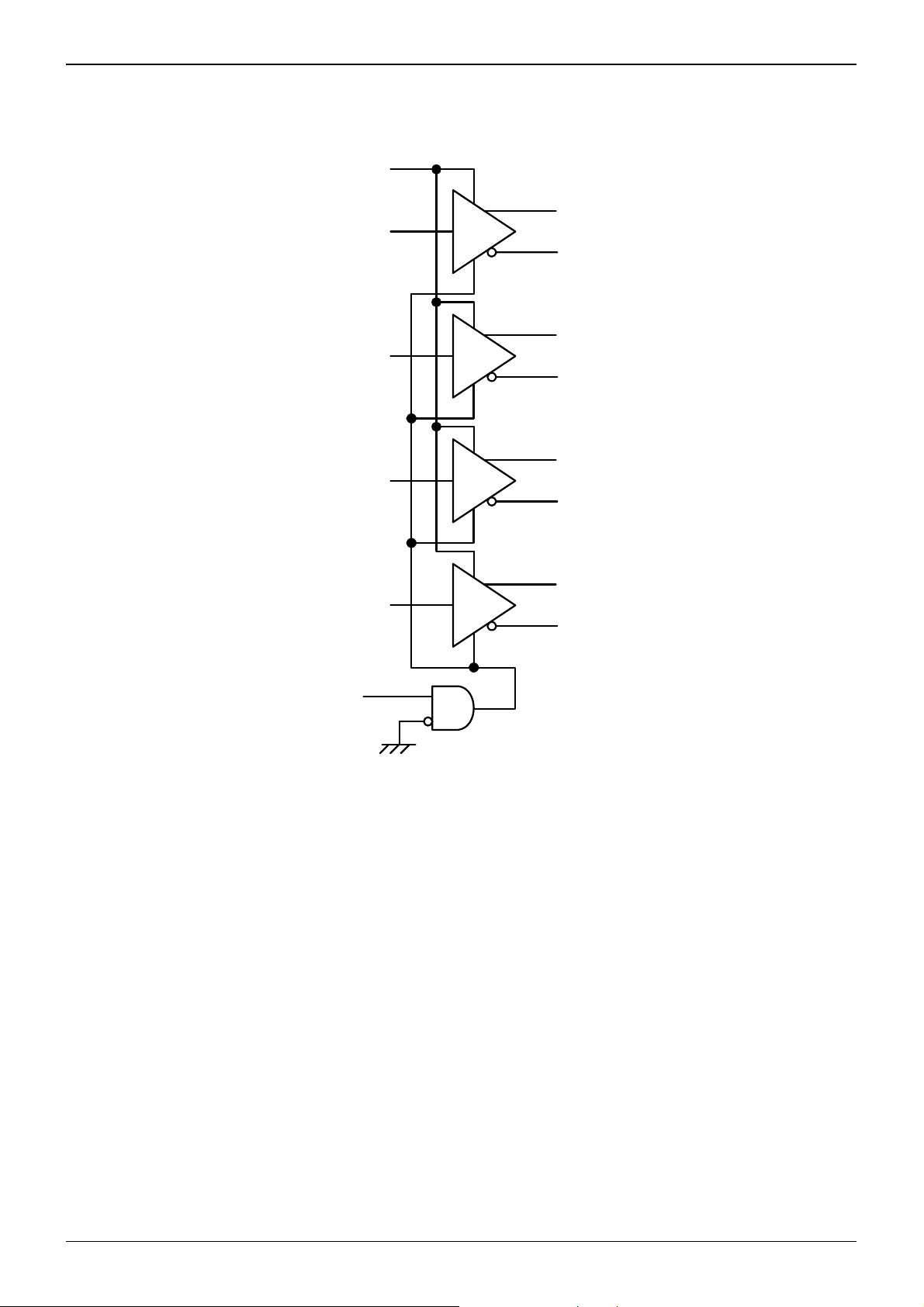
●Block Diagram
Technical Note
EN
SL
IN1
D
IN2
D
IN3
D
IN4
D
Fig.1. Block Diagram
DOUT1+
D1
D2
D3
D4
D
OUT1-
DOUT2+
D
OUT2-
DOUT3+
OUT3-
D
DOUT4+
D
OUT4-
www.rohm.com
© 2011 ROHM Co., Ltd. All rights reserved.
2/11
2011.12 - Rev.
BU90LV047A
A
A
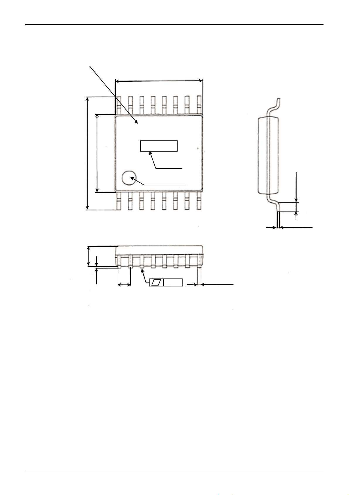
●SSOP-B16 Package Outline and Specification
Product No.
16 9
6.4±0.3
4.4±0.2
1 8
1.15±0.1
0.10
0.65
Fig.2. SSOP-B16 Package Outline and Specification
5.0±0.2
LV47
1PIN MARK
Lot No.
0.10
Technical Note
0.22±0.1
(UNIT:mm)
0.3MIN
0.15±0.1
www.rohm.com
© 2011 ROHM Co., Ltd. All rights reserved.
3/11
2011.12 - Rev.

BU90LV047A
A
●Pin Configuration
EN
D
IN1 2
D
IN2 3
CC 4
V
GND
D
IN3 6
IN4 7
D
SL
1
5
8
Fig.3. Pin Diagram (Top View)
DOUT1-16
D
D
D
D
D
D
D
Technical Note
OUT1+15
OUT2+14
OUT2-13
OUT3-12
OUT3+11
OUT4+10
OUT4-9
www.rohm.com
© 2011 ROHM Co., Ltd. All rights reserved.
4/11
2011.12 - Rev.

BU90LV047A
A
●Pin Description
Table 1 : Pin Description
Pin Name Pin No. Type Descriptions
Technical Note
DIN 2, 3, 6, 7
DOUT+ 10, 11, 14, 15
DOUT- 9, 12, 13, 16
SL 8
EN 1
VCC 4
GND 5
●Function Description
INPUT OUTPUTS
EN SL DIN DOUT+ DOUT-
LVCMOS In
LVDS Out
LVDS Out
LVCMOS In
LVCMOS In
Power
GND
Driver input pin, LVCMOS compatible
Non-inverting driver output pin,
LVDS levels
Inverting driver output pin, LVDS levels
Swing Level select pin : When SL is high, the driver is reduce swing
level (200mV). When SL is low or open, the driver is normal swing
level (350mV).
Driver enable pin: When EN is low or open, the driver is disabled.
When EN is high, the driver is enabled.
Power supply pin, 3.3V±0.3V
Ground pin
Swing Level
H L or Open
H H
All other combinations of
EN, SL inputs
L L H
350mV
H H L
L L H
200mV
H H L
X Z Z
www.rohm.com
© 2011 ROHM Co., Ltd. All rights reserved.
5/11
2011.12 - Rev.

BU90LV047A
A
●Absolute Maximum Ratings
Item Symbol
Value
Min. Max.
Supply voltage VCC -0.3 4.0 V
Input voltage VIN -0.3 VCC+0.3 V
Output voltage VOUT -0.3 VCC+0.3 V
Storage temperature range Tstg -55 125 ℃
●Package Power
Package PD(mW) DERATING(mW/℃)
400 4.0
SSOP-B16
450*2
※1 At temperature Ta > 25℃
※2 Package power when mounting on the PCB board.
The size of PCB board :70×70×1.6(mm
The material of PCB board :The FR4 glass epoxy board.(3% or less copper foil area)
3
)
●Recommended Operating Conditions
Item Symbol
Value
Min. Typ. Max.
Unit
1
※
2
※
4.5
Unit Condition
Technical Note
Supply voltage
Operating temperature range
VCC 3.0 3.3 3.6 V
Topr -40 - 85 ℃
www.rohm.com
© 2011 ROHM Co., Ltd. All rights reserved.
6/11
2011.12 - Rev.

BU90LV047A
A
●DC Characteristics
Parameter Symbol Conditions Pin Min Typ Max Units
Technical Note
Differential Output Voltage V
Output High Voltage V
Output Low Voltage V
Differential Output Voltage V
Output High Voltage V
Output Low Voltage V
Change in Magnitude of VOD for
Complementary Output States
Offset Voltage VOS 1.125 1.25 1.375 V
Change in Magnitude of Vos for
Complementary Output States
Input High Voltage VIH
Input Low Voltage VIL SL GND -
Input Current II
OD1
SL=
SL=
GND, R
V
CC
- 1.42 1.6 V
OH
1
0.90 1.08 - V
OL1
OD2
- 1.35 1.50 V
OH2
1.00 1.15 - V
OL2
= 100Ω (Fig.4)
L
, RL = 100Ω (Fig.4)
D
D
OUT+
△VOD
SL = V
R
L
△V
- 1 25 |mV|
OS
or GND,
CC
= 100Ω (Fig.4)
D
= 0V or VCC,
V
IN
Other Input = V
or GND
CC
EN -10 - +10 μA
250 350 450 mV
120 200 300 mV
OUT-
- 1 35 |mV|
V
CC
IN,
×0.8
- V
×0.2
CC
V
CC
V
V
Input Clamp Voltage VCL ICL = -18mA -1.5 -0.8 - V
ENABLED,
Output Short Circuit Current IOS
Differential Output Short Circuit
Current
Power-off Leakage I
No Load Supply Current Drivers
Enabled
Load Supply Current Drivers
Enabled
No Load Supply Current Drivers
Disabled
I
OSD
I
I
I
OFF
CC
CCL
CCZ
DIN = VCC, D
D
= GND, D
IN
ENABLED, VOD = 0V - -5.4 -9.0 mA
V
= 0V or 3.6V,
OUT
V
=0V or Open
CC
DIN = VCC or GND
R
= 100Ω All Channels,
L
D
= VCC or GND (all outputs)
IN
= VCC or GND,
D
IN
EN = GND, SL = GND
OUT+
OUT-
= 0V or
= 0V
D
D
OUT-
OUT+
V
CC
- -5.4 -9.0 mA
-20 ±1 +20
μA
- 20 - mA
- 20 - mA
- 3 - mA
www.rohm.com
© 2011 ROHM Co., Ltd. All rights reserved.
7/11
2011.12 - Rev.

BU90LV047A
A
●Switching Characteristics
= +3.3V ±0.3V, T
V
CC
Parameter Symbol Conditions Min Typ Max Units
= -40℃ to +85℃
opr
Technical Note
Differential Propagation Delay
High to Low
Differential Propagation Delay
Low to High
Differential Pulse Skew
– t
|t
PHLD
PLHD
|
Channel-to-Channel Skew t
Differential Part to Part Skew t
Differential Part to Part Skew t
Rise Time t
Fall Time t
Disable Time High to Z t
Disable Time Low to Z t
Enable Time Z to High t
Enable Time Z to Low t
Maximum Operating Frequency f
Vcc
GND S1
IN
D
D
Driver ENABLED
Fig.4. Driver VOD and VOS Test Circuit
t
PHLD
t
0.5 1.7 2.8 ns
PLHD
0 0.3 0.4 ns
t
SKD1
0 0.4 0.5 ns
SKD2
SKD3
SKD4
TLH
THL
PHZ
PLZ
PZH
PZL
Max
R
= 100Ω, CL = 15pF
L
(Fig.5 and Fig.6)
0 - 1.0 ns
0 - 1.2 ns
- 0.5 1.5 ns
- 0.5 1.5 ns
- 2 5 ns
R
= 100Ω, CL = 15pF
L
(Fig.7 and Fig.8)
- 3 7 ns
- 3 7 ns
250 - - MHz
D
OUT+
RL/2
RL/2
D
VOS
OUT-
V
OD
0.5 1.7 2.8 ns
- 2 5 ns
www.rohm.com
© 2011 ROHM Co., Ltd. All rights reserved.
8/11
2011.12 - Rev.

BU90LV047A
A
CL
Generator RL
DIN
50Ω
D
Driver ENABLED
CL
Fig.5. Driver Propagation Delay and Transition Time Test Circuit
DIN
1.5V
1.5V
tPHLD
0V
DOUT-
OUT+
D
tPLHD
0V(Differential)
DIFF
V
20%
80%
0V
VDIFF = DOUT+ - DOUT-
80%
0V
20%
tTLH
tTHL
Fig.6. Driver Propagation Delay and Transition T ime W aveforms
CL
VCC
GND
IN
D
D
Generator
50Ω
EN
1/ 4 BU90LV 047A
CL
Fig.7. Driver 3-STATE Delay Test Circuit
DOUT+
D
OUT-
50Ω
50Ω
3V
0V
DOUT+
OUT-
D
V
VOL
+1.2V
Technical Note
OH
www.rohm.com
© 2011 ROHM Co., Ltd. All rights reserved.
9/11
2011.12 - Rev.

BU90LV047A
A
Parameter Measurement Information (Continued)
WHEN SL = L or Open
DOUT+ WHEN DIN = Vcc
D
OUT+ WHEN DIN = GND
D
D
EN
OUT- WHEN DIN = GND
OUT- WHEN DIN = Vcc
Typical Application
ENABLE
DATA
INPUT
1/4 BU90LV047A
Typical Application (Continued)
SINGLE-ENDED
DIFFERENTIAL OUTPUT
DIN
DOUT-
OUT+
D
D
OUT+ - DOUT-
1.5V
50%
tPHZ
tPLZ tPZL
Fig.8. Driver 3-STATE Delay Waveform
RT
100Ω
Fig.9. Point-to-Point Application
|VOD|
0V(DIFF.)
0V
+VOD
-VOD
Fig.10. Driver Output Levels
1.5V
tPZH
50%
50%50%
1/4 BU90LV048
3V
0V
V
OH
VOS (1.25V typical)
VOL
+V
SS
Technical Note
3V
0V
OH
V
1.2V
1.2V
V
OL
DATA
OUTPUT
www.rohm.com
© 2011 ROHM Co., Ltd. All rights reserved.
10/11
2011.12 - Rev.

BU90LV047A
A
●Ordering part number
B U 9 0 L V 0 4 7 A - E 2
Part No. Part No.
SSOP-B16
4.4±0.2
6.4±0.3
1.15±0.1
0.10
90LV047A (Package: SSOP-B16)
5.0±0.2
16
1
0.65
9
0.3Min.
8
0.15±0.1
0.1
0.22±0.1
(Unit : mm)
<Tape and Reel information>
Embossed carrier tapeTape
Quantity
Direction
of feed
2500pcs
E2
The direction is the 1pin of product is at the upper left when you hold
()
reel on the left hand and you pull out the tape on the right hand
Reel
1pin
Order quantity needs to be multiple of the minimum quantity.
∗
Packaging and forming specification
Direction of feed
Technical Note
www.rohm.com
© 2011 ROHM Co., Ltd. All rights reserved.
11/11
2011.12 - Rev.

Notes
No copying or reproduction of this document, in part or in whole, is permitted without the
consent of ROHM Co.,Ltd.
The content specied herein is subject to change for improvement without notice.
The content specied herein is for the purpose of introducing ROHM's products (hereinafter
"Products"). If you wish to use any such Product, please be sure to refer to the specications,
which can be obtained from ROHM upon request.
Examples of application circuits, circuit constants and any other information contained herein
illustrate the standard usage and operations of the Products. The peripheral conditions must
be taken into account when designing circuits for mass production.
Great care was taken in ensuring the accuracy of the information specied in this document.
However, should you incur any damage arising from any inaccuracy or misprint of such
information, ROHM shall bear no responsibility for such damage.
The technical information specied herein is intended only to show the typical functions of and
examples of application circuits for the Products. ROHM does not grant you, explicitly or
implicitly, any license to use or exercise intellectual property or other rights held by ROHM and
other parties. ROHM shall bear no responsibility whatsoever for any dispute arising from the
use of such technical information.
The Products specied in this document are intended to be used with general-use electronic
equipment or devices (such as audio visual equipment, ofce-automation equipment, communication devices, electronic appliances and amusement devices).
The Products specied in this document are not designed to be radiation tolerant.
While ROHM always makes efforts to enhance the quality and reliability of its Products, a
Product may fail or malfunction for a variety of reasons.
Please be sure to implement in your equipment using the Products safety measures to guard
against the possibility of physical injury, re or any other damage caused in the event of the
failure of any Product, such as derating, redundancy, re control and fail-safe designs. ROHM
shall bear no responsibility whatsoever for your use of any Product outside of the prescribed
scope or not in accordance with the instruction manual.
The Products are not designed or manufactured to be used with any equipment, device or
system which requires an extremely high level of reliability the failure or malfunction of which
may result in a direct threat to human life or create a risk of human injury (such as a medical
instrument, transportation equipment, aerospace machinery, nuclear-reactor controller, fuelcontroller or other safety device). ROHM shall bear no responsibility in any way for use of any
of the Products for the above special purposes. If a Product is intended to be used for any
such special purpose, please contact a ROHM sales representative before purchasing.
If you intend to export or ship overseas any Product or technology specied herein that may
be controlled under the Foreign Exchange and the Foreign Trade Law, you will be required to
obtain a license or permit under the Law.
Notice
Thank you for your accessing to ROHM product informations.
More detail product informations and catalogs are available, please contact us.
ROHM Customer Support System
www.rohm.com
© 2012 ROHM Co., Ltd. All rights reserved.
http://www.rohm.com/contact/
R1120
A
 Loading...