

1/4
Structure Silicon Monolithic Integrated Circuit
Function Synchronous Rectifier Step-down DC-DC Converter
Product
Function - Input voltage range 2.5V ~ 4.5V
- Output voltage range 0.95 V ~ 4.5V(REF input voltage range 0.5V~VIN)
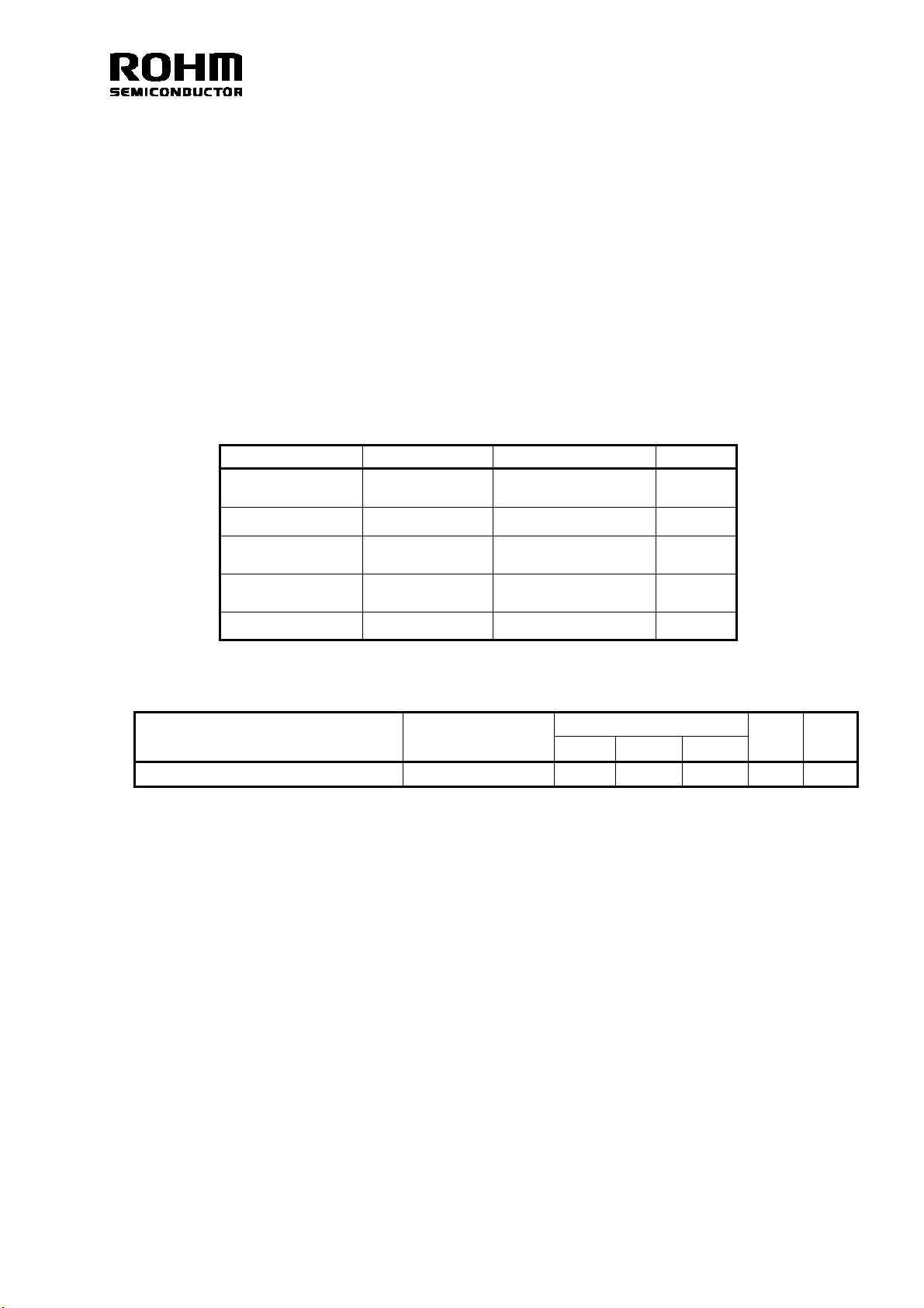
Absolute Maximum rating (Ta=25c)
(*1) When mounted on the specified PCB (50 mm x 58 mm ). Deducted by 4.8m W/c when used over Ta=25c.
BU9006GUZ
- Current mode control
- Integrated output FET synchronous rectifier step-down DC-DC converter
- Switching frequency 2.0MHz typ.
- Maximum output current 750mA (Switching regulator part)
- Maximum output current 1200mA (Bypass switch part)
- PchFET on resistance at bypass mode: (70mohm) typ.
- 1.6mm x 1.6mm, t=0.4mm MAX, WLCSP
Item Symbol Rating Unit
Maximum input
power supply voltage
Power dissipation Pd 0.48(*1) W
Operating temperature
range
Storage temperature
range
Junction temperature Tjmax +125 C
VIN 7 V
Topr -35 ~ +85 C
Tstg -55 ~ +125 C
Operating range (Ta=25c)
Item Symbol
Power supply voltage
VIN
Rating
Min. Typ. Max.
2.5 - 4.5 V
Unit
Condit
ion
REV. A
2/4
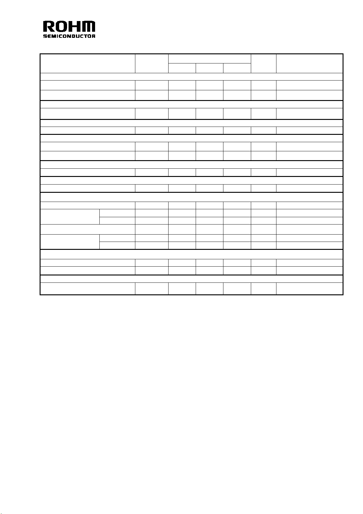
Electrical characteristics
(unless otherwise specified IN=3.6[v], Ta=25[c])
Item Symbol
Min. Typ. Max.
Rating
Unit Condition
[Switching regulator part]
Output voltage 1
Output voltage 2
VOUT1 1.15 1.20 1.25
VOUT2 1.45 1.50 1.55
V REFIN=0.60 V
V REFIN=0.75 V
[Soft start part]
Soft start time Tss -
40 70
usec
[Oscillator circuit]
Switching frequency fosc 1.5 2.0 2.5 MHz
[Driver part]
PchFET on resistance RonP
NchFET on resistance RonN
- 300 500 mΩ
- 250 450 mΩ
[Bypass switch part]
On resistance RBYP - 70 120 mΩ
[Error Amp part]
REF input bias current IAMPIN - 0 500 nA
[Control pin part]
SHDN pin pull down resistor RSHDN 0.5 1 2 MΩ
SHDN pin control
voltage
Operation VSHDNH 1.4 - VIN V
Non operation
VSHDNL 0 - 0.4 V
HP pin pull down resistor RHP 0.5 1 2 MΩ
HP pin control
voltage
Operation VHPH 1.4 - VIN V
Non operation
VHPL 0 - 0.4 V
【UVLO】
Release voltage threshold Uvth 1.95 2.2 2.45 V
Hysteresis Uvhy 70 90 110 mV
[Circuit current]
Circuit current at shutdown IIN - 0 10 uA SHDN=0V
* No design for durability against radiation
REV. A

3/4
Block diagram
REF
HP
SHDN
External dimention/Pin layout
VREF UVLO TSD
SLOPE
CURRENT SENSE
+
CLAMP
IN
+
+
9006
A
LOT No.
B
C
Pin number/name/function
IN
IN
OUT
OUT
+
-
OSC
DRIVER/
CONTROL
LOGIC
LX
GND
123
GND HP REF
LX SHDN IN
IN OUT OUT
Pin layout (TOP VIEW)
Pin nr Name Function
A1 GND GND pin
A2 HP Bypass switch on pin
A3 REF Reference voltage input pin
B1 LX Inductor connection pin
B2 SHDN Shutdown pin
B3 IN
C1 IN
C2 OUT
C3 OUT
Power supply input pin
Output pin
REV. A

4/4
Operation Notes
1) Absolute maximum ratings
An excess in the absolute maximum rating, such as supply voltage, temperature range of operating conditions, etc., can
break down the devices, thus making impossible to identify breaking mode, such as a short circuit or an open circuit.
If any over rated values will expect to exceed the absolute maximum ratings, consider adding circuit protection devices,
such as fuses.
2) GND voltage
The potential of GND pin must be minimum potential in all condition. As an exception, the circuit design allows voltages
up to -0.3 V to be applied to the IC pin.
3) Thermal design
Use a thermal design that allows for a sufficient margin in light of the power dissipation (Pd) in actual operating conditions.
4) Inter-pin shorts and mounting errors
Use caution when positioning the IC for mounting on printed circuit boards. The IC may be damaged if there is any
connection error or if pins are shorted together.
5) Actions in strong electromagnetic field
Use caution when using the IC in the presence of a strong electromagnetic field as doing so may cause the IC to malfunction.
6) Mutual impedance
Power supply and ground wiring should reflect consideration of the need to lower mutual impedance and minimize ripple
as much as possible (by making wiring as short and thick as possible or rejecting ripple by incorporating inductance
and capacitance).
7) Thermal shutdown Circuit (TSD Circuit)
This model IC has a built-in TSD circuit. This circuit is only to cut off the IC from thermal runaway, and has not been
design to protect or guarantee the IC. Therefore, the user should not plan to activate this circuit with continued operation
in mind.
8) Regarding input pin of the IC
This monolithic IC contains P+ isolation and P substrate layers between adjacent elements in order to keep them isolated.
P-N junctions are formed at the intersection of these P layers with the N layers of other elements, creating a parasitic diode
or transistor. For example, as shown in the figures below, the relation between each potential is as follows:
When GND > Pin A and GND > Pin B, the P-N junction operates as a parasitic diode.
When GND > Pin B, the P-N junction operates as a parasitic transistor.
Parasitic diodes can occur inevitable in the structure of the IC. The operation of parasitic diodes can result in
mutual interference among circuits, operational faults, or physical damage. Accordingly, methods by which parasitic
diodes operate, such as applying a voltage that is lower than the GND (P substrate) voltage to an input pin, should not be used.
9) Mounting Condition
As mounting condition to the substrate may cause the affect to the electrical character of IC. The design margin
for the shift value as mount is required, considering the evaluation result for IC to mount the substrate you will use.
10) External Components
The IC evaluation with the external components you will use is required to check the margin within all operating
condition. Because some external inductors and capacitors change its character drastically depending on the DC
current, DC voltage, temperature, and so on.
REV. A

Notes
No copying or reproduction of this document, in part or in whole, is permitted without the
consent of ROHM Co.,Ltd.
The content specied herein is subject to change for improvement without notice.
The content specied herein is for the purpose of introducing ROHM's products (hereinafter
"Products"). If you wish to use any such Product, please be sure to refer to the specications,
which can be obtained from ROHM upon request.
Examples of application circuits, circuit constants and any other information contained herein
illustrate the standard usage and operations of the Products. The peripheral conditions must
be taken into account when designing circuits for mass production.
Great care was taken in ensuring the accuracy of the information specied in this document.
However, should you incur any damage arising from any inaccuracy or misprint of such
information, ROHM shall bear no responsibility for such damage.
The technical information specied herein is intended only to show the typical functions of and
examples of application circuits for the Products. ROHM does not grant you, explicitly or
implicitly, any license to use or exercise intellectual property or other rights held by ROHM and
other parties. ROHM shall bear no responsibility whatsoever for any dispute arising from the
use of such technical information.
Notice
The Products specied in this document are intended to be used with general-use electronic
equipment or devices (such as audio visual equipment, ofce-automation equipment, communication devices, electronic appliances and amusement devices).
The Products specied in this document are not designed to be radiation tolerant.
While ROHM always makes efforts to enhance the quality and reliability of its Products, a
Product may fail or malfunction for a variety of reasons.
Please be sure to implement in your equipment using the Products safety measures to guard
against the possibility of physical injury, re or any other damage caused in the event of the
failure of any Product, such as derating, redundancy, re control and fail-safe designs. ROHM
shall bear no responsibility whatsoever for your use of any Product outside of the prescribed
scope or not in accordance with the instruction manual.
The Products are not designed or manufactured to be used with any equipment, device or
system which requires an extremely high level of reliability the failure or malfunction of which
may result in a direct threat to human life or create a risk of human injury (such as a medical
instrument, transportation equipment, aerospace machinery, nuclear-reactor controller, fuelcontroller or other safety device). ROHM shall bear no responsibility in any way for use of any
of the Products for the above special purposes. If a Product is intended to be used for any
such special purpose, please contact a ROHM sales representative before purchasing.
If you intend to export or ship overseas any Product or technology specied herein that may
be controlled under the Foreign Exchange and the Foreign Trade Law, you will be required to
obtain a license or permit under the Law.
Thank you for your accessing to ROHM product informations.
More detail product informations and catalogs are available, please contact us.
ROHM Customer Support System
www.rohm.com
© 2010 ROHM Co., Ltd. All rights reserved.
http://www.rohm.com/contact/
R1010
A
 Loading...