

192
Communication ICs
DTMF receiver for telephones
BU8872 / BU8872FS
The BU8872 and BU8872FS are DTMF receiver ICs developed for use in telephone answering machines, and convert
16 different types of DTMF signals into 4-bit binary serial data. In addition to a compact 8-pin DIP (BU8872) or 16-pin
SSOP (BU8872FS) package, these receivers feature a wide dynamic range, eliminating the need for an external input
amplifier. Expertise from a number of companies has been incorporated into these products to enable guard time control
through a host microcomputer.
Applications
Telephone answering machines
Features
1) Dynamic range of 45dB. (internal AGC)
2) 4-bit binary serial data output.
3) Guard time can be controlled through host microcomputer.
4) Input pins equipped with hysteresis. (ACK pin)
5) 4.19MHz ceramic resonator or crystal resonator can
be used.
6) 8-pin DIP package. (BU8872)
16-pin SSOP package. (BU8872FS)
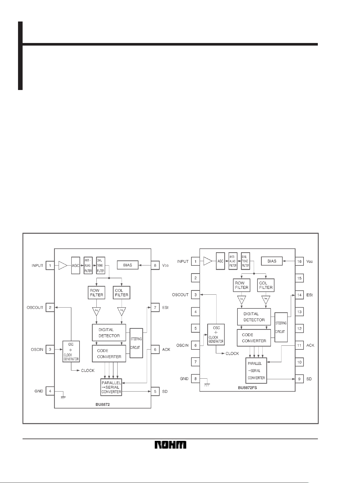
Block diagram
193
Communication ICs BU8872 / BU8872FS
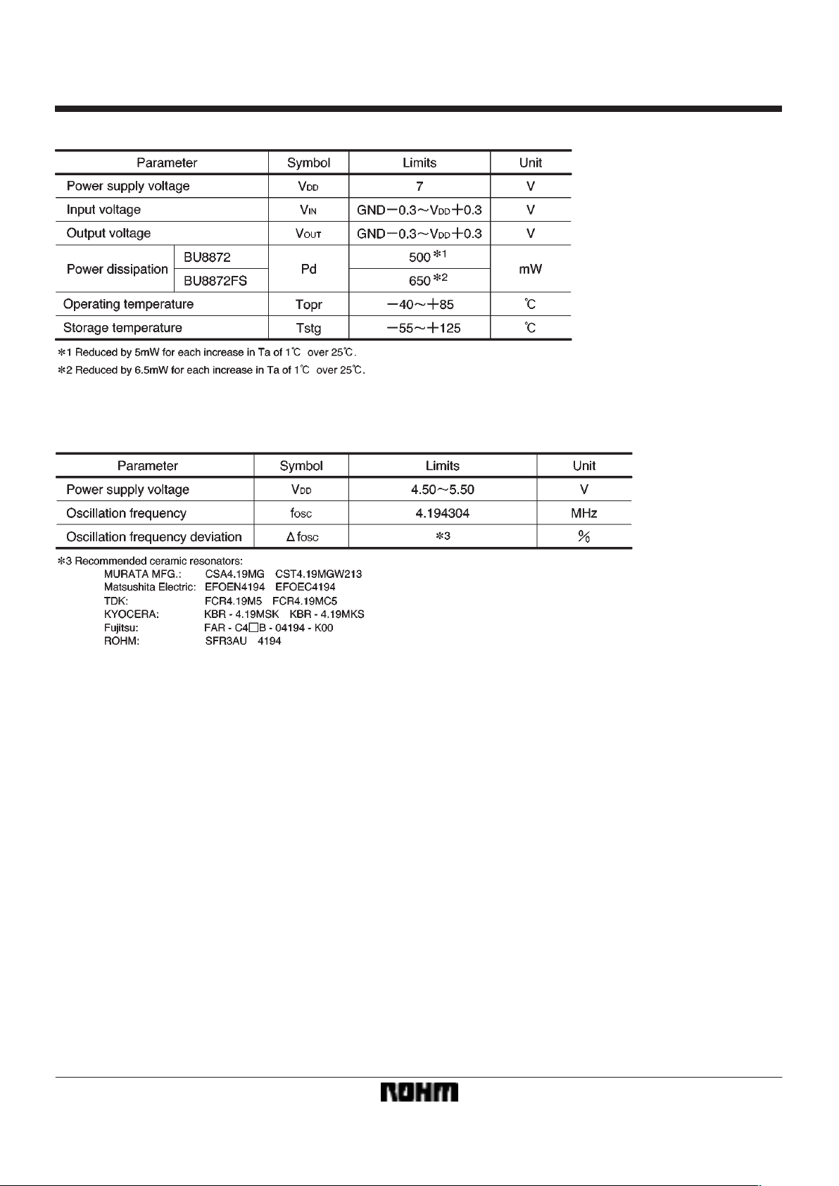
FAbsolute maximum ratings (Ta=25_C)
FRecommended operating conditions (Ta=25_C)
194
Communication ICs BU8872 / BU8872FS
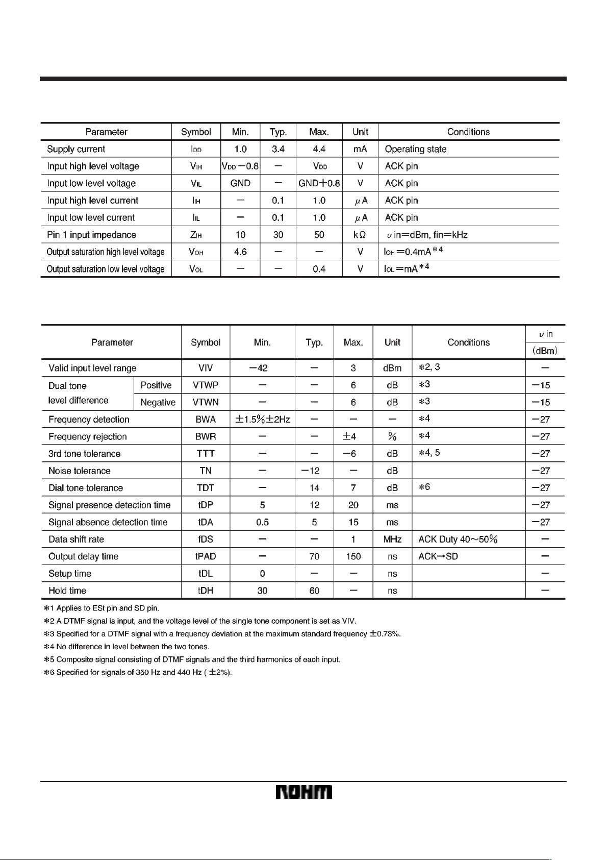
FElectrical characteristics
DC characteristics (unless otherwise noted, Ta=25_C, V
DD=5.0V)
AC characteristics (unless otherwise noted, Ta=25_C, V
DD=5.0V)

195
Communication ICs BU8872 / BU8872FS
Pin descriptions
Input / output circuits

196
Communication ICs BU8872 / BU8872FS
Circuit operation
A DTMF signal is supplied to the INPUT pin and applied
to a pair of 6th-order bandpass filters, which separate the
DTMF signal into its high (COL) and low (ROW) frequencies. The separated tones are converted into square
waves and fed to a digital detector. (See the block diagram.)
The digital detector checks the two tones to see if they
are within the valid DTMF frequency bands. If they are,
it sends a DETECT signal to the steering circuit, and
sends the appropriate column and row address signals
to a code converter.
The code converter encodes the received and detected
DTMF signal, and outputs an ENABLE signal to the
steering circuit.
Based on the DETECT and ENABLE signals, the steering circuit outputs an Early Steering (ESt) signal, which
sets the ESt pin to HIGH, indicating that a valid DTMF
signal has been detected.
If a series of pulses is input at the ACK pin while ESt is
HIGH, a decoded DTMF signal is output to the SD pin as
a binary code. (See Figure 2 for the overall timing.)
If a pulse sequence is input at the ACK pin, the data is
latched at the rising edge of the first pulse by a parallelserial converter, and at the same time, the LSB is output
from the SD pin. Following this, three bits of data are output from the SD pin for each bit of each pulse in the pulse
sequence input from the ACK pin. As a result, a total of
four bits of data are output for the four pulses. (See Figure 3 for the ACK and SD timing.)
If the pulse sequence input to the ACK pin consists of
three or fewer pulses, the next DTMF input cannot be decoded properly . Any ACK pulses in excess of four are ignored until ESt goes HIGH again.
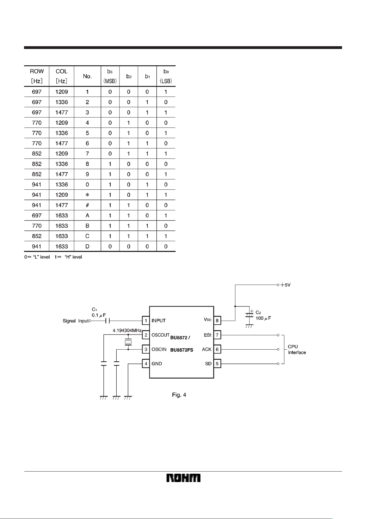
Table 1 shows the format of serial data output from the
SD pin.
197
Communication ICs BU8872 / BU8872FS
Table 1. Serial data correspondence table
Application example

198
Communication ICs BU8872 / BU8872FS
FOperation notes
(1) To prevent latch-ups, we recommend inserting a bypass capacitor (a capacitor between V
DD and GND) close to
the V
DD pin of the device.
(2) If using a pin-type ceramic resonator, connect a CH class capacitor between the OSCIN and OSCOUT pins and
the GND.
(3) This LSI is not equipped with the power-on reset function. Also, since the internal circuit (flip-flop circuit) becomes
unstable at the rising edge of the power supply, the internal circuit is initialized as shown below by the first DTMF sequence received after the rising edge of the power supply . Therefore, input four dummy ACK pulses before the DTMF
reception.
FSelecting attached components
(1) Power supply components
C502 : This is the V
DD bypass capacitor, and is normally
100µF.
JP501 : This is normally shorted. To test the current con-
sumption of the IC, insert a DC ammeter in place
of JP501.
(2) Oscillation components
X501, C551, and C552 : Use a crystal or ceramic resona-
tor with an oscillation frequency of
4.194304MHz. If using a ceramic resonator,
there may be problems with the precision of the
oscillation frequency, so we recommend using
one of the ceramic resonators listed below.
X501 C551 C552
Murata CSA4.19MG 30pF 30pF
CST4.19MGW213 (internal capacitors)
Matsushita EFOEN4194 33pF 33pF
EFOEC4194 (internal capacitors)
TDK FCR4.19M5 33pF 33pF
FCR4.19MC5 (internal capacitors)
Kyocera KBR-4.19MSK 33pF 33pF
KBR-4.19MKS (internal capacitors)
Fujitsu FAR-C4j (internal capacitors)
B-04194-K00
ROHM SFR3AU 4194 (internal capacitors)
C591 : If you are using a dedicated resonator designed
for DTMF receivers, such as the X501, C551, or
C552, capacitor C591 should be left open. If you
are injecting an external clock, X501 should be
omitted and capacitor C591 used in its place.
Typically, this capacitor should be 47nF .

Use these to increase the sensitivity of
the DTMF receiver.
199
Communication ICs BU8872 / BU8872FS
(3) DTMF input
C501 : This is the DC blocking capacitor. Select a ca-
pacitor that will pass DTMF signals (greater
than 697Hz) without significantly attenuating
the signals.
JP592 : If DTMF signals are being input directly, both
ends should be shorted.
C591
R591 R595
C592, C593
(4) ESt output
The ESt guard time is determined by the CPU of the host
computer, but to reduce the load on the host computer,
the guard time can be set using an external circuit, as
shown below.
The relation between a momentary falter in the ESt guard
time (t
GL), a momentary HIGH level in the ESt guard time
(t
GH), and the time constant is shown below. Figure 10
shows a timing diagram for guard times.

200
Communication ICs BU8872 / BU8872FS
Electrical characteristic curves
201
Communication ICs BU8872 / BU8872FS
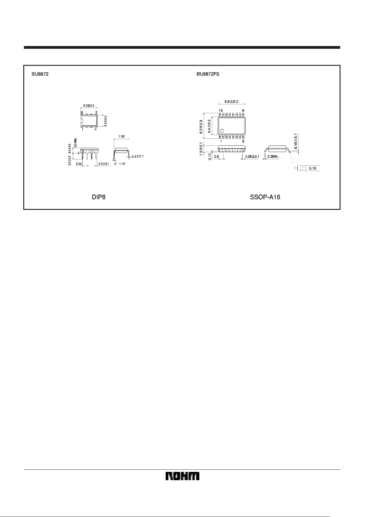
External dimensions (Units: mm)
 Loading...