


MSDL (Mobile Shrink Data Link) Transceivers for Mobile Phones
Data rate 1350Mbps
RGB Interface
BU7964GUW
●Description
BU7964GUW is a differential serial interface connecting mobile phone LCD modules to the host CPU. Unique technology is
utilized for lower power consumption and EMI. MSDL minimizes the number of wires required - an important consideration
in hinge phones - resulting in greater reliability and design flexibility.
●Features
1) MSDL3 high-speed differential interface with a maximum transfer rate of 1350 Mbps.
2) Compatible with24-bit RGB video mode for LCD controller-to-LCD interface.
3) Pixel clock frequency range from 4 to 45MHz.
4) Depending on the data transfer rate, either, two or three differential data channels can be selected.
●Applications
Serial Interface for LCD Display Interface of Mobile Devices Application.
●Absolute Maximum Ratings
Parameter Symbol Ratings Unit Remarks
Power Supply Voltage
Input Voltage VIN
Output Voltage VOUT
Input Current IIN -10 ~ +10 mA -
Output Current IOUT -70 ~ +70 mA -
Preservation Temperature Tstg -55 ~ +125 ℃ -
●Operating Conditions
Parameter Symbol
Supply Voltage for DVDD V
Supply Voltage for MSVDD V
Data Transmission Rate DR 120 - 450 Mbps/ch -
Operating Temperature Range T
DVDD -0.3 ~ +2.5 V -
MSVDD -0.3 ~ +2.5 V -
-0.3 ~ MSVDD+0.3 V I/O terminals of MSVDD line
-0.3 ~ DVDD+0.3 V I/O terminals of DVDD line
-0.3 ~ MSVDD+0.3 V I/O terminals of MSVDD line
-0.3 ~ DVDD+0.3 V I/O terminals of DVDD line
Ratings
Min Typ Max
1.65 1.80 1.95 V
DVDD
1.65 1.80 1.95 V
MSVDD
-30 25 85 ℃ -
opr
Unit Conditions
= V
V
DVDD
No.10058EAT04
MSVDD
www.rohm.com
© 2010 ROHM Co., Ltd. All rights reserved.
1/18
2010.04 - Rev.A

BU7964GUW
●Package View
MARK
0.75±0.1
63-φ0.295±0.05
M
0.05
1PIN
0.08 S
S
AB
BU7964
LOT NO.
5.0±0.1
A
P = 0.5×7
0.5
H
G
F
E
D
C
B
A
23456
1
Fig.1. Package View (VBGA063W50)
78
Technical Note
5.0±0.1
0.9 MAX
S
0.10
0.75±0.1
B
P = 0.5×7
(UNIT:mm)
www.rohm.com
© 2010 ROHM Co., Ltd. All rights reserved.
2/18
2010.04 - Rev.A

BU7964GUW
●Block Diagram
D 0
-
D 0
+
MSVDD
High Speed I/F
Technical Note
DVDD
D 1
D 1
D 2
D 2
CLK
CLK
DRVR
-
+
-
+
-
+
Link
Monitor
Reference
Serial
to
Parallel
PLL
Reset
Generator
Error
Detection
Timing
Generator
Control
Logic
I / F
Logic
PCLK
Control
PD
CPO
PCLK
XSD
LS
F_XS
PLLBW
TEST
DGNDMSGND
Fig.2. Block Diagram
www.rohm.com
© 2010 ROHM Co., Ltd. All rights reserved.
3/18
2010.04 - Rev.A

BU7964GUW
●Pin Layout
1 2 3 4 5 6 7 8
A TEST0 PD19 PD17 PD16 PD14 PD13 PD10 CPO
B PCLK PD18 PD15 PD12 PD11 PD9 PD8
C PD22 PD20 PLL_BW0 DVDD N.C. F_XS PD7 PD6
D PD23 PD21 N.C. DGND DGND DVDD PD4 PD5
E PD25 PD24 DVDD DGND MSGND N.C. PD1 PD3
Technical Note
F PD26 LS0 MSVDD MSGND MSVDD N.C. XSD PD2
G LS1 PLL_BW1 D2- D1- CLK- D0- N.C. PD0
H N.C. N.C. D2+ D1+ CLK+ D0+ DRVR TEST1
Fig.3. Pin Layout (Top View)
www.rohm.com
© 2010 ROHM Co., Ltd. All rights reserved.
4/18
2010.04 - Rev.A

BU7964GUW
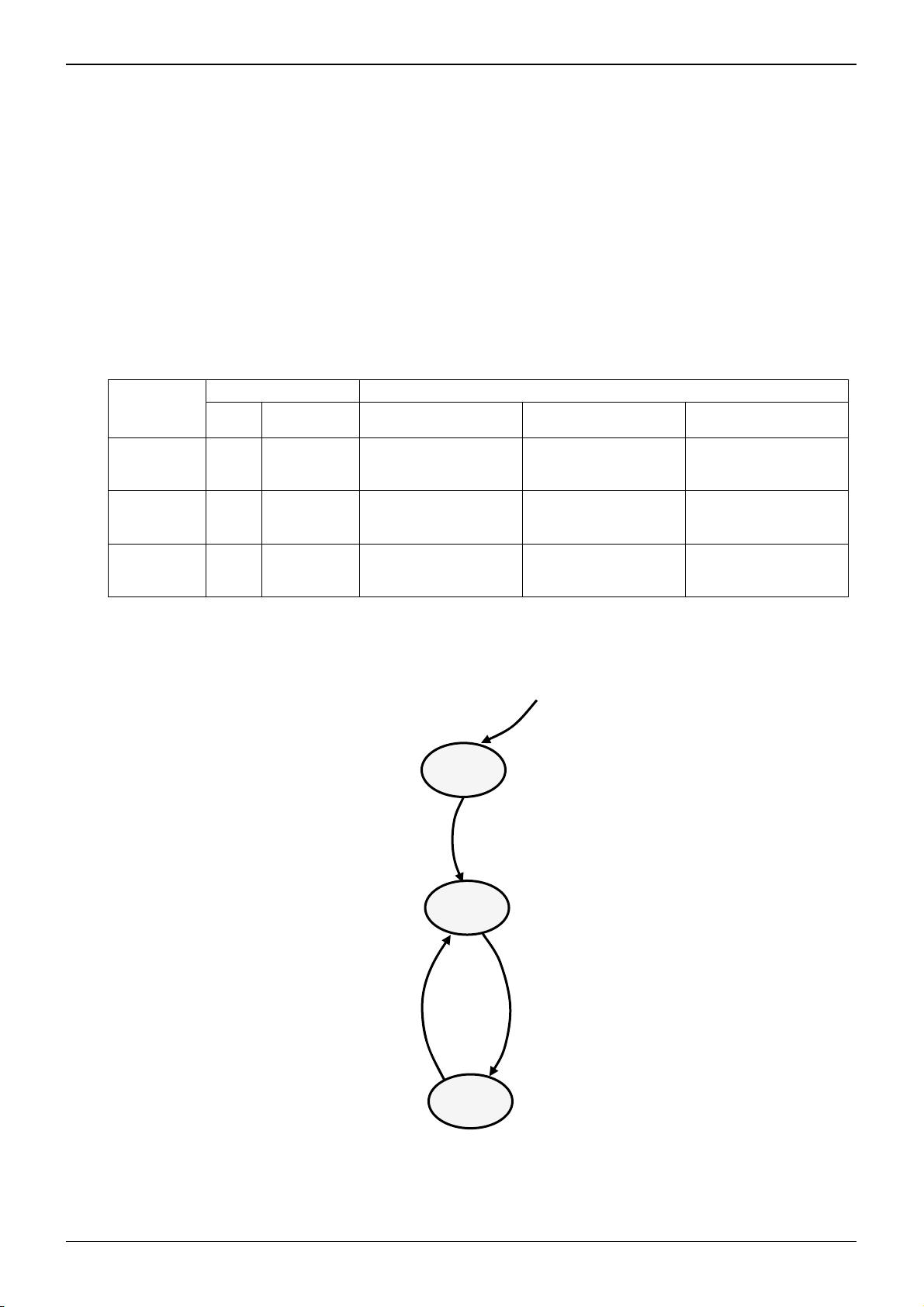
●Pin Functions
Power Supply / Ground: 10-pin
Name Width Functions
DVDD 3 Logic core, CMOS I/O power supply.
MSVDD 2 Analog core power supply.
DGND 3 CMOS I/O and logic core ground.
MSGND 2 Analog core ground.
High-Speed Serial Interface: 8-pin
Name Width Level I/O Functions Shutdown
CLK+ 1 Analog I CLK+pin. Pull Down D
CLK- 1 Analog I CLK-pin. Pull Down D
D0+ 1 Analog I D0+pin. Pull Down D
Technical Note
Table 1. Power Supply and Ground
Table 2. MSDL3
Equivalent
Schematic
D0- 1 Analog I D0-pin. Pull Down D
D1+ 1 Analog I D1+pin. Pull Down D
D1- 1 Analog I D1-pin. Pull Down D
D2+ 1 Analog I D2+pin. Pull Down D
D2- 1 Analog I D2-pin. Pull Down D
Table 3. Analog
Analog: 1-pin
Name Width Level I/O Functions Shutdown
DRVR 1 Analog -
Parallel Data Interface: 29-pin
Name Width Level I/O Functions Shutdown
PCLK 1 CMOS O PCLK interface. ‘L’ C
PD[26:0] 27 CMOS O Parallel data interface. ‘L’ C
CPO 1 CMOS O
10kΩ ± 5% register should be connected between
DRVR and MSGND.
Table 4. Parallel Data Interface
Parity error toggled output, normally ‘L,’ output is
toggled during one PCLK period when a parity error
is detected
- D
‘L’ C
Equivalent
Schematic
Equivalent
Schematic
www.rohm.com
© 2010 ROHM Co., Ltd. All rights reserved.
5/18
2010.04 - Rev.A

BU7964GUW
A
Name Width Level I/O Functions Shutdown
XSD 1 CMOS I
Table 5. Control
Control: 8-pin
Shutdown pin.
‘L’: shutdown.
‘H’: normal operation.
Technical Note
Equivalent
Schematic
Input A
LS0 1
CMOS I
LS1 1
F_XS 1 CMOS I
PLL_BW0 1
CMOS I Selection of PLL bandwidth. Input A
PLL_BW1 1
TEST0 1
Pull
down
TEST1 1 B
B C
DVDD
Selection of the number of data channel and the
data format. Refer to section 0.
* Set the same number of data channel bet
wean the TX device and the RX device.
Selection of CMOS output rising and falling slope
‘L’: slow
‘H’: fast
Test mode pins.
‘L’: normal mode.
I
‘H’: test mode.
Must be open or ‘L.’
DVDD
Fig.4. Equivalent Schematics
DVDD
Input A
Input A
B
Input
MSVDD
D
www.rohm.com
© 2010 ROHM Co., Ltd. All rights reserved.
6/18
2010.04 - Rev.A
BU7964GUW
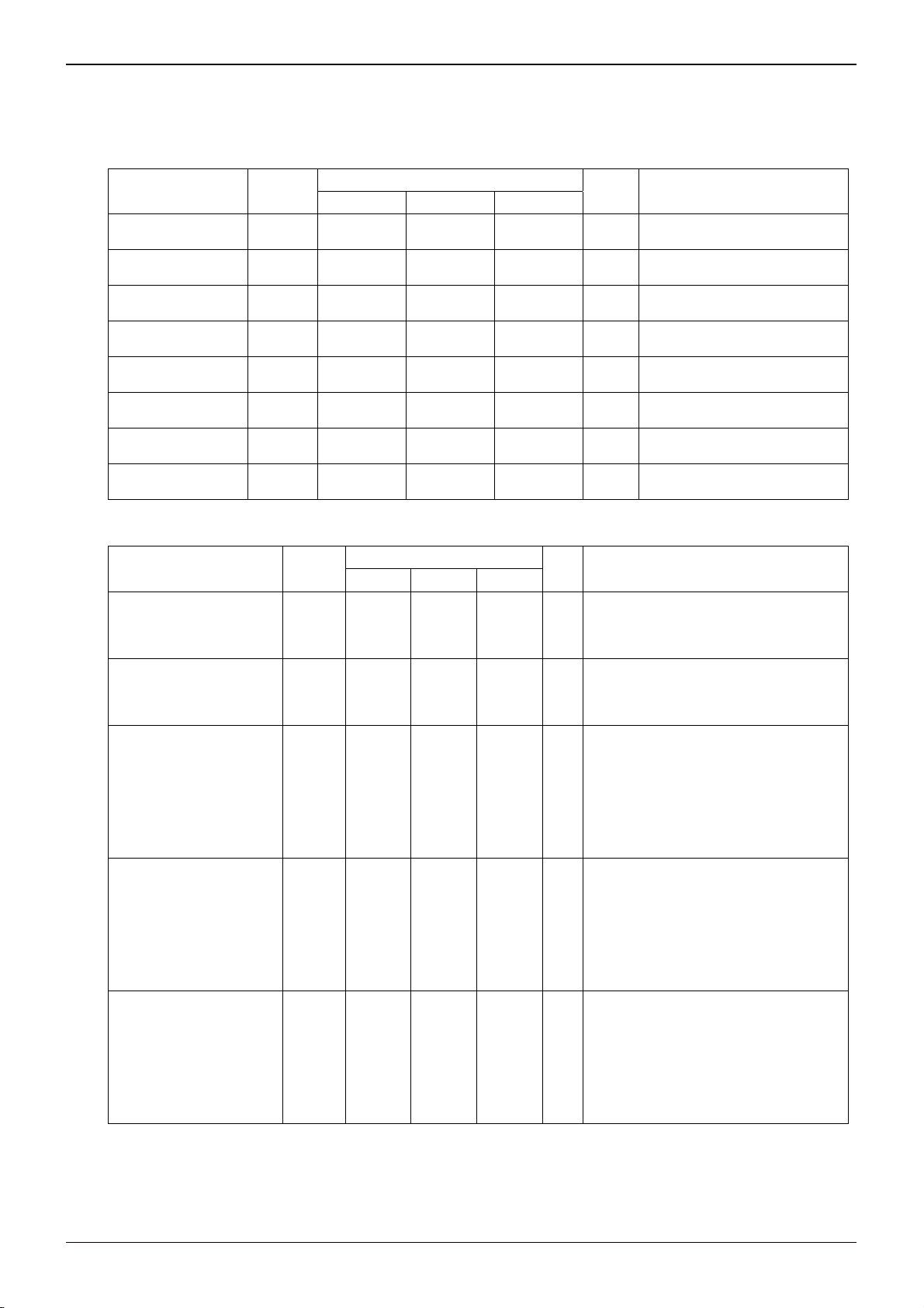
●Operation Control
MSDL3 Channel Count Selection
Pins LS0 and LS1 are used to control the high-speed data channel count and data format. High-speed data channel count,
data format should be the same between the transmitting and receiving devices (the BU7963GUW and BU7964GUW,
respectively). Table 6 shows and Receipt Data rate ranges for the LS pin settings.
Table 6. The Range of The Receipt Data rate
LS1 LS0
‘L’ ‘L’ 1-channel (27-bit format). 4.0-15.0 120-450
‘L’ ‘H’ 2-channel (27-bit format). 8.0-30.0 240-900
‘H’ ‘L’ 3-channel (27-bit format). 12.0-45.0 360-1350
CMOS Output Drivability Selection
F_XS determines output drivability of the parallel data interface. Table 7 shows output drivability.
The Number of Data Channel
Table 7. Output Drivability
The Range of PCLK Input
Frequency [MHz]
The Data Receipt Rate
Technical Note
The Range of
[Mbits/sec]
F_XS
‘L’ 1mA Type
‘H’ 3mA Type
PLL Bandwidth Selection
BU7964GUW controls the range of the CLK+ / CLK− input frequency (= PCLK output frequency) by the setting of the
data format (LS1, and LS0) of the high-speed data channel and the bandwidth setting of PLL_BW0 and PLL_BW1.
Table 8. PLL Bandwidth Selection
LS1 LS0 PLL_BW1 PLL_BW0
‘L’ ‘L’ ‘L’ ‘L’ 4 7
‘L’ ‘L’ ‘L’ ‘H’ 6 11
‘L’ ‘L’ ‘H’ ‘L’ 10 15
‘L’ ‘H’ ‘L’ ‘L’ 8 14
‘L’ ‘H’ ‘L’ ‘H’ 12 22
‘L’ ‘H’ ‘H’ ‘L’ 20 30
‘H’ ‘L’ ‘L’ ‘L’ 12 21
Output Drivability
CLK+/CLK- Frequency Range [MHz]
(PCLK Input Frequency)
Min Max
‘H’ ‘L’ ‘L’ ‘H’ 18 33
‘H’ ‘L’ ‘H’ ‘L’ 30 45
www.rohm.com
© 2010 ROHM Co., Ltd. All rights reserved.
7/18
2010.04 - Rev.A
BU7964GUW
Technical Note
●Power Modes
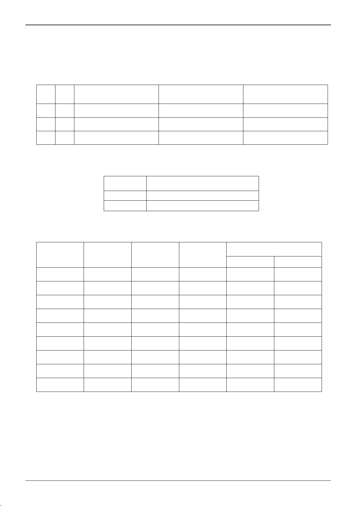
BU7964UW has three power modes.
1) Shutdown Mode
BU7964GUW goes to Shutdown Mode when XSD = ‘L.’ AII logic circuits are
initialized in the Shutdown Mode. All high-speed signaling are pulled down to
MSGND. All parallel data interface output ‘L’.
2) Standby Mode
BU7964GUW goes to a Standby Mode when XSD = ‘H’ and CLK+ / CLK− is Hi-Z. All high-speed signaling inputs sink
DC current in order to pull the pins down to MSGND. BU7964GUW is monitoring V
starts driving high-speed signaling outputs, BU7964GUW detects its V
and switches to Active Mode. In Standby Mode,
CM
of CLK+ / CLK−. When TX device
CM
All parallel data interface output ‘L’.
3) Active Mode
BU7964UW goes to Active Mode when XSD = ‘H’ and VCM is running.
Table 9. Power Modes
Input Operation
Power Mode
XSD
Vcm of
CLK+/CLK-
Functions MSDL3 Terminals Parallel output
Shutdown ‘L’ MSGND Initialized Disabled(Pull-down) Initial value
Standby ‘H’ MSGND MSDL3 Vcm detection
Active ‘H’
Clock input is
4) Power Modes Transition
Fig.5.shows the Transition of power modes.
active
MSDL3 V
monitor.
CM
Normal operation.
(S2P conv)
Shutdown
XSD = ”H”
Standby
XSD = ”L”
MSDL3 Vcm
detection
(Pull-down)
MSDL3 V
Enabled.
monitor.
CM
Initial value
Normal operation
www.rohm.com
© 2010 ROHM Co., Ltd. All rights reserved.
PCLK input
disabled (Hi-z)
Active
Fig.5. Power Modes Transition
8/18
PCLK input
detected
2010.04 - Rev.A

BU7964GUW
/
Technical Note
●Link Error Detection
Detection of Parity Error
BU7964GUW counts the number of ‘H’ bits in PD[26:0] and CP in every pixel information received and detects parity error
as follows:
・There is no parity error occurred if the number of ‘H’ bits in PD[26:0] and CP is odd.
・There is parity error occurred if the number of ‘H’ bits in PD[26:0] and CP is even.
If parity error is detected, BU7964GUW outputs the previous error-free pixel information and discards the invalid pixel
information. At the same time, BU7964GUW toggles CPO during one PCLK period. BU7964GUW outputs initial value, if
the parity error is detected when there is no previous pixel information. Otherwise, BU7964GUW outputs the received
pixel information from the high-speed data channel(s) and CPO keeps ‘L.’
Error correction is not supported in BU7964GUW.
●High-Speed Data Channel Protocols
Fig.6 Fig.7 and Fig.8 show high-speed data channel protocols.
D
0channel
CLK channel
D 0channel
D 1channel
CLK channel
CP
PD26 PD
PD26 PD
D 0channel
D 1channel
D 2channel
25 PD24 PD18PD19PD20PD21PD22PD 23 PD 13PD 14PD15PD16PD17 PD12
Frame start
end
7PD8PD 9PD 10 CPres resPD0PD1
PD2PD3PD4PD5PD6PD
PD 26 PD25PD 11
Fig.6. MSDL3 Protocol for 1-channel Data (27-bit)
PD
25 PD24 PD19PD20PD21PD22PD 23 PD18 PD15PD16PD17
PD13PD14 PD12 PD11 PD3PD4PD5PD6PD7PD8PD9PD10 PD
Frame start/end
res CP CP
2PD26
resres
0PD 1
PD14
Fig.7. MSDL3 Protocol for 2-channel Data (27-bit)
CP PD26 PD25 PD 24 PD19PD20PD21PD22PD23 PD2 CP
res PD18 PD17 PD 16 PD11PD12PD13PD14PD15 PD1 res
res PD10 PD 9PD 8PD3PD4PD5PD6PD7PD0res
PD 26
PD
18
PD 10
CLK channel
Frame start / end
Fig.8. MSDL3 Protocol for 3-channel Data (27-bit)
“res” is reserved bit for the future use, the default state of those is ‘0.’
CP is the parity bit of data payload.
BU7964GUW adds an odd parity on CP of the high-speed channel data.
・When the number of ‘H’ bits in parallel data is even, CP bit is ‘H.’
・When the number of ‘H’ bits in parallel data is odd, CP bit is ‘L.’
www.rohm.com
© 2010 ROHM Co., Ltd. All rights reserved.
9/18
2010.04 - Rev.A
BU7964GUW
●Electrical Characteristics
1) DC Characteristics
Table 10. Digital Input / Output DC Characteristics
Ta=25°C, DVDD=MSVDD=1.80V and DGND=MSGND=0.00V, unless otherwise noted.
Parameter Symbol
Min Typ Max
Limits
‘L’ Input Voltage 1 VIL1 DGND - 0.3 x DVDD V
‘H’ Input Voltage 1 VIH1 0.7 x DVDD - DVDD V
Output ‘L’ Voltage1 VOL1 DGND - 0.3 x DVDD V
Output ‘H’ Voltage1 VOH1 0.7 x DVDD - DVDD V
Output ‘L’ Voltage2 VOL2 DGND - 0.3 x DVDD V
Output ‘H’ Voltage2 VOH2 0.7 x DVDD - DVDD V
Output ‘L’ Voltage3 VOL3 DGND - 0.15 x DVDD V
Output ‘H’ Voltage3 VOH3 0.85 x DVDD - DVDD V
Table 11. Current Consumption
Ta=25°C, DVDD=MSVDD=1.80V and DGND=MSGND=0.00V, unless otherwise noted.
Parameter Symbol
Min Typ Max
Limits
Technical Note
Unit Conditions
XSD, F_XS
PLL_BW[1:0], LS[1:0]Pin
XSD, F_XS
PLL_BW[1:0], LS[1:0]Pin
F_XS=‘L’, IO = 1mA,
PCLK, CPO, PD[26:0]Pin
F_XS=‘L’, IO = -1mA,
PCLK, CPO, PD[26:0]Pin
F_XS=‘H’, IO = 3mA,
PCLK, CPO, PD[26:0]Pin
F_XS=‘H’, IO = -3mA,
PCLK, CPO, PD[26:0]Pin
IO = 100µA,
PCLK, CPO, PD[26:0]Pin
IO = -100µA,
PCLK, CPO, PD[26:0]Pin
Unit Conditions
Shutdown Current I
Standby Current I
Active Current
1-channel / 27-bit Format
Active Current
2-channel / 27-bit Format
Active Current
3-channel / 27- bit Format
op_sht_rx
op_stb_rx
I
op_act_rx1
I
op_act_rx2
I
op_act_rx3
- 0.2 10 µA
- 41.8 90 µA
- 17.6 24.0 mA
- 28.0 36.8 mA
- 36.0 48.6 mA
XSD = ‘L’,
IDVDD + IMSVDD
XSD = ‘H’,
IDVDD + IMSVDD
LS[1:0] = “LL”,
PLL_BW[1:0] = “HL”,
DVDD = MSVDD,
PCLK = 15MHz, XSD = ‘H’,
CL = 10pF,
Total operating current (IDVDD +
IMSVDD) with PD[26:0] outputs toggling
0x2AAAAAA and 0x5555555
LS[1:0] = “LH”,
PLL_BW[1:0] = “HL” ,
DVDD = MSVDD,
PCLK = 30MHz, XSD = ‘H’,
CL = 10pF,
Total operating current (IDVDD +
IMSVDD) with PD[26:0] outputs toggling
0x2AAAAAA and 0x5555555
LS[1:0] = “HL”,
PLL_BW[1:0] = “HL” ,
DVDD = MSVDD,
PCLK = 45MHz, XSD = ‘H’,
CL = 10pF,
Total operating current (IDVDD +
IMSVDD) with PD[26:0] outputs toggling
0x2AAAAAA and 0x5555555
www.rohm.com
© 2010 ROHM Co., Ltd. All rights reserved.
10/18
2010.04 - Rev.A
BU7964GUW
_
R
_
_
K
2) AC Characteristics
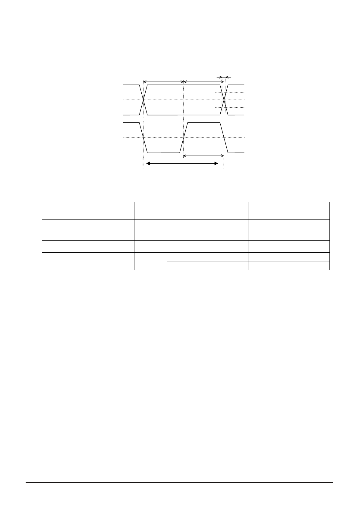
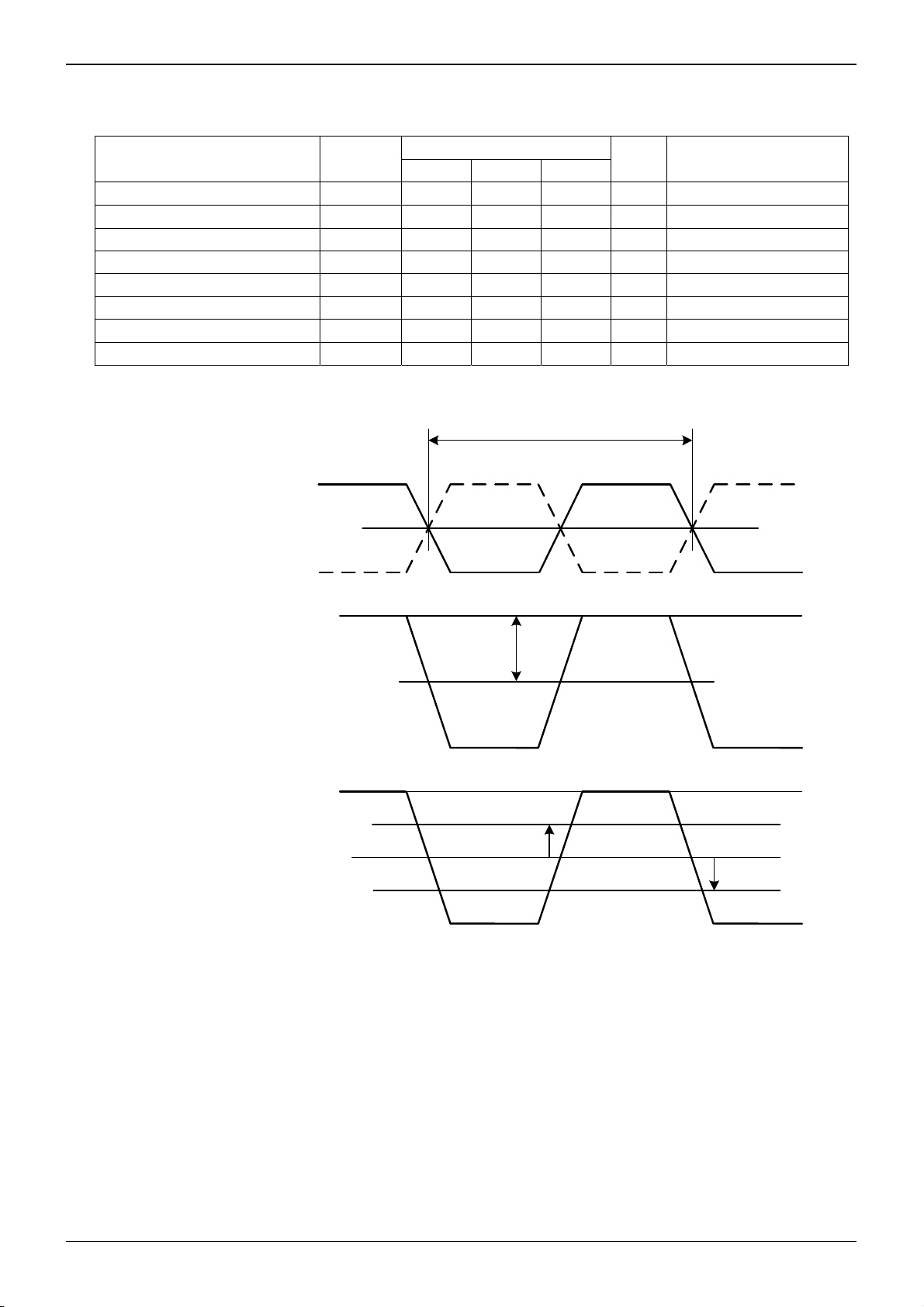
Parallel Data Output Timing
t
R_D
P [2 : 0]
PCL
Fig.9. Parallel Data Output Timing
Table 12. Parallel Data Output AC Timing
Ta=25°C, DVDD=MSVDD=1.80V and DGND=MSGND=0.00V, unless otherwise noted.
Parameter Symbol
PCLK Output Duty Cycle t
Output Data Setup Time t
Output Data Hold Time t
Output Data Rise Time/Fall time
45 50 55 % CL=10pF
RX_DUTY
RX_DS
RX_DH
t
RX_R
t
RX_F
Technical Note
t
R
,
t
R
t
R_D
t
R_DUTY
t
R
PCL
Limits
Min Typ Max
0.41X
t
Rx_PCLK
0.41X
t
Rx_PCLK
- - ns CL=10pF
- - ns CL=10pF
- 9 - ns F_XS=0, CL=10pF
- 3 - ns F_XS=1, CL=10pF
F
0.7×DVDD
0.5×DVDD
0.3×DVDD
0.5×DVDD
Unit Conditions
www.rohm.com
© 2010 ROHM Co., Ltd. All rights reserved.
11/18
2010.04 - Rev.A

BU7964GUW
_
VDD_
X
_
V
_
V
_
VDD_
X
_
V
_
V
y
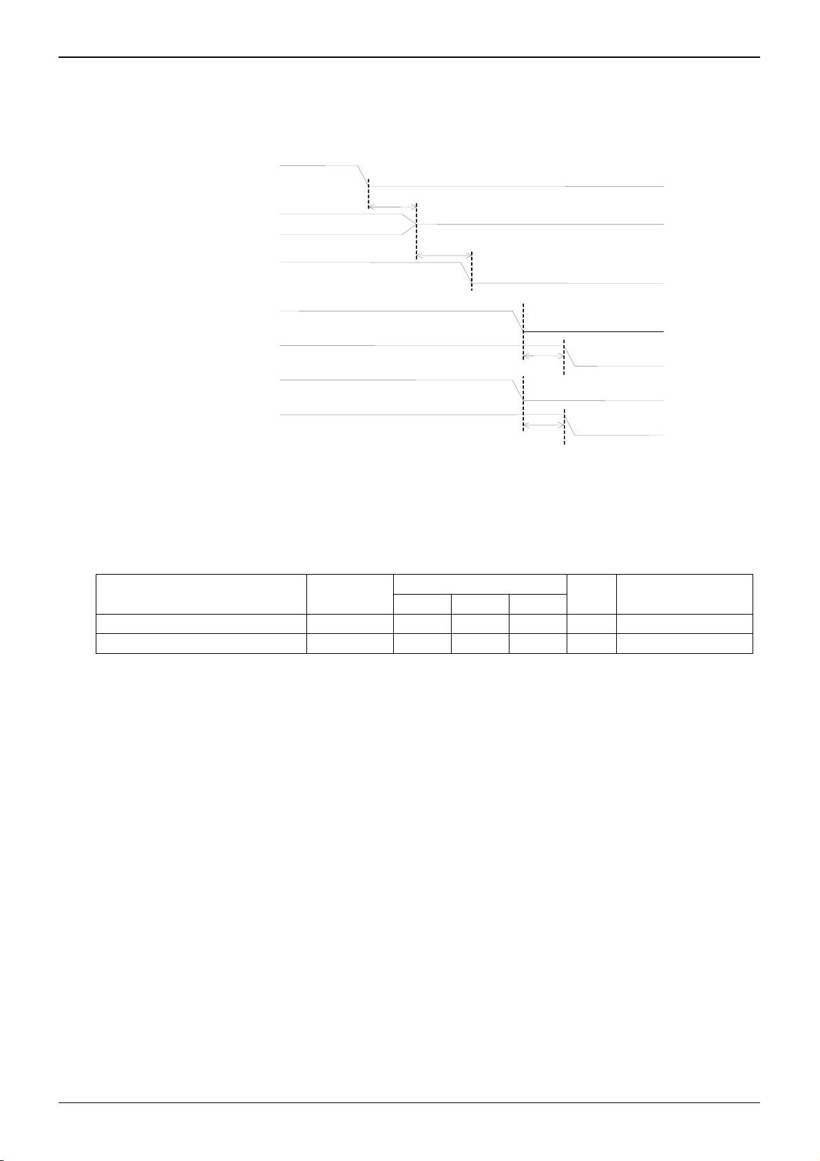
3) Power-On / Off Sequence
Power-On Sequence
Fig.10 shows power-on sequence of BU7964GUW.
Technical Note
DVDD , MSVDD of Tx
TX
t
SD
XSD of Tx
TX_IN
AL
t
PCLK of Tx
Tx MSDL 3 Output
DVDD , MSVDD of Rx
Stopped
HiZ
TX_OUT
t
RX
t
SD
XSD of Rx
RX_IN
AL
t
Rx Power mode
Rx All Outputs
Shutdown
Initial Value
Fig.10. Power-On Sequence
Table 13. Power-On Sequence Timing
Ta=25°C, DVDD=MSVDD=1.80V and DGND=MSGND=0.00V, unless otherwise noted.
Parameter Symbol
Min Typ Max
Provided
AL
Valid
/ Active
Standb
RX_OUT
t
AL
Valid Outputs
Tx : BU 7963 GUW
Rx: BU 7964 GUW
Limits Unit
Conditions
Reset Valid After Power Supplied t
PCLK Valid After XSD Released t
Parallel Data Valid After TX HighSpeed Signals Valid
RX_VDD_XSD
RX_IN_VAL
t
RX_OUT_VAL
10 - - µs
- - 10 µs
- - 2 ms
www.rohm.com
© 2010 ROHM Co., Ltd. All rights reserved.
12/18
2010.04 - Rev.A
BU7964GUW
_
XSD_
V
_
XSD_
V
Power-Off Sequence
Fig.11 shows the power-off sequence of BU7964GUW.
PCLK of Tx
Tx MSDL 3 Output
Rx All Outputs
XSD of Tx
Provided
Valid
Valid Outputs
TX_OUT_INV
t
Stopped
RX_OUT_INV
t
Technical Note
HiZ
Initial Value
DVDD , MSVDD of Tx
XSD of Rx
DVDD , MSVDD of Rx
Fig.11. Power-Off Sequence Timing
Table 14. Power-Off Sequence Timing
Ta=25°C, DVDD=MSVDD=1.80V, DGND=MSGND=0.00V, unless otherwise noted.
Parameter Symbol
Parallel output delay time t
XSD hold time t
RX_OUT_INV
RX_XSD_VDD
TX
RX
DD
DD
Tx : BU 7963 GUW
Rx: BU 7964 GUW
t
t
Limits
Min Typ Max
Unit Conditions
- - 100 µs
10 - - µs
www.rohm.com
© 2010 ROHM Co., Ltd. All rights reserved.
13/18
2010.04 - Rev.A

BU7964GUW
_
XSD_
_
XSD_
_
X
_
X
_
X
_
XSD_
●Frequency Change Sequence
Fig.12 shows the frequency change sequence of BU7964GUW.
DVDD , MSVDD
of Tx and Rx
TX
XSD of Tx
t
OUT
t
TX_IN
Technical Note
SD
PCLK of Tx
PLL _BW[ 1 : 0] of Tx
Frequency 1 Frequency 2
TX
t
State1
XSD of Rx
RX
t
PLL_BW[ 1 : 0] of Rx
State 1 State 2
Fig.12. Frequency Change Sequence
Table 15. Frequency Change Sequence Timing
Ta=25°C, DVDD=MSVDD=1.80V and DGND=MSGND=0.00V, unless otherwise noted.
Parameter Symbol
Control Signal Hold Time t
Control Signal Setup Time t
RX_XSD_CTL
RX_CTL_XSD
2.0 - - µs
2.0 - - µs
CTL
CTL
TX_CTL
t
RX_CTL
t
SD
SD
Limits
Min Typ Max
State 2
Tx : BU 7963 GUW
Rx: BU 7964 GUW
Unit Conditions
www.rohm.com
© 2010 ROHM Co., Ltd. All rights reserved.
14/18
2010.04 - Rev.A
BU7964GUW
●High-Speed Channel Characteristic
Table 16. High-speed channel characteristic
Ta=25°C, DVDD=MSVDD=1.80V and DGND=MSGND=0.00V, unless otherwise noted.
Parameter Symbol
Differential Voltage Range V
LOW-level threshold voltage V
HIGH-level threshold voltage V
Common Mode Voltage Range V
Internal termination resistance R
Operating Frequency f
RX sink current I
Link detection threshold voltage V
PULL_RX
LINK_RX
70 100 200 mVpp
diff_rx
-40 - - mV
thl
- - 40 mV
thh
0.6 0.9 1.2 V
cm_rx
75 100 125 Ω
_rx
- - 225 MHz
opr_rx
Min Typ Max
12 30 90 µA
0.2 0.3 0.4 V
Limits
Technical Note
Unit Conditions
fopr_rx
InP(D0+,D1+,D2+)
InN(D0-,D1-,D2-)
Differential
(InP-InN)
Differential
(InP-InN)
Single-end
Vcm_rx
Vdiff_rx
0
Vthh
0
Vthl
Fig.13. High-Speed Channel Characteristic
Fig.14 shows high-speed channel equivalent schematic.
www.rohm.com
© 2010 ROHM Co., Ltd. All rights reserved.
15/18
2010.04 - Rev.A

BU7964GUW
MSDL 3 TX
Logical input
to
MSDL 3 TX
MSVDD
MSGND
line
Transmission
VO +
I
LEA_T
I
LEA_R
RT/2
R
/2
R
RT/2
RR/2
VO -
I
LEA_T
I
LEA_R
I
MSGND
Fig.14. High-Speed Channel Equivalent Schematic.
MSDL 3 RX
MSVDD
VI+
VI-
MSGND
PUL_R
V
LIN_R
V
C
Technical Note
Logical output
from
MSDL 3 RX
MSVDD
Link detection
comparator
output
MSGND
www.rohm.com
© 2010 ROHM Co., Ltd. All rights reserved.
16/18
2010.04 - Rev.A
BU7964GUW
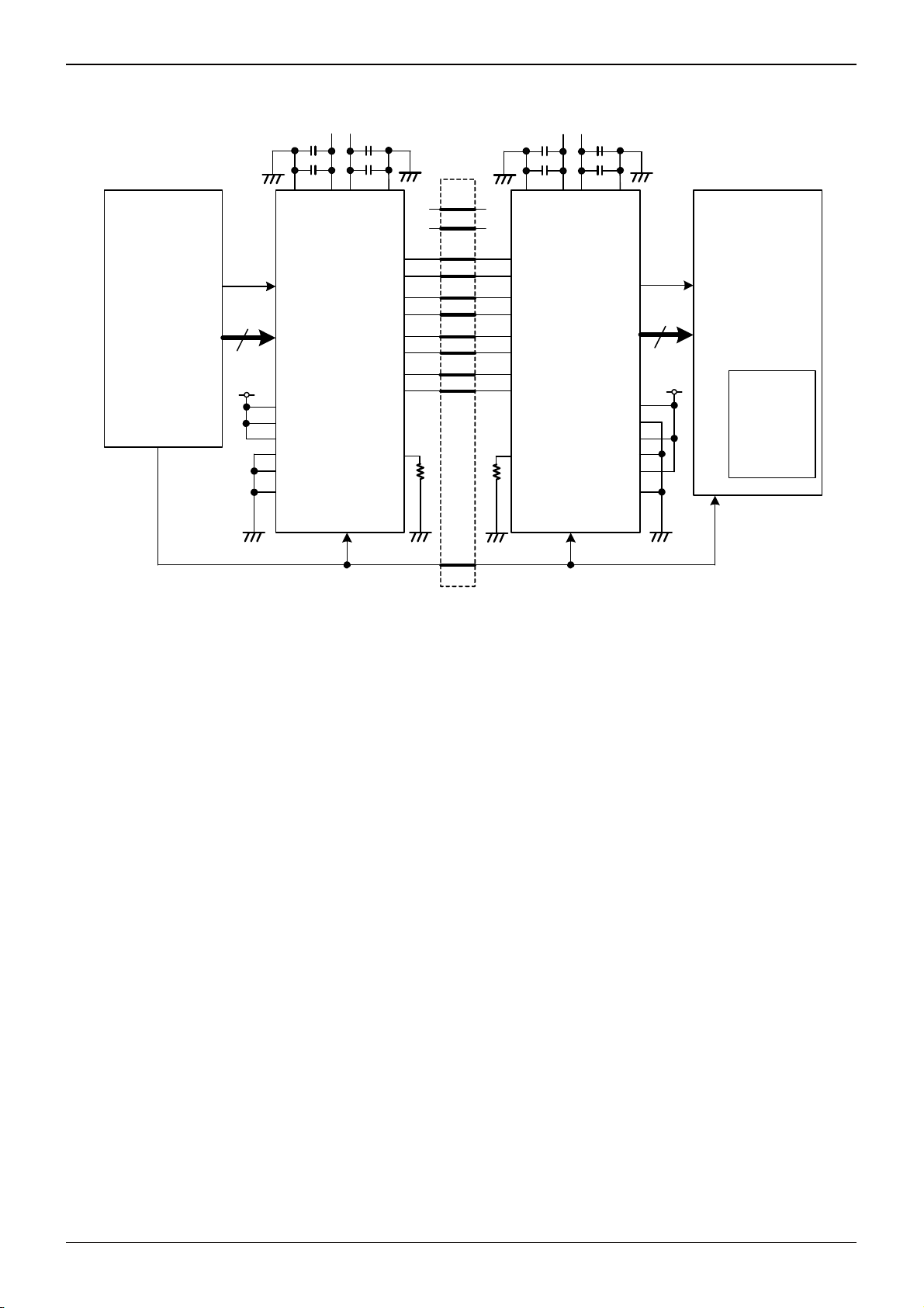
●Application Circuit Example
0.1μ×3
100p×3
1.8V
1.8V
0.1μ×2
100p×2
0.1μ×2
100p×2
1.8V
1.8V
100p×3
Technical Note
0.1μ×3
MPU
Pixel clock
R[7:0],G[7:0],B[7:0],
HS,VS,DE
Reset
1.8V
DVDD
DGND
MSVDD
MSGND
GND
CLK+
PCLK
27
PD[26:0]
CLK-
D0+
D0-
D1+
D1-
CKD CPO
DVDD
D2+
(Tx device)
BU7963GUW
D2-
1.8V
GND
MSGND
CLK+
CLK-
D0+
D0-
D1+
D1-
D2+
D2-
PLLBW
POL_PCLK
LS1
LS0
DRVR
DRVR
RVS
TEST[1:0]
10KΩ±5%
10KΩ±5%
XSD
DGND
MSGND
MSGND
Fig.15. Application Circuit
MSVDD
(Rx device)
BU7964GUW
TEST[1:0]
XSD
DVDD
PCLK
PD[26:0]
PLLBW1
PLLBW0
LS1
LS0
F_XS
DGND
27
DGND
Video Mode
LCD Controller
Pixel clock
R[7:0],G[7:0],B[7:0],
HS,VS,DE
DVDD
WVGA
LCD panel
Reset
www.rohm.com
© 2010 ROHM Co., Ltd. All rights reserved.
17/18
2010.04 - Rev.A
BU7964GUW
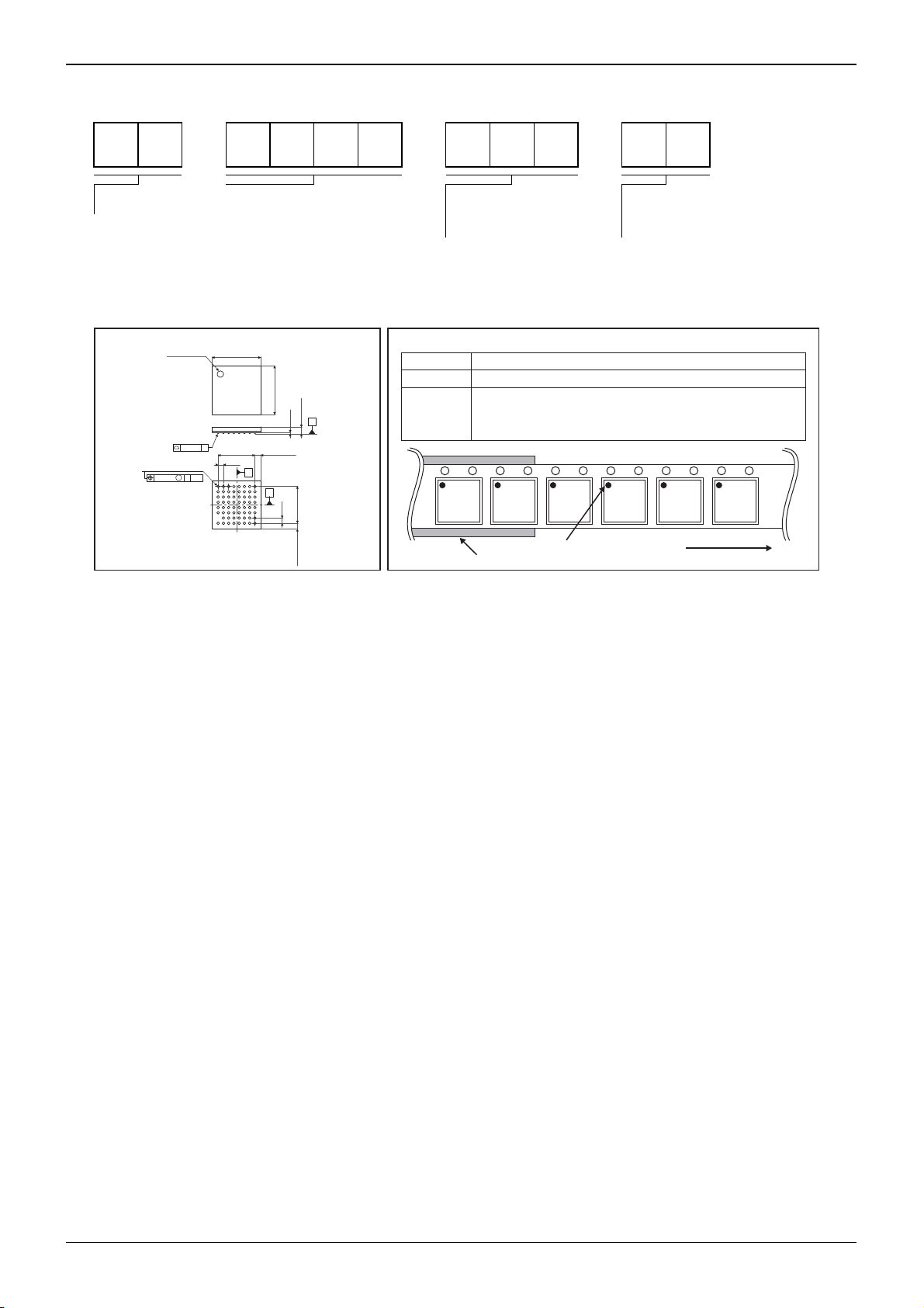
●Ordering Part Number
B U 7 9 6 4 G U W - E 2
Technical Note
Part No. Part No. Package
VBGA063W050
1PIN MARK
5.0±0.1
0.08 S
63-φ0.295±0.05
M
φ
0.05
P=0.5×7
ABS
H
G
F
E
D
C
B
A
5.0± 0.1
0.1
S
0.9MAX
0.75±0.1
0.5
A
B
0.5
3
762
4
51
P=0.5×7
8
0.75±0.1
(Unit : mm)
<Tape and Reel information>
Quantity
Direction
of feed
Packaging and forming specification
GUW: VBGA063W050
Embossed carrier tape (with dry pack)Tape
2500pcs
E2
The direction is the 1pin of product is at the upper left when you hold
()
reel on the left hand and you pull out the tape on the right hand
Reel
1pin
Order quantity needs to be multiple of the minimum quantity.
∗
E2: Embossed tape and reel
Direction of feed
www.rohm.com
© 2010 ROHM Co., Ltd. All rights reserved.
18/18
2010.04 - Rev.A

Notes
No copying or reproduction of this document, in part or in whole, is permitted without the
consent of ROHM Co.,Ltd.
The content specied herein is subject to change for improvement without notice.
The content specied herein is for the purpose of introducing ROHM's products (hereinafter
"Products"). If you wish to use any such Product, please be sure to refer to the specications,
which can be obtained from ROHM upon request.
Examples of application circuits, circuit constants and any other information contained herein
illustrate the standard usage and operations of the Products. The peripheral conditions must
be taken into account when designing circuits for mass production.
Great care was taken in ensuring the accuracy of the information specied in this document.
However, should you incur any damage arising from any inaccuracy or misprint of such
information, ROHM shall bear no responsibility for such damage.
The technical information specied herein is intended only to show the typical functions of and
examples of application circuits for the Products. ROHM does not grant you, explicitly or
implicitly, any license to use or exercise intellectual property or other rights held by ROHM and
other parties. ROHM shall bear no responsibility whatsoever for any dispute arising from the
use of such technical information.
Notice
The Products specied in this document are intended to be used with general-use electronic
equipment or devices (such as audio visual equipment, ofce-automation equipment, communication devices, electronic appliances and amusement devices).
The Products specied in this document are not designed to be radiation tolerant.
While ROHM always makes effor ts to enhance the quality and reliability of its Products, a
Product may fail or malfunction for a variety of reasons.
Please be sure to implement in your equipment using the Products safety measures to guard
against the possibility of physical injury, re or any other damage caused in the event of the
failure of any Product, such as derating, redundancy, re control and fail-safe designs. ROHM
shall bear no responsibility whatsoever for your use of any Product outside of the prescribed
scope or not in accordance with the instruction manual.
The Products are not designed or manufactured to be used with any equipment, device or
system which requires an extremely high level of reliability the failure or malfunction of which
may result in a direct threat to human life or create a risk of human injury (such as a medical
instrument, transportation equipment, aerospace machinery, nuclear-reactor controller, fuelcontroller or other safety device). ROHM shall bear no responsibility in any way for use of any
of the Products for the above special purposes. If a Product is intended to be used for any
such special purpose, please contact a ROHM sales representative before purchasing.
If you intend to export or ship overseas any Product or technology specied herein that may
be controlled under the Foreign Exchange and the Foreign Trade Law, you will be required to
obtain a license or permit under the Law.
Thank you for your accessing to ROHM product informations.
More detail product informations and catalogs are available, please contact us.
ROHM Customer Support System
www.rohm.com
© 2010 ROHM Co., Ltd. All rights reserved.
http://www.rohm.com/contact/
R1010
A
 Loading...