ROHM BU7961GUW Technical data

1/4
r
STRUCTURE
PRODUCTNAME
FUNCTION
Silicon Monolithic Integrated Circuit
BU7961GUW
Serial Interface for Mobile Devices Application
MSDL3(Mobile Shrink Data Link 3)
Serializer LSI
FEATURES
·Maximum transmission rate of highspeed differential interface MSDL3 is 900Mbps.
·Support LCD interface with 24bit parallel RGB video mode.
·Pixel clock frequency is 4~30MHz
.
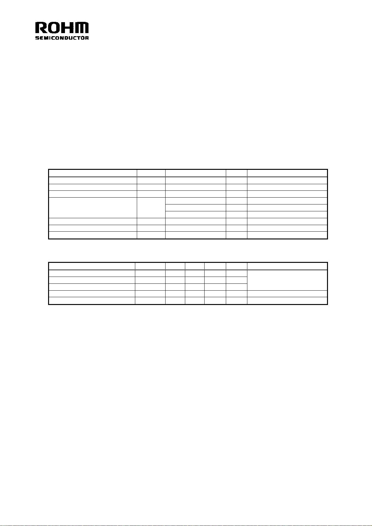
Absolute maximum
1.
Parameter Symbol Rated values Unit Remarks
Power supply voltage for IOVDD IOVDD -0.3 ~ +4.5 V
Power supply voltage for DVDD DVDD -0.3 ~ +2.5 V
Power supply voltage for MSVDD MSVDD -0.3 ~ +2.5 V
-0.3 ~ IOVDD+0.3 V I/O terminals of IOVDD line
Input voltage VIN
Input current IIN -10 ~ +10 mA
Package power dissipation Pd 300 * mW Without board mounted
Preservation temperature Tstg -55 ~ +125
*
When it uses by Ta=25oC or higher, reduce by 3.0 mW/°C (for a single package).
-0.3 ~ +3.6 V XSD terminal
-0.3 ~ MSVDD+0.3 V I/O terminals of MSVDD line
°C
Operating Condition
2.
Paramete
Supply voltage for IOVDD VIOVDD 1.65 1.80 3.60 V
Supply voltage for DVDD VDVDD 1.65 1.80 1.95 V
Supply voltage for MSVDD VMSVDD 1.65 1.80 1.95 V
PCLK frequency fPCLK 4.0 - 30.0 MHz
Operating temperature range Topr -30 25 +85
These goods are specific machines. Because the exclusive goods which are specially designed for the device are
considered. Whether that machine, device corresponds to strategic goods to decide as the foreign exchange and foreign
trade control law. You must have it judged.
As for contents of mention of these materials. A service in the foreign exchange and foreign trade control law
(Technology in the design, the manufacture and the use). Be careful of handling because it is likely to correspond.
This product is not designed against radioactive ray.
Symbol Min Typ Max Unit Remarks
VDVDD=VMSVDD≤VIOVDD
°C
REV. A

2/4
r
3.
ELECTRICAL CHARACTERISTICS
3.1 CMOS INOUT CHARACTERISTICS
Ta =2 5℃, DVDD=MSVDD=1.80V, IOVDD=1.80V, DGND=MSGND=0.00V, unless otherwise noted
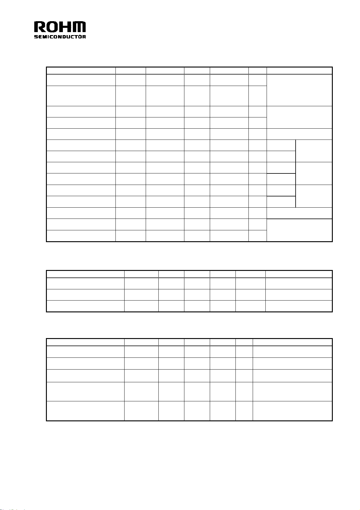
Parameter Symbol Min Typ Max Unit Conditions
‘L’ input voltage1 VIL1 DGND - 0.3*IOVDD V
‘H’ input voltage1 VIH1 0.7*IOVDD - IOVDD V
‘L’ input voltage2 VIL2 MSGND - 0.3*MSVDD V
‘H’ input voltage2 VIH2 0.7*MSVDD - MSVDD V
‘H’ input voltage3 VIH3 0.7*IOVDD - 3.6 V XSD terminal
PCLK, PD[26:0],
POL_PCLK,
PLL_BW[1:0],
LS0, RVS, TEST3
terminals
LS1 terminal
‘L’ output voltage1 VOL1 DGND - 0.3*IOVDD V IO=1mA
‘H’ output voltage1 VOH1 0.7*IOVDD - IOVDD V IO=-1mA
‘L’ output voltage2 VOL2 MSGND - 0.3*MSVDD V IO=1mA
‘H’ output voltage2 VOH2 0.7*MSVDD - MSVDD V IO=-1mA
PCLK frequency1 fPCLK1 4.0 - 15.0 MHz LS0=L
PCLK frequency2 fPCLK2 8.0 - 30.0 MHz LS0=H
PCLK duty cycle DPCLKI 33 - 67 % PCLK terminal
Data setup to PCLK tDSI 5.0 - - ns
Data hold to PCLK tDHI 5.0 - - ns
PD[26:0] terminals
3.2 MSDL3 TX CHARACTERISTICS
Ta =2 5℃, DVDD=MSVDD=1.80V, IOVDD=1.80V, DGND=MSGND=0.00V, unless otherwise noted
Parameter Symbol Min Typ Max Unit Conditions
Differential voltage range Vdiff_tx 100 150 200 mVpp
Common mode voltage range Vcm_tx 0.8 0.9 1.0 V
SubLVDS data rate DR_tx 120 - 450 Mbps/ch
3.3 CURRENT COMSUMPTION
Ta =2 5℃, DVDD=MSVDD=1.80V, IOVDD=1.80V, DGND=MSGND=0.00V, unless otherwise noted
Paramete
Shutdown current Iop_sht_tx - 0.2 10.0 μA XSD=L, PCLK=L
Symbol Min Typ Max Unit Conditions
CKD
terminal
LS_EN
terminal
PCLK
terminal
Standby current Iop_stb_tx - 0.2 10.0 μA XSD=H, PCLK=L
Active current of
1ch27bit format
Active current of
2ch27bit format
Active current of
1ch13bit format
*1 : Total operating current(IDVDD+IMSVDD+IIOVDD) with PD[26:0] inputs toggling 0x2AAAAAA and 0x5555555.
*2 : Total operating current(IDVDD+IMSVDD+IIOVDD) with PD[26:15],PD[2] inputs toggling 0x0AAA and 0x1555.
Iop_act_tx1 - 14.0 18.5 mA
Iop_act_tx2 - 19.7 25.7 mA
Iop_act_tx3 - 16.3 21.3 mA
REV. A
LS[1:0]=LL, PLL_BW[1:0]=HL,
fPCLK=15MHz, *1
LS[1:0]=LH,
PLL_BW[1:0]=HL,
fPCLK=30MHz, *1
LS[1:0]=HH,
PLL_BW[1:0]=HL,
fPCLK=30MHz, *2
 Loading...