


A
Audio Accessory ICs for Mobile Devices
Mixer & Selector ICs
with 16bit D/A Converter
BU7858KN,BU7893GU
●Description
This LSI is mounted with stereo 16bit D/A Converter and suitable for higher sound quality and miniaturization of cellular
phone with music play. BU7893GU has a 3D surround enhancement function and hence can play the wide-spreading
stereo sound from stereo speakers that are arranged nearby.
●Features
1) Mounted with Stereo 16bit audio D/A converter
2) Compatible with Stereo analogue interface
3) Stereo headphone amplifier (16Ω)
4) Low-band corrective circuit in headphone amplifier
5) Volume that can adjust the gain
6) Flexible mixing function
●Applications
Portable information & communication equipments such as cellular phone and PDA (Personal Digital Assistant) etc.
Cellular phone with music play
●Line up matrix
Function BU7858KN BU7893GU
No.10087EAT03
Stereo audio D/A converter 16bit 16bit
16bit Right justified
Stereo audio interface format
3D surround enhancement function No Yes
3 band equalizer No Yes
Stereo headphone amplifier 16Ω driver 16Ω driver
Line output (600Ω driver) Yes No
Headphone amplifier low-band correction function Built-in Built-in
Click noise reduction function
Package VQFN28 VCSP85H3
18bit Right justified
IIS
Yes
(headphone only)
16bit Left justified
16bit Right justified
IIS
Yes
www.rohm.com
1/24
© 2010 ROHM Co., Ltd. All rights reserved.
2010.09 - Rev.
A
BU7858KN,BU7893GU
●Absolute maximum ratings
Parameter Symbol Ratings Unit
Technical Note
BU7858KN VDD -0.3 ~ 4.5 V
Power-Supply Voltage
BU7893GU
DVDDIO
AVD D
-0.3 ~ 4.5
DVDDCO -0.3 ~ 2.5
*1
580
*2
Power Dissipation
Operating Temperature
BU7858KN
Pd
BU7893GU 700
BU7858KN
T
OPR
-20 ~ +85
BU7893GU -30 ~ +85
Storage Temperature
BU7858KN
T
STG
-55 ~ +125
BU7893GU -50 ~ +125
*1 : 5.8mW is decreased every 1℃ when using it over 25℃. (Mounted on the ROHM standard PCB )
*2: 7.0mW is decreased every 1℃ when using it over 25℃.
●Operating conditions
【BU7858KN】
Parameter Symbol
Min. Typ. Max.
Ratings
Power-Supply Voltage VDD 2.7 3.0 3.3 V
【BU7893GU】
Parameter Symbol
Min. Typ. Max.
Ratings
V
mW
℃
℃
Unit
Unit
Analog Power-Supply Voltage AVDD 2.6 2.8 3.3 V
Digital I/O Power-Supply Voltage DVDDIO DVDDCO 1.8 3.3 V
Digital Core Power-Supply Voltage DVDDCO 1.62 1.8 1.98 V
www.rohm.com
2/24
© 2010 ROHM Co., Ltd. All rights reserved.
2010.09 - Rev.

A
BU7858KN,BU7893GU
●Electrical characteristics
【BU7858KN】
Unless otherwise specified, Ta=25℃, AVDD=DVDD=3.0V
・Analog
Parameter Symbol
Min. Typ. Max.
Limits
Unit Conditions
Current Consumption Idd3 - 2.3 3.7 mA 16Ω driver part and no signal
Technical Note
DAC S/(N+D) SN+D - 85 - dB
DAC S/N SNR - 92 - dB
Headphone Amplifier
Total Harmonic Distortion
Headphone Amplifier
Maximum Output
Headphone Amplifier
Output Noise Voltage
THDhp - 0.05 0.5 %
PO - 10 - mW fin=1kHz, THD=10%, RL=16Ω
VNO - -94 -80 dBV A-weighted
SPO Maximum Output Level VOMAX1 2.0 - - V
EXTO Maximum Output Level VOMAX2 2.0 - - V
fs=44.1kHz, fin=1kHz, 20kHz
LPF, Vin=-0.5dBFS
fs=44.1kHz, fin=1kHz
, A-weighted, Vin=0dBFS
fin=1kHz, 20kHz LPF,
Vin=-10dBV
fin=1kHz, THD≦1%, 10kΩLoad
P-P
fin=1kHz, THD≦1%, 600ΩLoad
P-P
・Digital (DC)
Parameter Symbol
Min. Typ. Max.
Digital Input Voltage “L” VIL - -
Digital Input Voltage “H” VIH
0.8 x
DVDD
Limits
0.2 x
DVDD
Unit Conditions
V
- - V
Digital Output Voltage “L” VOL - - 0.5 V Iol=-500µA
Digital Output Voltage “H” VOH
DVDD
-0.5
- - V Ioh=500µA
Input Leakage Current 1 IIN1 - - ±2 µA at 0V, 3V
・Audio Interface
Parameter Symbol
Min. Typ. Max.
Limits
Unit Conditions
MCLKI Frequency fMCLK 4.096 - 18.432 MHz
MCLKI Duty Ratio dMCLK 45 - 55 %
LRCLK Frequency fs 16 - 48 kHz
LRCLK Duty Ratio dLR 45 - 55 %
BCLK Frequency fBCK 0.512 - 3.072 MHz
BCLK Duty Ratio dBCK 45 - 55 %
LRCLK edge to BCLK↑ Time tLRS 50 - - ns
BCLK↑ to LRCLK Edge Time tSLR 50 - - ns
Data Hold Time tSDH 50 - - ns
Data Set-up Time tSDS 50 - - ns
www.rohm.com
3/24
© 2010 ROHM Co., Ltd. All rights reserved.
2010.09 - Rev.

A
BU7858KN,BU7893GU
Technical Note
【BU7893GU】
・Whole Block
Unless otherwise specified, Ta=25℃, DVDD_CORE=1.8V, DVDD_IO=1.8V, AVDD=2.8V, Digital input terminal is fixed
with DVDD_IO “L” or “H” level, The gain settings of the audio paths are all 0dB, and no signal
Parameter Symbol
DVDD_CORE Stand-by Current
(Core logic block)
Min. Typ. Max.
ISTCO - - 10 µA standby,CLKI = DVSS
Limits
Unit Conditions
DVDD_IO Stand-by Current ISTIO - - 5 µA standby,CLKI = DVSS
AVDD Stand-by Current ISTA - - 5 µA standby
DVDD_CORE Operation Current IDDCO - 5 10 mA
DVDD_IO Operation Current IDDIO - 0.1 1 mA
AVDD Operation Current 1
(Analog melody)
AVDD Operation Current 2
(Digital melody)
IDDA1 - 1.6 2.8 mA
IDDA2 - 6.0 10.0 mA
BCLK,LRCLK = Input mode
MCLK = L output
ANAINL→MIX1→SPOL
ANAINR→MIX2→SPOR
SDI→MIX1→SPOL
SDI→MIX2→SPOR
TCXOI = 19.8MHz,fs = 44.1kHz
・DC Characteristic
Parameter Symbol Terminal
L Output Voltage
H Output Voltage
L Level Input Voltage1
L Level Input Voltage 2 CLKI
H Level Input Voltage 1
H Level Input Voltage 2 CLKI
L Level Input Current
H Level Input Current 1
H Level Input Current 2 CLKI
Output OFF Current
※1 : They also contain interactive terminals that are set output state.
※2 : They also contain interactive terminals that are set input state.
※3 : Please connect 100pF coupling capacitor and input 0.5V
(In address 15h CLKSEL1=0, CLKSEL0=1)
※4 : At interactive terminals of input state or three-state terminals of output-disable state
All output
terminal
All output
terminal
All input
terminal
All input
terminal
All input
terminal
All input
terminal
Hi-Z
terminal
※
※
※
3
※
Vild2 -0.3
※
3
※
Vihd2
※
※
3
※
Iihd2 -1 1 µA
※
Vold 0 0.30 V Iol=+0.8mA
1
Vohd
1
Vild1 -0.3 DVSS+0.5 V
2
Vihd1
2
Iild -1 1 µA
2
Iihd1 -1 1 µA
2
Iozd -10 10 µA
4
DVDD_IO
-0.30
DVDD_IO
or more when you input through coupling capacitor.
P-P
Limits
Min. Max.
Unit Conditions
DVDD_IO V Ioh=-0.8mA
3
-0.5
3
※
※
DVDD_IO
+0.3
DVDD_CORE
+0.3
V
V
V
Input terminal voltage is
DVSS
Input terminal voltage is
DVDD_IO
Input terminal voltage is
DVDD_CORE
・Audio Path(MIX)
Unless otherwise specified, Ta=25℃, AVDD=2.8V, reference input level=-6dBV, f=1kHz, A-weighted, path gain =0dB
Limits
Parameter Symbol
Unit Conditions
Min. Typ. Max.
ANAL_V Volume Setting G
ANAR_V Volume Setting G
-11 - +3 dB 1dB step
DACL
-11 - +3 dB 1dB step
DACR
www.rohm.com
4/24
© 2010 ROHM Co., Ltd. All rights reserved.
2010.09 - Rev.
A
BU7858KN,BU7893GU
Technical Note
・Audio Path (SP PREamp)
Unless otherwise specified,Ta=25℃,AVDD=2.8V, Reference input level =-6dBV, f=1kHz,
A-weighted, path gain =0dB, RL=33kΩ
Parameter Symbol
Min. Typ. Max.
Limits
Unit Conditions
THD+N THDSP - -70 -60 dB 20kHz LPF
Output Noise Voltage V
- -90 -80 dBV At no a signal
NOSP
Mute Level MLSP - -90 -80 dB 1kHz BPF
・Audio Path (HP amp)
Unless otherwise specified, Ta=25℃, AVDD=2.8V, reference input level =-6dBV, f=1kHz,
A-weighted, path gain =0dB, RL=16Ω
Parameter Symbol
Min. Typ. Max.
Limits
Unit Conditions
THD+N THDHP - -65 -55 dB 20kHz LPF
Output Noise Voltage V
The Maximum Output Power P
- -90 -80 dBV At no signal
NOHP
10 - - mW THD=10%,16Ω load
OHP
Channel Separation CSHP - -80 -70 dB Vo=-14dBV,1kHz BPF
Mute Level MLHP - -90 -80 dB 1kHz BPF
HPL_V Volume Setting 1 GA1
HPL_V Volume Setting 2 GA2
HPR_V Volume Setting 1 GA1
HPR_V Volume Setting 2 GA2
-48 - 0 dB 2dB step
HPL
-42 - +6 dB 2dB step
HPL
-48 - 0 dB 2dB step
HPR
-42 - +6 dB 2dB step
HPR
・3D Surround, Equalizer, and Audio DAC
Unless otherwise specified, Ta=25℃, AVDD=2.8V, BCLK=64fs, LRCLK=256fs, f=1kHz, path gain=0dB,
SPOL/SPOR output, SPOL/SPOR= no load, output=0dBFS
Parameter Symbol
Min. Typ. Max.
Full-scale Amplitude VMAX 1.40 1.68 2.00 V
S/N1 (A-Weighted) DAC
70 75 - dB
sn1
Limits
Unit Conditions
0.6×AVDD
P-P
THD+N1 (20kHz LPF) DACthd1 - -70 -60 dB fs=8,11.025kHz
THD+N2 (20kHz LPF) DACthd2 - -75 -65 dB fs=16,22.05,32,44.1,48kHz
・Audio I/F Format
Unless otherwise specified, Ta=25℃, DVDD_IO=1.62~3.3V, DVDD_CORE=1.62~1.98V
Parameter Symbol
Min. Typ. Max.
Limits
Unit Conditions
BCLK Output Frequency FBCKO 0.512 - 3.072 MHz 64fs
LRCLK Output Frequency FLRCKO 8 - 48 kHz
SDI Set-up Time tSDSU 100 - - nsec
SDI Hold Time tSDH 100 - - nsec
・PLL
Unless otherwise specified, Ta=25℃, AVDD=2.8V, BCLK = no load
Parameter Symbol
Min. Typ. Max.
Limits
Unit Conditions
PLL Lock-up Time Tlock1 - - 10 msec
PLL Jitter Tjitter1 - 200 - psec BCLK terminal,f
=65.536MHz
VCO
www.rohm.com
5/24
© 2010 ROHM Co., Ltd. All rights reserved.
2010.09 - Rev.

A
BU7858KN,BU7893GU
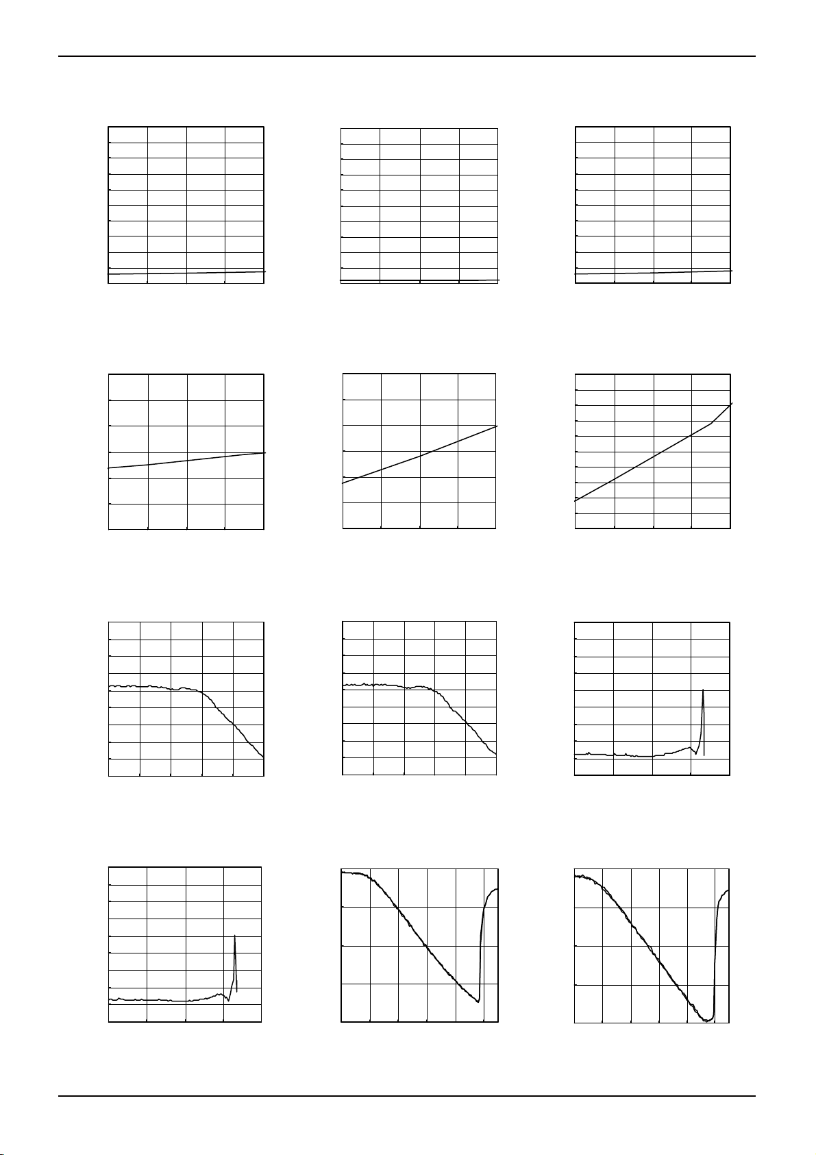
●Reference Data
【BU7858KN】
10.0
A)
μ
8.0
6.0
4.0
2.0
STAND BY CURRENT : ICC (
0.0
2.0 2.5 3.0 3.5 4.0 4.5
SUPLLY VOLTAGE : VD D( V)
Fig.1 Stand-by Current
-30
-40
-50
-60
-70
-80
THD+N ( dB)
-90
-100
-110
-120
-110 - 90 -70 - 50 -30 - 10
IN PUT LEVEL : VIN (dB FS)
Fig.4 16bit D/A Converter Total
Harmonic Distortion (Lch)
-30
-40
-50
-60
-70
-80
THD+N (dB)
-90
-100
-110
-120
10 100 1000 10000 100000
INPUT SIGNAL Fr eq : F IN( Hz)
Fig.7 16
bit D/A Converter
Total Harmonic Distortion (Rch)
100.00
10.00
1.00
THD+N (%)
0.10
0.01
-100 - 80 - 60 -40 - 20 0
INPU T LEVEL : VIN(dBV)
Fig.10 SPO
Total Harmonic Distortion
14.0
12.0
10.0
8.0
6.0
4.0
2.0
CIRCUIT CURRENT : ICC (mA)
0.0
2.0 2.5 3.0 3.5 4.0 4.5
SUPLLY VOLTAGE : VD D( V)
Fig.2 16bit D/A Converter
Operation Current
-30
-40
-50
-60
-70
-80
THD+N (dB)
-90
-100
-110
-120
-110 - 90 -70 - 50 - 30 - 10
INPU T LEVEL : VIN( dBFS)
Fig.5 16bit D/A Converter
Total Harmonic Distortion (Rch)
100.00
10.00
1.00
THD+N (%)
0.10
0.01
-100 - 80 -60 -40 - 20 0
IN PUT LEVEL : VIN (dBV)
Fig.8 Headphone Amplifier
Total Harmonic Distortion (HP_L)
100.00
10.00
1.00
THD+N (%)
0.10
0.01
-100 - 80 -60 - 40 -20 0
INPUT LEVEL : VIN (dB V)
Fig.11 EXTO
Total Harmonic Distortion
Technical Note
6.0
5.0
4.0
3.0
2.0
1.0
CIRCUIT CURRENT : ICC (mA)
0.0
2.0 2.5 3.0 3.5 4.0 4.5
SUPLLY VOLTAGE : VD D( V)
Fig.3 Headphone Amplifier
Operation Current
-3 0
-4 0
-5 0
-6 0
-7 0
-8 0
THD+N (dB)
-9 0
-100
-110
-120
10 100 1000 10000 100000
INPUT SIGNAL Freq : FIN(Hz)
Fig.6 16bit D/A Converter
Total Harmonic Distortion (Lch)
100.00
10.00
1.00
THD+N (%)
0.10
0.01
-100 - 80 -60 -40 - 20 0
INPUT LEVEL : VIN (dB V)
Fig.9 Headphone Amplifier
Total Harmonic Distortion (HP_R)
www.rohm.com
6/24
© 2010 ROHM Co., Ltd. All rights reserved.
2010.09 - Rev.
A
BU7858KN,BU7893GU
Technical Note
【BU7893GU】
5.0
4.5
A)
μ
4.0
3.5
3.0
2.5
2.0
1.5
1.0
STAND BY CURRENT : ICC (
0.5
0.0
1.6 1. 7 1.8 1.9 2.0
SUPLLY VOLTAGE : D VDD _COR E(V)
Fig.12 DVDD_CORE
Standby Current
5.0
4.5
A)
μ
4.0
3.5
3.0
2.5
2.0
1.5
1.0
STAND BY CURRENT : ICC (
0.5
0.0
2.6 2.8 3.0 3. 2 3.4
SUPLLY VOLT AGE : AVDD( V)
Fig.13 AVDD
Standby Current
5.0
4.5
A)
μ
4.0
3.5
3.0
2.5
2.0
1.5
1.0
0.5
CIRCUIT BY CURRENT : ICC (
0.0
1.6 1.7 1.8 1.9 2.0
SUPLLY VOLTAGE : DVDD_CORE(V)
Fig.14 DVDD_CORE
Operation Current (Analog melody)
2.0
1.9
1.8
1.7
1.6
1.5
CIRCUIT CURRENT : ICC (mA)
1.4
2.6 2. 8 3.0 3.2 3.4
SUPLLY VOLTAGE : AVDD (V)
Fig.15 AVDD
Operation Current (Analog melody)
5.0
4.5
4.0
3.5
3.0
2.5
CIRCUIT CURRENT : ICC (mA)
2.0
1.6 1.7 1.8 1.9 2.0
SUPLLY VOLT AGE : DVDD _CORE( V)
Fig.16 DVDD_CORE
Operation Current (digital melody)
4.0
3.9
3.8
3.7
3.6
3.5
3.4
3.3
3.2
CIRCUIT CURRENT : ICC (mA)
3.1
3.0
2.6 2. 8 3.0 3.2 3.4
SUPLLY VOLT AGE : AVDD( V)
Fig.17 AVDD
Operation Current (digital melody)
0.0
-10. 0
-20. 0
-30. 0
(dB)
-40. 0
-50. 0
THD+N
-60. 0
-70. 0
-80. 0
-90. 0
-100 - 80 -60 - 40 -20 0
INPU T LEVEL (dBF S)
Fig.18 16bit D/A Converter
Total Harmonic Distortion 1kHz (SPOL)
0.0
-10. 0
-20. 0
-30. 0
(dB)
-40. 0
-50. 0
THD+N
-60. 0
-70. 0
-80. 0
-90. 0
10 100 1000 10000 100000
INPUT SIGNAL FREQUENCY (Hz)
Fig.21 16bit D/A Converter
Total Harmonic Distortion (SPOR)
www.rohm.com
7/24
© 2010 ROHM Co., Ltd. All rights reserved.
0.0
-10.0
-20.0
-30.0
(dB)
-40.0
-50.0
THD+N
-60.0
-70.0
-80.0
-90.0
-100 - 80 - 60 -40 -20 0
INPU T LEVEL (dBFS)
ig.19 16bit D/A Converter
F
Total Harmonic Distortion 1kHz (SPOR)
100.00
10.00
(%)
1.00
THD+N
0.10
0.01
-100. 0 -80. 0 - 60.0 - 40.0 - 20.0 0.0
INPU T LEVEL (dBV)
Fig.22 Headphone Amplifier
Total Harmonic Distortion (HPOL / HPOR)
0.0
-10. 0
-20. 0
-30. 0
(dB)
-40. 0
-50. 0
THD+N
-60. 0
-70. 0
-80. 0
-90. 0
10 100 1000 10000 100000
INPU T SIGNA L FR EQU ENC Y (Hz )
Fig.20 16bit D/A Converter
Total Harmonic Distortion (SPOL)
100.0
10.0
(%)
1.0
THD+N
0.1
0.0
-100 - 80 -60 - 40 - 20 0
INPU T LEVEL (dBV)
Fig.23 Speaker Preamp
Total Harmonic Distortion (SPOL / SPOR)
2010.09 - Rev.

A
BU7858KN,BU7893GU
●Block diagram and pin assignment
【BU7858KN】
PLLC
MCLKO
PLL
RXI
RING
BCLK
MCLKI
BCLK
LRCLK
SDTI
MEL_R
MEL_L
EXTI
Digital
Audio
I/F
MEL_L
22
MEL_R
23
RING
24
RXI
25
PLLC
26
MCLKO
27
MCLKI
28
AVSSAVDDDVSSDVDD
MIX-
SEL1
SW1
+
ATT1
Digit
al
ATT
CVCOM
SW2
BIAS
16bit
DAC
16bit
DAC
LPF
LPF
ATT
ATT
NRST
Serial Control
SCLK
SDATA SCS
MIX-
SEL2
MIXSEL3
MIXSEL4
Fig.24 BU7858KN Block Diagram
21
EXTI
1
SDTI
SPO
20
2
LRCLK
19
EXTO
3
BCLK
AVDD
18
4
AVSS
HP_L
16
17
5
6
SCLK
DVSS
DVDD
Fig.25 BU7858KN Pin Assignment (TOP VIEW)
15
CA_L
7
ATT2
ATT3
ATT4
ATT5
SDATA
CSTEP
14
13
12
11
10
9
8
CSTART
CA_R
HP_R
CVCOM
CSTART
CSTEP
NRST
NCS
Technical Note
+
+
+
-
+
-
600Ω
16Ω
16Ω
SPO
EXTO
HP_R
CA_R
HP_L
CA_L
SP Amp
www.rohm.com
8/24
© 2010 ROHM Co., Ltd. All rights reserved.
2010.09 - Rev.

A
BU7858KN,BU7893GU
【BU7893GU】
0.1μF
CSTEP
Stereo Analog Interface
(From Melody LSI)
ANAINL
ANAINR
19.2MHz/
19.68MHz/
19.8MHz
CLKI
PLLC
Stereo PCM Interface
(MP3,AAC,etc)
MCLK
LRCLK
BCLK
SDI
1 2 3 4 5 6
1μF
PLL
DAI
VOL
VOL
CPOP
CPOP
Sonaptic
Serial I/F
SCLK
RSTB
Equalizer
3D
SIO
SO
SPI
DAC
DAC
CSB
-6dB
-6dB
-6dB
-6dB
COMOUT
VREF
+
+
Fig.26 BU7893GU Block diagram
1μF 1μF
COMIN
RX
EXT
DACL
DACR
RX
EXT
DACL
DACR
RX
EXT
DACL
DACR
RX
EXT
DACL
DACR
DVSS
DVDD_IO
DVDD_CORE
VOL
VOL
AVSS AVDD
Technical Note
CCL
HPOL
HPOR
CCR
SPOL
SP Amp
SPOR
SP Amp
6800p
6800p
8Ω
8Ω
100μ
+
100μ
+
16Ω
16Ω
A TEST3 HPOR HPOL CPOP SPOL TEST4
B CCR RSTB DVSS CCL SPOR COMIN
C SCLK SO
D SIO MCLK
CSTEP AVSS
COMOUT ANAINR
E CSB PLLC AVDD DVDD_CORE SDI ANAINL
F TEST2 CLKI DVDD_IO BCLK LRCLK TEST1
( TOP VIEW )
Fig.27 BU7893GU Ball Assignment
www.rohm.com
9/24
© 2010 ROHM Co., Ltd. All rights reserved.
2010.09 - Rev.

A
BU7858KN,BU7893GU
Technical Note
●Digital interface of 16 bit audio D/A converter
16bit audio D/A converter equipped with this series can be used with the following audio format.
【BU7858KN】
1) MSB first 16bit data (Right justified)
LRCLK(fs)
Lch
Rch
BCLK(64fs)
SDTI
0 1 2 15 14 13 12 11 4 3 2 0 1 Don’t Care Don’t Care
15
14
11 12 13
4
0 1 2 3
15:MSB, 0:LSB
2) MSB first 18bit data (Right justified)
LRCLK(fs)
Lch
Rch
BCLK(64fs)
17
SDTI
0 1 2 17 16 15 14 11 4 3 2 0 1 Don’t Care Don’t Care
16
11 14 15
4
0 1 2 3
17:MSB, 0:LSB
3) IIS mode 18bit data (Left justified)
LRCK(fs)
Lch
Rch
BCLK(64fs)
SDTI
Care
17 16 Don’t
4
2
3
Don’t Care
0 1
17
16
17:MSB, 0:LSB
4
3
0
2
1
Don’t Care
17 16
4) IIS mode 16bit data (BCLK=32fs)
LRCLK(fs)
Lch
Rch
BCLK(32fs)
15
14
12
13
SDTI
2
11
15:MSB, 0:LSB
0 1 2 3 6 7 8 9 10 0 1
0
2 3 6 7 8 9 10 15 14 13 12 11
15
1
14 13
Fig.28 AUDIO I/F FORMAT (BU7858KN)
BU7858KN is provided with a mode that generates MCLK (Master Clock) by using the built-in PLL, so it is possible to make
a D/A converter operate even if the clocks are only BCLK (64fs/32fs), LRCLK (fs).
The PLL generates MCLK (Master Clock), which is necessary for driving of D/A converter, from BCLK (Bit Clock).
Please connect a capacitor (PLLC) for the filter with DVSS. Moreover, please place the capacitor nearest DVSS of IC in
order to reduce the noise interference.
Then it is possible to monitor the master clock that is generated internally from MCLKO, which is after all the monitor
terminal, and hence does not guarantee drivability and phase-margin.
Please tie the MCLKI terminal to DVSS when PLL is used. And please tie the PLLC terminal to DVSS when PLL is not used.
Moreover, it is not necessary to set the “PLLPDN” and “SMPR” when PLL is not used.
www.rohm.com
10/24
© 2010 ROHM Co., Ltd. All rights reserved.
2010.09 - Rev.

A
BU7858KN,BU7893GU
【BU7893GU】
1. MSB first left justified format
Technical Note
LRCLK
BCLK
SDI
0 1 2 3 13 14 15 16 17 18 29 30 31 123 13
15 14 13 2 1 0 15 14 13 2 1 0
Don't care
Don't care Don't care Don't care
0
RchLch
14 15 16 17 18 29 30 31
0
15
2. MSB first right justified format
SDI
Don't care Don't careDon't care
15 14 13 2 1 0 2 1 015 14 13
Don't
care
3. IIS format
LRCLK
BCLK
SDI
0 1 2 3 4 141516171819 30 31 1 2 3 141516171819 30310 0
Don't
15 14 13 2 1 0
care
Don't care
Don't care Don't care
15 14 13 2 1 0
4
RchLch
Don't care
Fig.29 AUDIO I/F Format (BU7893GU)
●3D Surround enhancement function
【BU7893GU】
Even under the circumstances of adjacent arrangement of stereo speakers, the wide-spreading acoustic effect can be
achieved because of the output resulting from the digital audio input to which the 3D surround effect has been applied.
Moreover, the stereo sound at the time of audio recording can also be played truly. Please tell us about the parameter
setting when you use this function.
●Low-band corrective circuit
In the headphone output terminals (HP_L, HP_R or HPOL, HPOR), there is a low-band corrective circuit, which corrects the
low-band attenuation.
100kΩ
200kΩ
200kΩ
-
+
CHPx
C
HP_X
HPOX
CA_X
or
CCX
CL
+
or
OUTPUT
RL
Fig.30 BU7858KN & BU7893GU Headphone Output Equivalent Circuit
Low-band cut-off frequency fC= 1/(2・π・CL・RL)
Low-band boost frequency fBOOST = 1/(2・π・CCHPx・200kΩ)
Boost gain ABOOST = 20・log((200 kΩ+1/(2・π・f・CCHPx))/100 kΩ)
(the maximum low-band boost is 6dB)
For parameter setting, determine the output coupling capacitance CL and the headphone impedance R
before calculating
L
the low-band cut-off frequency fC. Then determine CCHPx so that the low-band cut-off frequency fC is roughly in
agreement with the low-band boost frequency fBOOST.
The recommended parameter setting of BU7858KN and BU7893GU is CCHPx = 6800pF at the time of CL = 100µF and
RL = 16Ω.
www.rohm.com
11/24
© 2010 ROHM Co., Ltd. All rights reserved.
2010.09 - Rev.

A
BU7858KN,BU7893GU
A
A
Technical Note
The frequency characteristic (theorical value) when the recommended constants are used is shown below.
10
5
0
-5
-10
-15
Gai n [ dB]
-20
-25
-30
-35
-40
1 10 100 1000 10000 100000
mplifier output
fter correction
Before correction
Fre quen cy [Hz]
Fig.31 Low-band corrective circuit Frequency characteristic
●CPU Interface
BU7858KN and BU7893GU can be controlled by using CPU interface.
【BU7858KN】
NCS
SCLK
SDATA
tcs
tds
A7
A6
tdh
A5
A4
tcyc
A3
A2
A1
A0
D7
D6 D5
D4 D3
D2 D1
tch
D0
Fig.32 CPU I/F Timing Chart 1 (BU7858KN)
After the falling edge of NCS, SDATA inputs are settled by 16 clock of SCLK, and data is written in the rising edge of NCS.
The data format is “16bit right justified”.
CPU interface is that 1Byte=16bit. It is absolutely necessary to insert the interval of NCS=”H” between first Byte and
Second Byte because it is not compatible with continuous data transmission. For the following th, please wait the time more
than 1 SCLK Clock. (th≧tcyc)
NCS
th
SCLK
SDATA
Fig.33 CPU I/F Timing Chart 2 (BU7858KN)
・AC Characteristics
Ta =2 5℃, AVDD=DVDD=3.0V
Parameter Symbol
SCLK Width
SDATA Input Hold Time
SDATA Input Set-up Time
NCS Set-up Time
NCS Hold Time
*It is recommended to use exclusive lines for CPU interface.
tcyc 250 - - ns
tdh 50 - - ns
tds 50 - - ns
tcs 50 - - ns
tch 50 - - ns
Min. Typ. Max.
Limits
Unit Conditions
www.rohm.com
12/24
© 2010 ROHM Co., Ltd. All rights reserved.
2010.09 - Rev.

A
BU7858KN,BU7893GU
A
A
A
A
T
A
A
A
A
A
A
A
A
A
A
【BU7893GU】
・Timing Chart
SCLK
Ts c
SIO
SEL
D[6]
Tscss
・Write Operation
SCLK
hc
D[5]
When direction is "1": Write operation
When direction is "0": Read operation
D[4]
D[0] Direction DT[7] DT[6]
Technical Note
DT[1]
DT[0]
SIO
SEL
D[6]
D[5]
D[4]
D[0]
Direction”H”
DT[7]
DT[6]
・Read Operation (mode 1): SO_ENABLE (bit0 at register address 14h)=0
SCLK
Ts d
SIO
SEL
D[6]
D[5]
D[4]
D[0]
Direction”L”
Hi-Z
DT[7]
・Read Operation (mode 2): SO_ENABLE (bit0 at register address 14h)=1
SCLK
Ts d
SIO
SO
Hi-Z
D[6]
D[5] AD[4] AD[0]
Direction”L”
DT[7] DT[6]
DT[1]
DT[6] DT[1]
Output data
DT[5]
DT[0]
DT[0]
DT[0] DT[1]
Hi-Z
SEL
Output data
Fig.34 CPU I/F Timing Chart (BU7893GU)
DVDD_IO=1.62~3.3V, Ta=-30~+85℃
Parameter Symbol
Min Typ Max
Limits
Unit Conditions
Bit Length Ncha 16 - - bit MSB first
SCLK Input Frequency FSCLK - - 15 MHz
SCLK ‘L’ Pulse Width Tlsclk 25 - - ns
SCLK ‘H’ Pulse Width Thsclk 25 - - ns
SCLK-SEL Set-up Time Tscss 10 - - ns
Data Set-up Time Tsc 10 - - ns
Data Hold Time Thc 10 - - ns
Delay Time of Data Output Tsd - - 30 ns
*It is recommended to use exclusive lines for CPU interface.
www.rohm.com
13/24
© 2010 ROHM Co., Ltd. All rights reserved.
SIO: Time from SCLK falling edge
SO : Time from SCLK rising edge
2010.09 - Rev.

A
BU7858KN,BU7893GU
Technical Note
●I2C Interface
【BU7893GU】
In the BU7893GU, the LSI can be controlled by using I
The device’s address (slave address) is "1100011(63h)". It is based on the Philips I
2
C interface.
2
C-BUS V2.1’s fast-mode, the
maximum transfer rate of a bit is 400kbps.
A7 A6 A5 A4 A3 A2 A1 W/R
1 1 0 0 0 1 1 0/1
I2C Slave addresses
・Bit Transfer
A data is transferred during the HIGH period of the clock . The data on the SIO line must be stable during this period.
The HIGH or LOW state of the data line can only change when the clock signal on the SCLK line is LOW. When SCL is
H and SDA changes, the START conditions or the STOP condition is generated, and it is interpreted as the control signal.
SIO
SCLK
SIO is stable.
Valid Data
SIO is possible
to change
・START & STOP Conditions
When SIO and SCLK are “H”, there is no data transfer performed on the I
2
C bus. A HIGH to LOW transition on the SIO
line while SCLK is HIGH is one such unique case. This situation indicates a START condition (S).
A LOW to HIGH transition on the SIO line while SCLK is HIGH defines a STOP condition (P).
SIO
SCL
START conditions
S P
STOP conditions
The consecutive START and STOP conditions are acceptable.
・Acknowledge
After START condition, 8 bits of data is transferred at a time. The transmitter releases the SIO line, and the receiver
returns the Acknowledge signal by assuming SIO to be “L”.
SIO output
by the transmitter
SIO output
by the receiver
Non-Acknowledge
Acknowledge
SCLK 1 2 8 9
S
START condition
Clock pulse
for Acknowledge
www.rohm.com
14/24
© 2010 ROHM Co., Ltd. All rights reserved.
2010.09 - Rev.

A
BU7858KN,BU7893GU
Technical Note
・Writing Protocol
The write protocol is shown below. The register address is transferred in a byte after the slave address and write
command are transferred. The third byte writes the data into the internal register that is indicated by the second byte.
After that, the register address is incremented on automatically (when the register address is between 00h and 16h).
However, when the register address reaches 16h, the register address does not change with the next byte transfer, rather,
it accesses the same register address (16h). The register address is incremented after transfer completion.
S A A A P
Data
R/W=0(Write)
from master to slave
from slave to master
A=Acknowledge
A=Non-Acknowledge
S=START condition
P=STOP condition
AD7 D6 D5 D4 D3 D2 D1 D0 D7 D6 D5 D4 D3 D2 D1 D0A7 A6 A5 A4 A3 A2 A1 A01010 01 01
Register address
Increment
DataRegister addressSlave address
Register address
Increment
・Reading Protocol
It reads from the next byte after writing the slave address and R/W bit. The read register is the following address
accessed at the end. After that, the data of the address incremented is read out. The register addresses are
incremented after transfer completion.
101 0 0 1 1 D7D6D5D4D3D2D1D0 D7D6D5D4D3D2D1D0
Slave address
1S A P
Data
R/W=1(Read)
Register address
A A
Data
Register address
Increment
Increment
from master to slave
from slave to master
A=Acknowledge
A=Non-Acnkowledge
S=START condition
P=STOP condition
・Combined Reading Protocol
After specifying an internal address, it reads by generating resending start conditions and changing the direction of data
transfer. Afterwards, data from incremented addresses is read. The register addresses are incremented after transfer
completion. Compound writing is possible by writing R/W=0 after resending start condition.
S A A A
1010 0101
Slave address
R/W=0 ( Write)
D7 D6 D5 D4 D3 D2 D1 D0
from master to slave
from slave to master
www.rohm.com
15/24
© 2010 ROHM Co., Ltd. All rights reserved.
A7 A6 A5 A4 A3 A2 A1 A0
Register address
A
Data
Register address
Increment
Sr 1
1010 011
Slave address
R/W=1 ( Read)
D7 D6 D5 D4 D3 D2 D1 D0
Data
Register address
A=Acknowledge
=Non-acknowledge
A
S=START condition
P=STOP condition
Sr=Repeated START condition
Increment
P
A
2010.09 - Rev.

A
BU7858KN,BU7893GU
・Timing Diagram
(Repeated)
START
conditions
t
SU;STA
BIT 7 BIT 6
t
LOWtHIGH
1/f
SCLK
Acknowledge
STOP
condition
SCL
SIO
t
BUFtHD;STA
t
SU;DATtHD;DAT
2
Fig.35 I
C Timing Diagram
t
SU;STO
DVDD_IO=1.62~3.3V, Ta=-30~+85℃
Parameter Symbol
Hold Time at Start Condition t
SCLK “H” Level Time t
SCLK “L” Level Time t
Set-up Time for Repeated Start Condition t
Data Hold Time t
Data Set-up Time t
Set-up Time for Stop Condition t
Bus Release Time between Stop Condition
and Start Condition
Min Typ Max
0.6 - - µsec
HD;STA
0.6 - - µsec
HIGH
1.3 - - µsec
LOW
0.6 - - µsec
SU;STA
0 - 0.9 µsec
HD;DAT
100 - - nsec
SU;DAT
0.6 - - µsec
SU;STO
t
1.3 - - µsec
BUF
Limits
●Pin function
【BU7858KN】
No. Pin Name I/O Pin Function Power
Technical Note
Unit Conditions
Equivalent
Circuit
Diagram
1 SDTI I Audio DAC Serial Data Input DVDD A
2 LRCLK I Audio DAC LR Clock DVDD A
3 BCLK I Audio DAC BIT Clock DVDD A
4 DVDD - Digital Power Supply - -
5 DVSS - Digital Ground DVDD -
6 SCLK I Serial Clock for CPU Interface DVDD A
7 SDATA I Serial Data for CPU Interface DVDD A
8 NCS I Serial Chip Selection for CPU Interface DVDD A
9 NRST I Reset Input L: Reset DVDD A
10 CSTEP - Capacitor Connection Terminal for Pop Noise Reduction AVDD C
11 CSTART -
12 CVCOM -
Capacitor Connection Terminal for Pop Noise Reduction at
Start-up
Capacitor Connection Terminal for Internal Reference Voltage
Output
AVD D G
AVD D G
13 HP_R O Headphone Amplifier Output R-ch AVDD H
14 CA_R - Low-band Correction Capacitor for Headphone Amplifier R-ch AVDD C
www.rohm.com
16/24
© 2010 ROHM Co., Ltd. All rights reserved.
2010.09 - Rev.

A
BU7858KN,BU7893GU
No. Pin Name I/O Pin Function Power
15 CA_L - Low-band Correction Capacitor for Headphone Amplifier L-ch AVDD C
16 HP_L O Headphone Amplifier Output L-ch AVDD H
17 AVSS - Analog Ground - -
18 AVDD - Analog Power Supply - -
19 EXTO O 600Ω Driver Output AVDD H
20 SPO O Line Output for Speaker AVDD H
21 EXTI I External Input AVDD D
22 MEL_L I Melody Input L ch AVDD D
23 MEL_R I Melody Input R ch AVDD D
24 RING I RING Input AVDD E
Technical Note
Equivalent
Circuit
Diagram
25 RXI I RXI Input AVDD D
26 PLLC - Capacitor Connection Terminal for PLL Loop Filter DVDD C
27 MCLKO O Master Clock Output DVDD B
28 MCLKI I Master Clock Input DVDD A
PAD PAD PAD
BA
C
PAD
100kΩ
(TYP)
200kΩ
(TYP)
PADPAD
E
FD
PAD
PAD
GH
Fig.36 Equivalent Circuit Diagrams (BU7858KN)
www.rohm.com
17/24
© 2010 ROHM Co., Ltd. All rights reserved.
2010.09 - Rev.

A
BU7858KN,BU7893GU
r
【BU7893GU】
Matrix
No.
1 E3 AVDD - Analog Power Supply - AVDD -
2 C6 AVSS - Analog Ground - AVDD -
3 E6 ANAINL I DAC L-ch Input - AVDD G
4 D6 ANAINR I DAC R-ch Input - AVDD G
5 A3 HPOL O Headphone Amplifier Output L-ch Pull-down AVDD H
6 A2 HPOR O Headphone Amplifier Output R-ch Pull-down AVDD H
7 B4 CCL I
8 B1 CCR I
9 A5 SPOL O L-ch Line Output for Speaker Pull-down AVDD H
10 B5 SPOR O R-ch Line Output for Speaker Pull-down AVDD H
Pin Name I/O Pin Function
No.
Low-band Correction Capacito
for Headphone Amplifier L-ch
Low-band Correction Capacitor
for Headphone Amplifier R-ch
Terminal
Conditions
at Reset
Pull-down AVDD I
Pull-down AVDD I
Technical Note
Power
Equivalent
Circuit
Diagram
11 D5 COMOUT O Analog Reference Voltage Output Hi-Z AVDD J
12 B6 COMIN I Analog Reference Voltage Input Hi-Z AVDD K
13 A4 CPOP I/O
14 C5 CSTEP I/O
15 E2 PLLC I/O
16 E4 DVDD_CORE - Digital Core Power Supply - DVDD_CORE -
17 F3 DVDD_IO - Digital IO Power Supply - DVDD_IO -
18 B3 DVSS - Digital Ground -
19 F2 CLKI I
20 B2 RSTB I Reset Input L: Reset - DVDD_IO A
21 E1 CSB I
22 C1 SCLK I CPU Interface Clock - DVDD_IO A
23 D1 SIO I/O
24 C2 SO I/O
25 E5 SDI I Audio DAC Digital Data Input Hi-Z DVDD_IO C
Capacitor Connection Terminal
for Pop Noise Reduction
Capacitor Connection Terminal
for Noise Reduction during Volume Change
Capacitor Connection Terminal
for PLL Loop Filter
PLL Reference Clock Input
(19.2/19.68/19.8 MHz)
CPU Interface Select Pin
(L :CPU I/F DVDD_IO : I
CPU Interface Data Input/Output
(at Reset Input)
CPU Interface Data Output
(connected to DVSS when not in use)
2
C I/F)
Hi-Z AVDD L
Hi-Z AVDD L
- AVDD L
DVDD_IO,
DVDD_CORE
- DVDD_IO D
- DVDD_IO B
Hi-Z DVDD_IO F
Hi-Z DVDD_IO E
-
26 F4 BCLK I/O Audio DAC Bit Clock (Input State at Reset) Hi-Z DVDD_IO E
27 F5 LRCLK I/O Audio DAC LR Clock (Input State at Reset) Hi-Z DVDD_IO E
28 D2 MCLK I/O Audio DAC Master Clock (Input State at reset ) Hi-Z DVDD_IO E
29 F6 TEST1 I
30 F1 TEST2 I
31 A1 TEST3 I/O Test Pin (released during normal operation) - DVDD_IO E
32 A6 TEST4 I Test Pin (released during normal operation) - AVDD -
www.rohm.com
18/24
© 2010 ROHM Co., Ltd. All rights reserved.
Test Pin
(connected to DVSS during normal operation)
Test Pin
(connected to DVSS during normal operation)
Pull-down DVDD_IO C
Pull-down DVDD_IO C
2010.09 - Rev.

A
BU7858KN,BU7893GU
Schmitt Trigger
Technical Note
IN
PAD
A
B
IN
PAD
IN
PAD
C
Schmitt Trigger
IN
PAD
D
E
INOUT
PAD
PAD
INOUT
F
IN
PAD
-
+
OUT
PAD
IN
PAD
G
H
I
+
-
J
OUT
PAD
K
IN/OUT
PAD
L
IN/OUT
PAD
Fig.37 Equivalent Circuit Diagrams (BU7893GU)
www.rohm.com
19/24
© 2010 ROHM Co., Ltd. All rights reserved.
2010.09 - Rev.

A
BU7858KN,BU7893GU
●Recommended sequence
【BU7858KN】
Mode setting Flow
Power Supply ON
Reference Voltage ON
(VCOM=1)
Input Path Setting
Mixing Path Setting
Analog Power ON
(PDN=1)
PLL Setting
(PLLPDN=1)
(Using PLL)
DAC Setting
(Using DAC)
DAC MUTE OFF
(Using DAC)
HPAMP RESET Lifting
(Using HPAMP)
*1 : When the analog path setting is not changed (Repeated play)
*2 : When the power supply OFF, after playing
Power Supply OFF
Stand-by mode
RESET
NRST=0 or
PLLPDN=0, VCOM=0
*1
*1
Play
HPAMP RESET
(HPRST=0)
Analog Power OFF
(PDN=0)
PLL OFF
(PLLPDN=0)
(Using PLL)
DAC MUTE ON
(Using DAC)
HPAMP MUTE ON
(Using HPAMP)
Fig.38 BU7858KN Recommended Sequence Flow Chart
Technical Note
*2
www.rohm.com
20/24
© 2010 ROHM Co., Ltd. All rights reserved.
2010.09 - Rev.

A
BU7858KN,BU7893GU
【BU7893GU】
SAMPLE# AUDIO PATH+ AUDIO DAC BLOCK SETTING SEQUENCE
After powering up and canceling reset, set paths according to the sequence shown as below:
(1) Start up reference voltage
Start up the reference voltage in the REF_PWR register (00h).
To start up the VREF block fast, set the REF_ON bit (bit-0) and BST_ON bit (bit-1) to "1" simultaneously. After
starting up the reference voltage startup, set just the BST_ON bit (bit-1) to "0".
(2) Start up Audio DAC
When using Audio DAC
(2-1) Enable PLL block clock input and start up PLL
Start up the power supply of the PLL and enable clock input to the PLL in the PLL_PWR register (16h).
Set REF1_ON (bit-1) and PLL_ON (bit-0) to "1" simultaneously.
(2-2) Caution concerning interim between starting up PLL block and starting up Audio DAC block
After starting up the power supply of the PLL in the PLL_PWR register (16h), wait 10 msec before starting up the
Audio DAC.
(2-3) Start up Audio DAC block
Start up the power supply of the Audio DAC in the DAC SET4 register (13h).
Set DAC_ON (bit-5) and DAC_RSTB (Bit-4) to "1".
(2-4) Set 3D surround and Equalyzer parameter
Please tell us about the parameter setting when you use this function.
(3) Start up analog input amplifier to use
Start up the power supply of the input amplifier and input volume in the IAMP_PWR register (01h).
(4) Set input volume
Set the input volume in the IVR_1 register (09h).
(5) Set mixing path
Make mixing path settings in the MIX1 register (02h), MIX2 register (03h), MIX3 register (04h), and MIX4 register (05h).
(6) Set startup noise reduction sequence
Set the sequence time in the POP_TM register (07h).
(7) Set click noise reduction sequence
Set the sequence time in the OVR_TM register (0Ah).
(8) Set output path
Enable the relevant output path in the PATH_CNT register (06h).
(9) Set output volume
Set output volume values =0x18(-48dB) in the OVR_1 register (0Bh).
(10) Ramp up output driver amplifier
Ramp up the output driver amplifier in the DRV_PWR register (08h).
(11) Caution concerning interim between ramping up output driver amplifier and canceling mute
After setting the DRV_PWR register (08h), wait the sequence time set in the POP_TM register (07h) before canceling
mute.
(12) Cancel mute
Cancel mute state of the output driver amplifier in the DRV_MT register (0Ch).
(13) Caution concerning interim between canceling mute and setting output volume
After setting the DRV_MT register (0Ch), wait the sequence time that is set in the OVR_TM register (0Ah) before
subsequently setting output volume.
(14) Set output volume
Set output volume values in the OVR_1 register (0Bh).
Technical Note
www.rohm.com
21/24
© 2010 ROHM Co., Ltd. All rights reserved.
2010.09 - Rev.

A
BU7858KN,BU7893GU
Path Modification Sequence
(1) Set output mute
Put the output driver amplifier in a mute state by setting the DRV_MT register (0Ch).
(2) Caution concerning interim between setting mute and ramping down output driver amplifier
After setting the DRV_MT register (0Ch), wait the sequence time that is set in the OVR_TM register (0Ah) before
subsequently ramping down the output driver amplifier.
(3) Ramp down output driver amplifier
Ramp down the output driver amplifier by setting the DRV_PWR register (08h).
(4) Set AUDIO DAC (Refer to P.20)
(5) Modify input path, mixing path, output path (Refer to P.20)
(6) Ramp up output driver amplifier
Ramp up output driver amplifier in the DRV_PWR register (08h)
After ramping down output driver at (3), wait the sequence time that is set in the POP_TM register (07h) before
subsequently ramping up.
(7) Caution concerning interim between ramping up output driver amplifier and canceling mute
After setting the DRV_PWR register (08h) at (6), wait the sequence time that is set in the POP_TM register (07h)
before subsequently canceling mute.
(8) Cancel mute
Cancel output mute in the DRV_MT register (0Ch).
Power-Down Sequence
(1) Set output volume
Set output volume values =0x18(-48dB) in the OVR_1 register (0Bh).
(2) Caution concerning interim between setting output volume and setting mute
After setting the OVR_1 register (0Bh), wait the sequence time that is set in the DRV_MT register (0Ch) before
subsequently setting mute.
(3) Put the output driver amplifier in a mute state by using the DRV_MT register (0Ch).
(4) Caution concerning interim between setting mute and ramping down output driver amplifier
After setting the DRV_MT register (0Ch), wait the sequence time that is set in the OVR_TM register (0Ah) before
subsequently ramping down the output driver amplifier.
(5) Ramp down output driver amplifier
Ramp down the output driver amplifier in the DRV_PWR register (08h).
(6) Power down AUDIO DAC
When using AUDIO DAC
(6-1) Power down AUDIO DAC block
Power down the AUDIO DAC according to the DAC SET4 register (13h).
Set DAC_ON (bit-5) and DAC_RSTB (Bit-4) to "0".
(6-2) Mask clock input and power down PLL block
Power down the PLL and mask clock input to the PLL according to the PLL_PWR register (16h).
Set REF_ON (bit-1) and PLL_ON (bit-0) to "0" simultaneously.
(7) Input reset
Put a reset state by using RSTB pin input.
(8) Power down
Technical Note
www.rohm.com
22/24
© 2010 ROHM Co., Ltd. All rights reserved.
2010.09 - Rev.

A
BU7858KN,BU7893GU
●Notes for use
1) Absolute Maximum Ratings
An excess in the absolute maximum ratings, such as supply voltage, temperature range of operating conditions, etc., can
break down the devices, thus making impossible to identify breaking mode such as a short circuit or an open circuit. If
any special mode exceeding the absolute maximum ratings is assumed, consideration should be given to take physical
safety measures including the use of fuses, etc.
2) Operating conditions
These conditions represent a range within which characteristics can be provided approximately as expected. The
electrical characteristics are guaranteed under the conditions of each parameter.
3) Reverse connection of power supply connector
The reverse connection of power supply connector can break down ICs. Take protective measures against the
breakdown due to the reverse connection, such as mounting an external diode between the power supply and the IC’s
power supply terminal.
4) Power supply line
Design PCB pattern to provide low impedance for the wiring between the power supply and the GND lines. In this regard,
for the digital block power supply and the analog block power supply, even though these power supplies has the same
level of potential, separate the power supply pattern for the digital block from that for the analog block, thus suppressing
the diffraction of digital noises to the analog block power supply resulting from impedance common to the wiring patterns.
For the GND line, give consideration to design the patterns in a similar manner.
Furthermore, for all power supply terminals to ICs, mount a capacitor between the power supply and the GND terminal.
At the same time, in order to use an electrolytic capacitor, thoroughly check to be sure the characteristics of the capacitor
to be used present no problem including the occurrence of capacity dropout at a low temperature, thus determining the
constant.
5) GND voltage
Make setting of the potential of the GND terminal so that it will be maintained at the minimum in any operating state.
Furthermore, check to be sure no terminals are at a potential lower than the GND voltage including an actual electric
transient.
6) Short circuit between terminals and erroneous mounting
In order mount ICs on a set PCB, pay thorough attention to the direction and offset of the ICs, Erroneous mounting can
break down the ICs. Furthermore, if a shout circuit occurs due to foreign matters entering between terminals or between
the terminal and the power supply or the GND terminal, the ICs can break down.
7) Operation in a strong electromagnetic field
Be noted that using ICs in the strong electromagnetic field can malfunction them.
8) Inspection with set PCB
On the inspection with the set PCB, if a capacitor is connected to a low-impedance IC terminal, the IC can suffer stress.
Therefore, be sure to discharge from the set PCB by each process. Furthermore, in order to mount or dismount the set
PCB to/from the jig for the inspection process, be sure to turn OFF the power supply and then mount the set PCB to the
jig. After the completion of the inspection, be sure to turn OFF the power supply and then dismount it from the jig. In
addition, for protection against static electricity, establish a ground for the assembly process and pay thorough attention
to the transportation and the storage of the set PCB.
9) Input terminals
In terms of the construction of IC, parasitic elements are inevitably formed in relation to potential. The operation of the
parasitic element can cause interference with circuit operation, thus resulting in a malfunction and then breakdown of the
input terminal. Therefore, pay thorough attention not to handle the input terminals, such as to apply to the input terminals
a voltage lower than the GND respectively, so that any parasitic element will operate. Furthermore, do not apply a voltage
to the input terminals when no power supply voltage is applied to the IC. In addition, even if the power supply voltage is
applied, apply to the input terminals, a voltage lower than the power supply voltage or within the guaranteed value of
electrical characteristics.
10) Ground wiring pattern
If small-signal GND and large-current GND are provided, It will be recommended to separate the large-current GND
pattern from the small-signal GND pattern and establish a single ground at the reference point of the set PCB so that
resistance to the wiring pattern and voltage fluctuations due to a large curr
small-signal GND. Pay attention not to cause fluctuations in the GND wiring pattern of external parts as well.
11) External capacitor
In order to use a ceramic capacitor as the external capacitor, determine the constant with consideration given to a
degradation in the normal capacitance due to DC bias and changes in the capacitance due to temperature, etc.
12) No Connecting input terminals
In terms of extremely high impedance of CMOS gate, to open the input terminals causes unstable state. And unstable
state brings the inside gate voltage of p-channel or n-channel transistor into active. As a result, battery current may
increase. And unstable state can also causes unexpected operation of IC. So unless otherwise specified, input terminals
not being used should be connected to the power supply or GND line.
ent will cause no fluctuations in voltages of the
Technical Note
www.rohm.com
23/24
© 2010 ROHM Co., Ltd. All rights reserved.
2010.09 - Rev.

A
BU7858KN,BU7893GU
●Ordering part number
B U 7 8 5 8 K N - E 2
Technical Note
Part No. Part No.
Package
7858
7893
VQFN28
(1.1)
22 14
5.0±0.1
5.2±0.1
28
0.22±0.05
0.22±0.05
+0.1
0.6
−0.3
(0.5)
5.2±0.1
5.0±0.1
21
15
0.05
<Tape and Reel information>
8
71
M
+0.03
−0.02
0.95MAX
0.02
0.05
3−(0.35)
Notice :
(0.22)
Do not use the dotted line area
0.5
for soldering
(Unit : mm)
VCSP85H3
(BU7893GU)
1PIN MARK
<Tape and Reel information>
3.5±0.1
32-φ0.30±0.05
0.05
BA
0.5±0.1
F
E
D
C
B
A
123456
P=0.5× 5
(φ0.15)INDEX POST
0.08 S
A
3.5±0.1
1.0MAX
0.25±0.1
S
0.5±0.1
B
P=0.5× 5
(Unit : mm)
KN: VQFN28
GU: VCSP85H3
Quantity
Direction
of feed
Quantity
Direction
of feed
Packaging and forming specification
E2: Embossed tape and reel
Embossed carrier tape (with dry pack)Tape
2500pcs
E2
The direction is the 1pin of product is at the upper left when you hold
()
reel on the left hand and you pull out the tape on the right hand
Reel
Embossed carrier tapeTape
2500pcs
E2
The direction is the 1pin of product is at the upper left when you hold
()
reel on the left hand and you pull out the tape on the right hand
Reel
1pin
Order quantity needs to be multiple of the minimum quantity.
∗
1pin
Order quantity needs to be multiple of the minimum quantity.
∗
Direction of feed
Direction of feed
www.rohm.com
24/24
© 2010 ROHM Co., Ltd. All rights reserved.
2010.09 - Rev.

Notes
No copying or reproduction of this document, in par t or in whole, is permitted without the
consent of ROHM Co.,Ltd.
The content specied herein is subject to change for improvement without notice.
The content specied herein is for the purpose of introducing ROHM's products (hereinafter
"Products"). If you wish to use any such Product, please be sure to refer to the specications,
which can be obtained from ROHM upon request.
Examples of application circuits, circuit constants and any other information contained herein
illustrate the standard usage and operations of the Products. The peripheral conditions must
be taken into account when designing circuits for mass production.
Great care was taken in ensuring the accuracy of the information specied in this document.
However, should you incur any damage arising from any inaccuracy or misprint of such
information, ROHM shall bear no responsibility for such damage.
The technical information specied herein is intended only to show the typical functions of and
examples of application circuits for the Products. ROHM does not grant you, explicitly or
implicitly, any license to use or exercise intellectual property or other rights held by ROHM and
other parties. ROHM shall bear no responsibility whatsoever for any dispute arising from the
use of such technical information.
Notice
The Products specied in this document are intended to be used with general-use electronic
equipment or devices (such as audio visual equipment, ofce-automation equipment, communication devices, electronic appliances and amusement devices).
The Products specied in this document are not designed to be radiation tolerant.
While ROHM always makes efforts to enhance the quality and reliability of its Products, a
Product may fail or malfunction for a variety of reasons.
Please be sure to implement in your equipment using the Products safety measures to guard
against the possibility of physical injury, re or any other damage caused in the event of the
failure of any Product, such as derating, redundancy, re control and fail-safe designs. ROHM
shall bear no responsibility whatsoever for your use of any Product outside of the prescribed
scope or not in accordance with the instruction manual.
The Products are not designed or manufactured to be used with any equipment, device or
system which requires an extremely high level of reliability the failure or malfunction of which
may result in a direct threat to human life or create a risk of human injur y (such as a medical
instrument, transportation equipment, aerospace machinery, nuclear-reactor controller, fuelcontroller or other safety device). ROHM shall bear no responsibility in any way for use of any
of the Products for the above special purposes. If a Product is intended to be used for any
such special purpose, please contact a ROHM sales representative before purchasing.
If you intend to export or ship overseas any Product or technology specied herein that may
be controlled under the Foreign Exchange and the Foreign Trade Law, you will be required to
obtain a license or permit under the Law.
Thank you for your accessing to ROHM product informations.
More detail product informations and catalogs are available, please contact us.
ROHM Customer Support System
www.rohm.com
© 2010 ROHM Co., Ltd. All rights reserved.
http://www.rohm.com/contact/
R1010
A
 Loading...