

1/4
Structure Silicon Monolithic Integrated Circuit
Product Name Audio Interface for Cellular Phone
Product No. BU7843AGU
Features Audio Interface
6x6 keyscan circuit
o
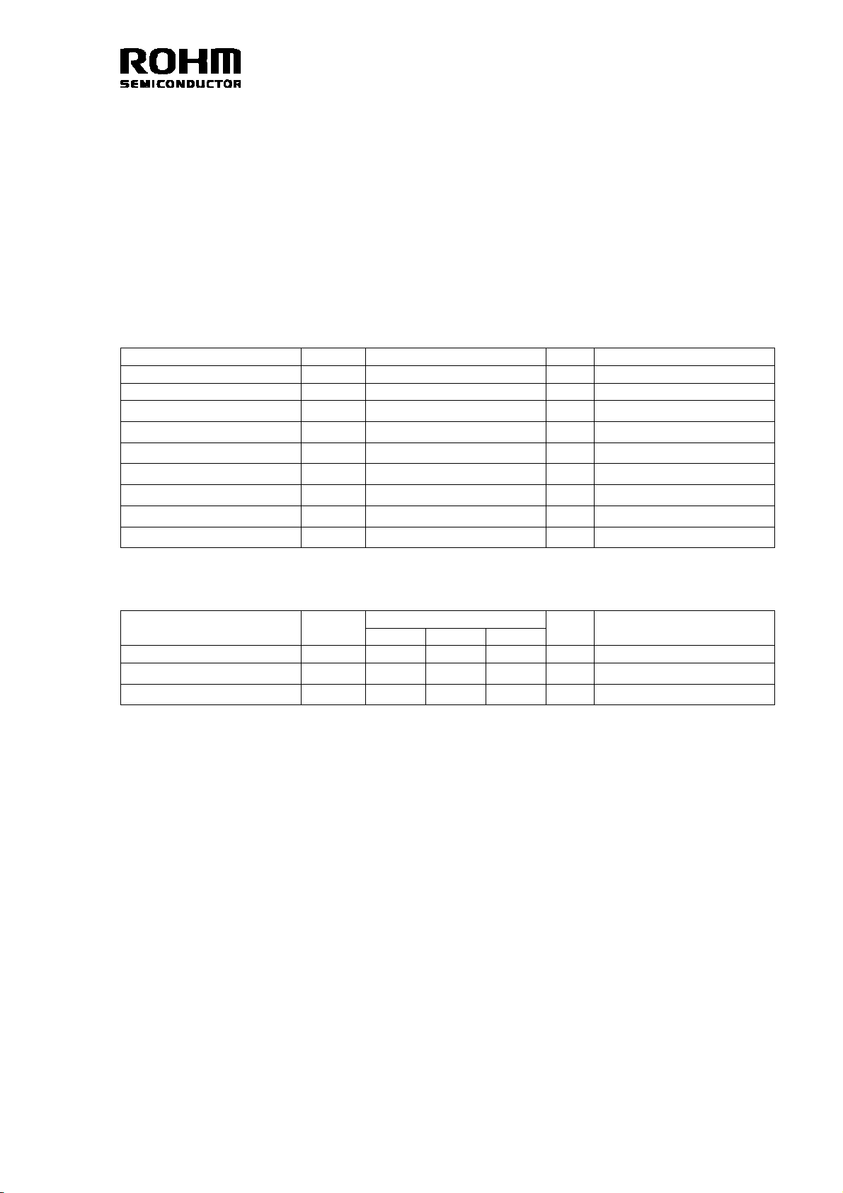
○Absolute Maximum Ratings(Ta=25
Parameter Symbol Rating Unit Remarks
Analog supply voltage AVD D
Digital supply voltage DVDD
Power supply voltage PVDD
Analog input voltage V
Digital input voltage V
Input current IIN
Allowable dissipation Pd 310(*1) mW
Operating temperature range T
Storage temperature range T
(*1) When Ta is above 25oC, reduce 3.1mW per 1oC.
○Recommended operating conditions(Ta =2 5
Parameter Symbol
Analog operation voltage AVDD 2.7 2.8 3.1 V (*2)
Digital operation voltage DVDD 1.65 1.8 3.1
Power operation voltage PVDD 2.7 2.8 3.1
(*2) AVDD and PVDD are internally connected in the IC and use the same potential.
This chip is not designed to protect itself against radioactive rays.
C)
AIN
DIN
OPR
STG
-0.3~4.5
-0.3~4.5
-0.3~4.5
AVSS-0.3~AVDD+0.3
DVSS-0.3~DVDD+0.3
-10~+10
o
-30~+85
-55~+125
C)
Rating
Min. Typ. Max.
V
V
V
V
V
mA
o
C
o
C
Unit Remarks
V
V
REV. B
2/4
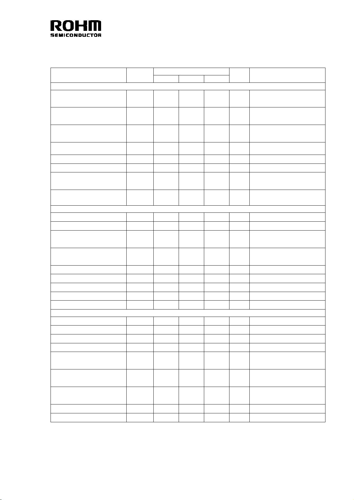
○Electrical Characteristics
(Unless otherwise noted, Ta = 25oC AVSS=DVSS=PVSS=0.0V ATT is set at 0)
Parameter Symbol
Min. Typ. Max.
Digital DC characteristics
Digital high level input
voltage 1
Digital high level input
voltage 2
Digital low level input voltage
1
Digital low level input voltage
2
V
IH1
V
IH2
V
V
Digital high level input current IIH
Digital low level input current IIL
Digital high level output
voltage
Digital low level output
voltage
VOH
V
IL1
IL2
OL
0.8
DVDD
DVDD
-0.4
- - 0.2
- - 0.4 V
- - 1
- - 1
DVDD
-0.5
- - 0.5 V
Digital AC characteristics
SCL clock frequency f
Bus free time t
(Iterative) start condition
setup time
(Iterative) start condition hold
time
SCL low time t
SCL high time t
Data setup time t
Data hold time t
Stop condition setup time t
- - 400 kHz
SCL
1.3 - - μs
BUF
t
0.6 - - μs
SU;STA
t
0.6 - - μs
HD;STA
1.3 - - μs
LOW
0.6 - - μs
HIGH
100 - - ns
SU;DAT
0 - - ns
HD;DAT
0.6 - - μs
SU;STO
Current consumption AVDD=DVDD=PVDD=2.8V input signal = no signal.
Standby current IST - - 3 μA
TX_OUT path current I
HF_OUT path current I
BT_OUT path current I
Reciever path current I
Headphone path current I
Speaker path current I
Full operation current I
Microphone bias current I
- 1.3 2.2 mA
DD1
- 1.4 2.4 mA
DD2
- 1.3 2.2 mA
DD3
- 2.5 4.2 mA
DD4
- 3.5 5.9 mA
DD5
- 1.9 3.2 mA
DD6
- 8.5 13.5 mA
DD9
- 250 430 μA
DD8
Rating
- - V
- - V
DVDD
- - V
Unit Condition
DVDD=3.0V
DVDD=1.8V
DVDD=3.0V
V
DVDD=1.8V
VIH=DVDD
μA
VIL=DVSS
μA
IOH=-1mA
IOL=1mA
After a reset
MIC1_IN→MIX6→TX_OUT
RX_IN→MIX2→HF_OUT
RX_IN→MIX2→BT_OUT
RX_IN→MIX2→RCVP_OUT、
RCVN_OUT
DACL_IN→MIX2→HPL_OUT
DACR_IN→MIX3→HPR_OUT
DACL_IN→MIX4→SPL_OUT
DACR_IN→MIX5→SPR_OUT
All paths are ON
BIAS_ON=!
REV. B

3/4
○External measure and View ○Pin layout diagram
BU78
43AGU
LOT No
VBGA063T050 (Unit: mm)
○Block diagram
Pin
NO.
Pin name
Pin
NO.
Pin name
Pin
NO.
Pin name
A1 N.C. F4 KB0 C8 RCVP_OUT
C3 MIC1_IN H4 DVDD C7 CPOP
C2 MIC2_IN G5 DVSS B8 N.C.
D2 MIC3_IN F5 KB1 B7 N.C.
C1 AUX1_IN H5 KB2 A8 N.C.
D3 DACR_IN E5 KB3 A7 N.C.
D1 AUX2_IN H6 KB4 C6 SPL_OUT
E2 DACL_IN G6 KB5 B6 SPR_OUT
E3 RX_IN H7 N.C. B5 HF_OUT
E1 SDA G7 N.C. A6 BT_OUT
E4 SDL H8 N.C. C5 TX_OUT
F1 KBR0 G8 N.C. A5 COMOUT
F2 KBR1 F6 IRQ B4 COMIN
G1 N.C. F7 RSTB C4 AVDD
G2 N.C. F8 HPR_OUT A4 AVSS
H1 N.C. E6 HPL_OUT D4 CBIAS
H2 N.C. E8 CHPL A3 MIC1_OUT
F3 KBR2 D7 PVSS B3 MICB
G3 KBR3 D6 PVDD A2 N.C.
G4 KBR4 D8 RCVN_OUT B3 N.C.
H3 KBR5 D5 CSTEP
MIC1_IN
MIC2_IN
MIC3_IN
AUX1_IN
DACR_IN
AUX2_IN
DACL_IN
RX_IN
KBR0
KBR1
N.C.
63
64
B2
1
A1
N.C.
3
-
C3
+
MIC AMP
4
C2
5
D2
6
AUX1_V
C1
-11~ +3dB/1dB
7
DACR_V
D3
-11~ +3dB/1dB
8
AUX2_V
D1
-11~ +3dB/1dB
9
DACL_V
E2
-11~ +3dB/1dB
10
RX_V
E3
-11~ +3dB/1dB
11
E1
SDA
12
SCL
13
14
15
N.C.
16
N.C.
I2C BUS I/FKEYSCAN
E4
DVDD
30k
F1
DVDD
30k
F2
G1
G2
6
H1
17
18
N.C.
61
62
B3
A2
MIC_BIAS AVDD / AVSS VREF
SW
SW
SW
DVDD
DVDD
30k
F3
H2
19
20
N.C.
KBR2
A3
MIC_V
-20~ +3 0dB/2dB
30k
G3
KBR3
59
60
D4
+
MIX1
+
MIX2
+
MIX3
+
MIX5
+
MIX4
DVDD
DVDD
30k
G4
21
22
KBR4
57
58
A4
C4
30k
F4
H3
23
24
KB0
KBR5
B4
DVDD / DVSS
H4
DVDD
56
A5
G5
25
55
MIX6
+
AVDD/PVDD is connected at internal ,
and they are connected analog portion .
26
DVSS
53
54
A6
C5
TX_V
BT_V
-26~ +4dB/2dB
-26~ +4dB/2dB
F5
H5
27
28
KB1
KB2
B5
600OSingle
HF_V
-26~ +4dB/2dB
E5
KB3
52
RCV_V
-26~ +4dB/2dB
HPL_V
-26~ +4dB/2dB
HPR_V
-26~ +4dB/2dB
29
51
B6
SPR_V
-26~ +12dB/2dB
H6
30
KB4
C6
SPL_V
G6
50
-26~ + 12dB/2dB
6
6
31
KB5
49
A8
A7
MUTE
ANTI-POP
32OBTL
AVDD / AVSS
16OSingle
16OSingle
KEYSCAN
BU7843AGU
H7
G7
32
N.C.
N.C.
B7
48
N.C.
B8
47
CPOP
C7
46
RCVP_OUT
C8
45
CSTEP
D5
44
RCVN_OUT
D8
43
PVDD
D6
42
PVSS
D7
41
CHPL
E8
40
HPL_OUT
E6
39
HPR_OUT
F8
38
CHPR
E7
37
RSTB
F7
36
IRQ
F6
35
N.C.
G8
34
N.C.
H8
33
N.C.
N.C.
N.C.
SPL_OUT
SPR_OUT
HF_OUT
BT_OUT
TX_OUT
COMOUT
COMIN
AVDD
AVSS
CBIAS
MIC1_OUT
MICB
N.C.
REV. B

4/4
Cautions on use
○
(1) Absolute Maximum Ratings
An excess in the absolute maximum ratings, such as supply voltage, temperature range of operating conditions, etc.,
can break down devices, thus making impossible to identify breaking mode such as a short circuit or an open circuit. If
any special mode exceeding the absolute maximum ratings is assumed, consideration should be given to take physical
safety measures including the use of fuses, etc.
(2) Operating conditions
These conditions represent a range within which characteristics can be provided approximately as expected. The
electrical characteristics are guaranteed under the conditions of each parameter.
(3) Reverse connection of power supply connector
The reverse connection of power supply connector can break down ICs. Take protective measures against the
breakdown due to the reverse connection, such as mounting an external diode between the power supply and the
IC’s power supply terminal.
(4) Power supply line
Design PCB pattern to provide low impedance for the wiring between the power supply and the GND lines.In this
regard, for the digital block power supply and the analog block power supply, even though these power supplies has the
same level of potential, separate the power supply pattern for the digital block from that for the analog block, thus
suppressing the diffraction of digital noises to the analog block power supply resulting from impedance common to the
wiring patterns. For the GND line, give consideration to design the patterns in a similar manner.
Furthermore, for all power supply terminals to ICs, mount a capacitor between the power supply and the GND terminal.
At the same time, in order to use an electrolytic capacitor, thoroughly check to be sure the characteristics of the
capacitor to be used present no problem including the occurrence of capacity dropout at a low temperature, thus
determining the constant.
(5) GND voltage
Make setting of the potential of the GND terminal so that it will be maintained at the minimum in any operating state.
Furthermore, check to be sure no terminals are at a potential lower than the GND voltage including an actual electric
transient.
(6) Short circuit between terminals and erroneous mounting
In order to mount ICs on a set PCB, pay thorough attention to the direction and offset of the ICs. Erroneous mounting
can break down the ICs. Furthermore, if a short circuit occurs due to foreign matters entering between terminals or
between the terminal and the power supply or the GND terminal, the ICs can break down.
(7) Operation in strong electromagnetic field
Be noted that using ICs in the strong electromagnetic field can malfunction them.
(8) Inspection with set PCB
On the inspection with the set PCB, if a capacitor is connected to a low-impedance IC terminal, the IC can suffer
stress. Therefore, be sure to discharge from the set PCB by each process. Furthermore, in order to mount or
dismount the set PCB to/from the jig for the inspection process, be sure to turn OFF the power supply and then mount
the set PCB to the jig. After the completion of the inspection, be sure to turn OFF the power supply and then dismount
it from the jig. In addition, for protection against static electricity, establish a ground for the assembly process and pay
thorough attention to the transportation and the storage of the set PCB.
(9) Input terminals
In terms of the construction of IC, parasitic elements are inevitably formed in relation to potential. The operation of the
parasitic element can cause interference with circuit operation, thus resulting in a malfunction and then breakdown of
the input terminal. Therefore, pay thorough attention not to handle the input terminals, such as to apply to the input
terminals a voltage lower than the GND respectively, so that any parasitic element will operate. Furthermore, do not
apply a voltage to the input terminals when no power supply voltage is applied to the IC. In addition, even if the power
supply voltage is applied, apply to the input terminals a voltage lower than the power supply voltage or within the
guaranteed value of electrical characteristics.
(10) Ground wiring pattern
If small-signal GND and large-current GND are provided, It will be recommended to separate the large-current GND
pattern from the small-signal GND pattern and establish a single ground at the reference point of the set PCB so that
resistance to the wiring pattern and voltage fluctuations due to a large current will cause no fluctuations in voltages of
the small-signal GND. Pay attention not to cause fluctuations in the GND wiring pattern of external parts as well.
(11) External capacitor
In order to use a ceramic capacitor as the external capacitor, determine the constant with consideration given to a
degradation in the nominal capacitance due to DC bias and changes in the capacitance due to temperature, etc.
(12) Others
In case of use this LSI, please peruse some other detail documents, we called ,Technical note, Functinal description,
Application note.
REV. B

Notes
No copying or reproduction of this document, in part or in whole, is permitted without the
consent of ROHM Co.,Ltd.
The content specied herein is subject to change for improvement without notice.
The content specied herein is for the purpose of introducing ROHM's products (hereinafter
"Products"). If you wish to use any such Product, please be sure to refer to the specications,
which can be obtained from ROHM upon request.
Examples of application circuits, circuit constants and any other information contained herein
illustrate the standard usage and operations of the Products. The peripheral conditions must
be taken into account when designing circuits for mass production.
Great care was taken in ensuring the accuracy of the information specied in this document.
However, should you incur any damage arising from any inaccuracy or misprint of such
information, ROHM shall bear no responsibility for such damage.
The technical information specied herein is intended only to show the typical functions of and
examples of application circuits for the Products. ROHM does not grant you, explicitly or
implicitly, any license to use or exercise intellectual property or other rights held by ROHM and
other parties. ROHM shall bear no responsibility whatsoever for any dispute arising from the
use of such technical information.
The Products specied in this document are intended to be used with general-use electronic
equipment or devices (such as audio visual equipment, of ce-automation equipment, communication devices, electronic appliances and amusement devices).
The Products specied in this document are not designed to be radiation tolerant.
While ROHM always makes effor ts to enhance the quality and reliability of its Products, a
Product may fail or malfunction for a variety of reasons.
Please be sure to implement in your equipment using the Products safety measures to guard
against the possibility of physical injur y, re or any other damage caused in the event of the
failure of any Product, such as derating, redundancy, re control and fail-safe designs. ROHM
shall bear no responsibility whatsoever for your use of any Product outside of the prescribed
scope or not in accordance with the instruction manual.
The Products are not designed or manufactured to be used with any equipment, device or
system which requires an extremely high level of reliability the failure or malfunction of which
may result in a direct threat to human life or create a risk of human injury (such as a medical
instrument, transportation equipment, aerospace machinery, nuclear-reactor controller, fuelcontroller or other safety device). ROHM shall bear no responsibility in any way for use of any
of the Products for the above special purposes. If a Product is intended to be used for any
such special purpose, please contact a ROHM sales representative before purchasing.
If you intend to export or ship overseas any Product or technology specied herein that may
be controlled under the Foreign Exchange and the Foreign Trade Law, you will be required to
obtain a license or permit under the Law.
Notice
Thank you for your accessing to ROHM product informations.
More detail product informations and catalogs are available, please contact us.
ROHM Customer Support System
www.rohm.com
© 2011 ROHM Co., Ltd. All rights reserved.
http://www.rohm.com/contact/
R1120
A
 Loading...