

Page 1

A
Operational Amplifiers / Comparators
High Speed with Low Voltage
CMOS Operational Amplifiers
Input-Output Full Swing
BU7291G,BU7291SG,BU7255HFV,BU7255SHFV
Ground sense
BU7495HFV,BU7495SHFV,BU7481G,BU7481SG
BU7485G,BU7485SG,BU5281G,BU5281SG
●Description
Low Voltage with High Speed CMOS Op-Amp integrates one independent output full swing Op-Amps and phase
compensation capacitors on a single chip. Especially, this series is operable with low voltage, low supply current, high speed
and low input bias current.
・Input-Output Full Swing
BU7291 family, BU7255 family
・Ground sense
BU7495 family, BU7481 family,
BU7485 family, BU5281 family
●Features
1) Low operating supply voltage
+2.4 [V] ~ +5.5 [V] (single supply): BU7291 family
BU7255 family
+1.8 [V] ~ +5.5 [V] (single supply): BU7495 family
BU7481 family
BU5281 family
+3.0 [V] ~ +5.5 [V] (single supply): BU7485 family
2) High large signal voltage gain
3) Internal ESD protection
Human body model (HBM) ±4000 [V] (Typ.)
4) Low input bias current 1[pA] (Typ.)
●Pin Assignments
BU7291G BU7291SG
BU7485G BU7485SG
BU7481G BU7481SG
BU5281G BU5281SG
High Speed Input-Output Full Swing Single
+IN
1
VSS
-IN
2
3
SSOP5
Ground Sense Single
5) High slew rate
3.0 [V/μs]: BU7291 family
3.4 [V/μs]: BU7255 family
5.0 [V/μs]: BU7495 family
3.2 [V/μs]: BU7481 family
2.0 [V/μs]: BU5281 family
10.0 [V/μs]: BU7485 family
VDD
5
+
-
4
OUT
HVSOF5
BU7255HFV
BU7495HFV BU7495SHFV
BU7255SHFV
Single
Single
Single
Single
BU7291G
(BU7291SG:Operation guaranteed up to +105℃)
BU7255HFV
(BU7255SHFV:Operation guaranteed up to +105℃)
BU7481G
(BU7481SG:Operation guaranteed up to +105℃)
BU7485G
(BU7485SG:Operation guaranteed up to +105℃)
BU5281G
(BU5281SG:Operation guaranteed up to +105℃)
BU7495HFV
(BU7495SHFV:Operation guaranteed up to +105℃)
No.10049EAT20
www.rohm.com
© 2010 ROHM Co., Ltd. All rights reserved.
1/26
2010.12 - Rev.
Page 2
A
BU7291G,BU7291SG,BU7255HFV,BU7255SHFV,
BU7495HFV,BU7495SHFV,BU7481G,BU7481SG,BU7485G,BU7485SG,BU5281G,BU5281SG
Technical Note
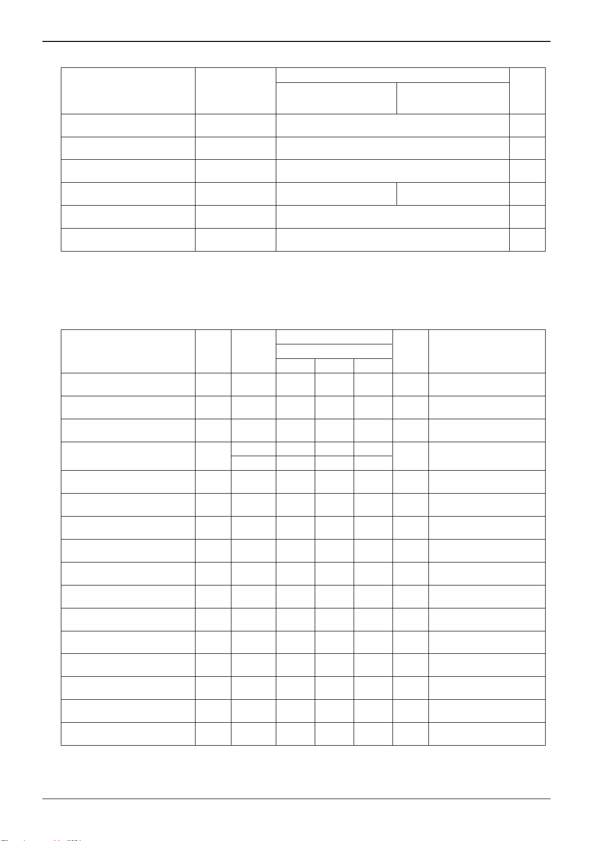
●Absolute Maximum Ratings(Ta=25[℃])
Ratings
Parameter Symbol
BU7291G, BU7255HFV
BU7495HFV, BU7481G
BU7485G, BU5281G
BU7291SG, BU7255SHFV
BU7495SHFV, BU7481SG
BU7485SG, BU5281SG
Supply Voltage VDD - VSS +7 V
Unit
Differential Input Voltage
Input Common-mode
Voltage Range
(*1)
Vid VDD - VSS V
Vicm (VSS - 0.3) ~ (VDD + 0.3) V
Operating Temperature Topr - 40 ~ +85 - 40 ~ +105 ℃
Storage Temperature Tstg - 55 ~ +125 ℃
Maximum
Junction Temperature
Note: Absolute maximum rating item indicates the condition which must not be exceeded.
Application of voltage in excess of absolute maximum rating or use out absolute maximum rated
temperature environment may cause deterioration of characteristics.
(*1) The voltage difference between inverting input and non-inverting input is the differential input voltage.
Then input terminal voltage is set to more than VSS.
Tjmax +125 ℃
●Electrical characteristics: Input-Output Full Swing
○BU7291 family(Unless otherwise specified VDD=+3[V], VSS=0[V], Ta=25[℃])
Limits
Parameter Symbol
Temperature
Range
BU7291G, BU7291SG
Unit Condition
Min. Typ. Max.
Input Offset Voltage
Input Offset Current
Input Bias Current
(*2)
Vio 25℃ - 1 9 mV -
(*2)
Iio 25℃ - 1 - pA -
(*2)
Ib 25℃ - 1 - pA -
Supply Current
(*3)
IDD
25℃ - 470 800
Full range - - 1100
RL=∞ All Op-Amps
μA
AV=0[dB],VIN=1.5[V]
High Level Output Voltage VOH 25℃ VDD-0.1 - - V RL=10[kΩ]
Low Level Output Voltage VOL 25℃ - - VSS+0.1 V RL=10[kΩ]
Large Signal Voltage Gain AV 25℃ 70 105 - dB RL=10[kΩ]
Input Common-mode
Voltage Range
Vicm 25℃ 0 - 3 V VSS ~ VDD
Common-mode Rejection Ratio CMRR 25℃ 40 60 - dB -
Power Supply Rejection Ratio PSRR 25℃ 45 80 - dB -
Output Source Current
Output Sink Current
(*4)
IOH 25℃ 5 8 - mA VDD-0.4[V]
(*4)
IOL 25℃ 9 16 - mA VSS+0.4[V]
Slew Rate SR 25℃ - 3.0 - V/μs CL=25[pF]
Gain Band width FT 25℃ - 2.8 - MHz CL=25[pF], AV=40[dB]
Phase Margin θ 25℃ - 50 - ° CL=25[pF], AV=40[dB]
Total Harmonic Distortion THD 25℃ - 0.03 - % VOUT=0.8[Vp-p],f=1[kHz]
(*2) Absolute value
(*3) Full range BU7291: Ta=-40[℃]~+85[℃] BU7291S: Ta=-40[℃]~+105[℃]
(*4) Under the high temperature environment, consider the power dissipation of IC when selecting the output current.
When the terminal short circuits are continuously output, the output current is reduced to climb to the temperature inside IC.
www.rohm.com
© 2010 ROHM Co., Ltd. All rights reserved.
2/26
2010.12 - Rev.
Page 3

A
BU7291G,BU7291SG,BU7255HFV,BU7255SHFV,
BU7495HFV,BU7495SHFV,BU7481G,BU7481SG,BU7485G,BU7485SG,BU5281G,BU5281SG
○BU7255(Unless otherwise specified VDD=+3[V], VSS=0[V], Ta=25[℃])
Limits
Parameter Symbol
Temperature
Range
BU7255HFV, BU7255SHFV
Unit Condition
Min. Typ. Max.
Input Offset Voltage
(*5)
Vio 25℃ - 1 9 mV -
Technical Note
Input Offset Current
Input Bias Current
Supply Current
(*5)
Iio 25℃ - 1 - pA -
(*5)
Ib 25℃ - 1 - pA -
(*6)
IDD
25℃ - 540 900
Full range - - 1200
RL=∞ All Op-Amps
μA
AV=0[dB],VIN=1.5[V]
High Level Output Voltage VOH 25℃ VDD-0.1 - - V RL=10[kΩ]
Low Level Output Voltage VOL 25℃ - - VSS+0.1 V RL=10[kΩ]
Large Signal Voltage Gain AV 25℃ 60 105 - dB RL=10[kΩ]
Input Common-mode
Voltage Range
Vicm 25℃ 0 - 3 V VSS ~ VDD
Common-mode Rejection Ratio CMRR 25℃ 40 60 - dB -
Power Supply Rejection Ratio PSRR 25℃ 45 80 - dB -
Output Source Current
Output Sink Current
(*7)
IOH 25℃ 2 4 - mA VDD - 0.4[V]
(*7)
IOL 25℃ 4 8 - mA VSS + 0.4[V]
Slew Rate SR 25℃ - 3.4 - V/μs CL=25[pF]
Gain Band width FT 25℃ - 4 - MHz CL=25[pF], AV=40[dB]
Phase Margin θ 25℃ - 40 - ° CL=25[pF], AV=40[dB]
(*5) Absolute value
(*6) Full range BU7255: Ta=-40[℃]~+85[℃] BU7255S: Ta=-40[℃]~+105[℃]
(*7) Under the high temperature environment, consider the power dissipation of IC when selecting the output current.
When the terminal short circuits are continuously output, the output current is reduced to climb to the temperature inside IC.
www.rohm.com
© 2010 ROHM Co., Ltd. All rights reserved.
3/26
2010.12 - Rev.
Page 4

A
BU7291G,BU7291SG,BU7255HFV,BU7255SHFV,
BU7495HFV,BU7495SHFV,BU7481G,BU7481SG,BU7485G,BU7485SG,BU5281G,BU5281SG
○BU7495 family(Unless otherwise specified VDD=+3[V], VSS=0[V], Ta=25[℃])
Limits
Parameter Symbol
Temperature
Range
BU7495HFV, BU7495SHFV
Unit Condition
Min. Typ. Max.
Input Offset Voltage
(*8)
Vio 25℃ - 1 6 mV -
Technical Note
Input Offset Current
Input Bias Current
Supply Current
(*8)
Iio 25℃ - 1 - pA -
(*8)
Ib 25℃ - 1 - pA -
(*9)
IDD
25℃ - 650 1150
Full range - - 1350
RL=∞ All Op-Amps
μA
AV=0[dB],VIN=0.9[V]
High Level Output Voltage VOH 25℃ VDD-0.1 - - V RL=10[kΩ]
Low Level Output Voltage VOL 25℃ - - VSS+0.1 V RL=10[kΩ]
Large Signal Voltage Gain AV 25℃ 60 100 - dB RL=10[kΩ]
Input Common-mode
Voltage Range
Vicm 25℃ 0 - 1.8 V VSS ~ VDD-1.2[V]
Common-mode Rejection Ratio CMRR 25℃ 45 60 - dB -
Power Supply Rejection Ratio PSRR 25℃ 60 80 - dB -
Output Source Current
Output Sink Current
(*10)
IOH 25℃ 4 7 - mA VDD - 0.4[V]
(*10)
IOL 25℃ 9 14 - mA VSS + 0.4[V]
Slew Rate SR 25℃ - 5.0 - V/μs CL=25[pF]
Gain Band width FT 25℃ - 4 - MHz CL=25[pF], AV=40[dB]
Phase Margin θ 25℃ - 50 - ° CL=25[pF], AV=40[dB]
Total Harmonic Distortion THD 25℃ - 0.03 - % VOUT=0.8[Vp-p], f=1[kHz]
(*8) Absolute value
(*9) Full range BU7495: Ta=-40[℃]~+85[℃] BU7495S: Ta=-40[℃]~+105[℃]
(*10) Under the high temperature environment, consider the power dissipation of IC when selecting the output current.
When the terminal short circuits are continuously output, the output current is reduced to climb to the temperature inside IC
www.rohm.com
© 2010 ROHM Co., Ltd. All rights reserved.
4/26
2010.12 - Rev.
Page 5

A
BU7291G,BU7291SG,BU7255HFV,BU7255SHFV,
BU7495HFV,BU7495SHFV,BU7481G,BU7481SG,BU7485G,BU7485SG,BU5281G,BU5281SG
○BU7481 family(Unless otherwise specified VDD=+3[V], VSS=0[V], Ta=25[℃])
Limits
Parameter Symbol
Temperature
Range
BU7481G, BU7481SG
Unit Condition
Min. Typ. Max.
Input Offset Voltage
(*11)
Vio 25℃ - 1 8 mV -
Technical Note
Input Offset Current
Input Bias Current
Supply Current
(*11)
Iio 25℃ - 1 - pA -
(*11)
Ib 25℃ - 1 - pA -
(*12)
IDD
25℃ - 420 750
Full range - - 900
RL=∞ All Op-Amps
μA
AV=0[dB],VIN=0.9[V]
High Level Output Voltage VOH 25℃ VDD-0.1 - - V RL=10[kΩ]
Low Level Output Voltage VOL 25℃ - - VSS+0.1 V RL=10[kΩ]
Large Signal Voltage Gain AV 25℃ 70 105 - dB RL=10[kΩ]
Input Common-mode
Voltage Range
Vicm 25℃ 0 - 1.8 V VSS ~ VDD-1.2[V]
Common-mode Rejection Ratio CMRR 25℃ 45 60 - dB -
Power Supply Rejection Ratio PSRR 25℃ 60 80 - dB -
Output Source Current
Output Sink Current
(*13)
IOH 25℃ 5 8 - mA VDD - 0.4[V]
(*13)
IOL 25℃ 9 16 - mA VSS + 0.4[V]
Slew Rate SR 25℃ - 3.2 - V/μs CL=25[pF]
Gain Band width FT 25℃ - 2.8 - MHz CL=25[pF], AV=40[dB]
Phase Margin θ 25℃ - 50 - ° CL=25[pF], AV=40[dB]
Total Harmonic Distortion THD 25℃ - 0.03 - % VOUT=0.8[Vp-p], f=1[kHz]
(*11) Absolute value
(*12) Full range BU7481: Ta=-40[℃]~+85[℃] BU7481S: Ta=-40[℃]~+105[℃]
(*13) Under the high temperature environment, consider the power dissipation of IC when selecting the output current.
When the terminal short circuits are continuously output, the output current is reduced to climb to the temperature inside IC.
www.rohm.com
© 2010 ROHM Co., Ltd. All rights reserved.
5/26
2010.12 - Rev.
Page 6

A
BU7291G,BU7291SG,BU7255HFV,BU7255SHFV,
BU7495HFV,BU7495SHFV,BU7481G,BU7481SG,BU7485G,BU7485SG,BU5281G,BU5281SG
○BU7485 family(Unless otherwise specified VDD=+3[V], VSS=0[V], Ta=25[℃])
Limits
Parameter Symbol
Temperature
Range
BU7485G, BU7485SG
Unit Condition
Min. Typ. Max.
Input Offset Voltage
(*14)
Vio 25℃ - 1 9.5 mV -
Technical Note
Input Offset Current
Input Bias Current
Supply Current
(*14)
Iio 25℃ - 1 - pA -
(*14)
Ib 25℃ - 1 - pA -
(*15)
IDD
25℃ - 1500 2000
Full range - - 2400
RL=∞ All Op-Amps
μA
AV=0[dB],VIN=0.8[V]
High Level Output Voltage VOH 25℃ VDD-0.1 - - V RL=10[kΩ]
Low Level Output Voltage VOL 25℃ - - VSS+0.1 V RL=10[kΩ]
Large Signal Voltage Gain AV 25℃ 70 105 - dB RL=10[kΩ]
Input Common-mode
Voltage Range
Vicm 25℃ 0 - 1.6 V VSS ~ VDD-1.4[V]
Common-mode Rejection Ratio CMRR 25℃ 45 60 - dB -
Power Supply Rejection Ratio PSRR 25℃ 60 80 - dB -
Output Source Current
Output Sink Current
(*16)
IOH 25℃ 4 8 - mA VDD-0.4[V]
(*16)
IOL 25℃ 7 12 - mA VSS + 0.4[V]
Slew Rate SR 25℃ - 10 - V/μs CL=25[pF]
Gain Band width FT 25℃ - 10 - MHz CL=25[pF], AV=40[dB]
Phase Margin θ 25℃ - 50 - ° CL=25[pF], AV=40[dB]
Total Harmonic Distortion THD 25℃ - 0.03 - % VOUT=0.7[Vp-p], f=1[kHz]
(*14) Absolute value
(*15) Full range BU7485: Ta=-40[℃]~+85[℃] BU7485S: Ta=-40[℃]~+105[℃]
(*16) Under the high temperature environment, consider the power dissipation of IC when selecting the output current.
When the terminal short circuits are continuously output, the output current is reduced to climb to the temperature inside IC.
www.rohm.com
© 2010 ROHM Co., Ltd. All rights reserved.
6/26
2010.12 - Rev.
Page 7

A
BU7291G,BU7291SG,BU7255HFV,BU7255SHFV,
BU7495HFV,BU7495SHFV,BU7481G,BU7481SG,BU7485G,BU7485SG,BU5281G,BU5281SG
○BU5281 family(Unless otherwise specified VDD=+3[V], VSS=0[V], Ta=25[℃])
Limits
Parameter Symbol
Temperature
Range
BU5281G, BU5281SG
Unit Condition
Min. Typ. Max.
Input Offset Voltage
(*17)
Vio 25℃ - 0.1 2.5 mV -
Technical Note
Input Offset Voltage drift
Input Offset Current
Input Bias Current
Supply Current
(*18)
(*17)
ΔVio/ΔT - - 0.8 - μV/℃ -
(*17)
Iio 25℃ - 1 - pA -
(*17)
Ib 25℃ - 1 - pA -
IDD
25℃ - 750 1000
Full range - - 1200
RL=∞ All Op-Amps
μA
AV=0[dB],VIN=0.9[V]
High Level Output Voltage VOH 25℃ VDD-0.1 - - V RL=10[kΩ]
Low Level Output Voltage VOL 25℃ - - VSS+0.1 V RL=10[kΩ]
Large Signal Voltage Gain AV 25℃ 70 110 - dB RL=10[kΩ]
Input Common-mode
Voltage Range
Vicm 25℃ 0 - 1.8 V VSS ~ VDD - 1.2[V]
Common-mode Rejection Ratio CMRR 25℃ 45 60 - dB -
Power Supply Rejection Ratio PSRR 25℃ 60 80 - dB -
Output Source Current
Output Sink Current
(*19)
IOH 25℃ 5 8 - mA VDD-0.4[V]
(*19)
IOL 25℃ 10 16 - mA VSS+0.4[V]
Slew Rate SR 25℃ - 2.0 - V/μs CL=25[pF]
Gain Band width FT 25℃ - 3 - MHz CL=25[pF], AV=40[dB]
Phase Margin θ 25℃ - 40 - ° CL=25[pF], AV=40[dB]
1/2
- 18 - nV/(Hz)
AV=40[dB], f=1[kHz]
Input Referred Noise Voltage Vin 25℃
- 3.2 - μVrms AV=40[dB], DINAUDIO
Total Harmonic Distortion THD 25℃ - 0.003 - % VOUT=0.4[Vp-p], f=1[kHz]
(*17) Absolute value
(*18) Full range BU5281: Ta=-40[℃]~+85[℃] BU5281S: Ta=-40[℃]~+105[℃]
(*19) Under the high temperature environment, consider the power dissipation of IC when selecting the output current.
When the terminal short circuits are continuously output, the output current is reduced to climb to the temperature inside IC.
www.rohm.com
© 2010 ROHM Co., Ltd. All rights reserved.
7/26
2010.12 - Rev.
Page 8

A
BU7291G,BU7291SG,BU7255HFV,BU7255SHFV,
y
y
y
y
–
–
–
–
–
–
–
BU7495HFV,BU7495SHFV,BU7481G,BU7481SG,BU7485G,BU7485SG,BU5281G,BU5281SG
●Reference Data (BU7291 family)
800
600
400
200
POWER DISSIP ATION [mW] .
0
0 5 0 100 15 0
Fig.1 Fig.2 Fig.3
100 0
80 0
60 0
40 0
S UPPLY CUR RENT [μA]
20 0
0
-60-30 0 306090120
Fig.4 Fig.5 Fig.6
Ambient Temperature
20
15
10
-40℃ 25℃ 85℃
5
OUTPUT VOLTAGE LOW [mV]
0
23456
Fig.7 Fig.8 Fig.9
Supply Voltage (RL=10[kΩ])
20
15
10
5
OUTPUT SOURCE CURRENT [mA]
0
-60 -30 0 30 60 90 120
Fig.10 Fig.11 Fig.12
Output Source Current – Ambient Temperature
(VOUT=VDD-0.4[V])
BU7291G
AMBIEN T TEMPER ATURE [℃]
Derating curve
2.4V
AMBIE NT TE MPERATU RE [℃]
Supply Current
SUPPLY VOLTAG E [ V]
Output Voltage Low
5.5V
3.0V
2.4V
AMBIENT TEMPERATURE [℃]
(*)The above data is ability value of sample, it is not guaranteed.BU7291G: -40[℃] ~ +85[℃] BU7291SG: -40[℃] ~ +105[℃]
85
5.5V
3.0V
BU7291 famil
BU7291 family
BU7291 famil
105℃
BU7291 family
800
600
BU7291SG
400
200
POWER DISSIP ATION [m W] .
0
0 5 0 100 15 0
AMBIEN T TEMPER ATURE [℃]
BU7291 family
105
Derating curve
6
5
4
3
2
1
OUTPUT VOLTAGE HIGH [V]
0
123456
105℃
85℃
-40℃
SUPPL Y VOLTAGE [V]
BU7291 family
25℃
Output Voltage High
Supply Voltage (RL=10[kΩ])
20
15
10
5
O UTPUT VOLTAGE LOW [m V]
0
-60-30 0 30 60 90120
3.0V
2.4V
AMBIENT TEMPERATURE [℃]
BU7291 family
5.5V
Output Voltage Low
Ambient Temperature (RL=10[kΩ])
105℃
BU7291 family
85℃
80
-40℃
60
25℃
40
20
OUT PUT SINK CURREN T [mA]
0
0.0 0.5 1.0 1.5 2.0 2.5 3.0
O UTPUT VOLTAGE [V]
Output Sink Current – Output Voltage
(VDD=3[V])
1000
800
600
400
SUPPLY CURRENT [μA]
200
0
23 456
Supply Current
6
5
4
3
2
1
OUT PUT VOLTAG E HIGH [V ]
0
-60 -30 0 30 60 90 120
AMBIEN T TEMPERATU RE [℃]
Output Voltage High
Ambient Temperature (RL=10[kΩ])
50
40
30
20
10
OUTPUT SOURCE CURRENT [mA]
0
-40℃
0 0.5 1 1. 5 2 2.5 3
Output Source Current
Output Voltage (VDD=3[V])
50
40
30
20
10
OUTPUT SINK CURRENT [mA]
0
-60-30 0 306090120
AMBIEN T TEMPER ATURE [℃]
Output Sink Current – Ambient Temperature
(VOUT=VSS+0.4[V])
Technical Note
105℃
85℃
-40℃ 25℃
SUPPLY VOLTAG E [V ]
OUTPUT V OLTAGE [V]
2.4V
Supply Voltage
5.5V
3.0V
2.4V
25℃
85℃ 105℃
5.5V
3.0V
BU7291 family
BU7291 famil
BU7291 family
BU7291 famil
www.rohm.com
© 2010 ROHM Co., Ltd. All rights reserved.
8/26
2010.12 - Rev.
Page 9

A
BU7291G,BU7291SG,BU7255HFV,BU7255SHFV,
y
y
y
y
y
y
y
y
BU7495HFV,BU7495SHFV,BU7481G,BU7481SG,BU7485G,BU7485SG,BU5281G,BU5281SG
Technical Note
●Reference Data (BU7291 family)
10 .0
7.5
5.0
2.5
0.0
-2 .5
-5 .0
-7 .5
INPU T OFFSET VOLTAGE [mV]
-10.0
23456
Fig.13 Fig.14 Fig.15
Input Offset Voltage – Supply Voltage
(Vicm=VDD, VOUT=1.5[V])
160
140
120
100
80
LARGE SIGN AL VOLTAG E GAI N [dB]
60
23456
Fig.16 Fig.17 Fig.18
Large Signal Voltage Gain
120
100
80
60
40
20
COMMON MODE REJECTION RATIO [dB]
0
-60-30 0 306090120
AMBIE NT TEM PERAT URE [℃]
Fig.19 Fig.20 Fig.21
Common Mode Rejection Ratio
– Ambient Temperature
5.0
4.0
3.0
2.0
SLEW RATE H-L [V/μs]
1.0
0.0
-60 - 30 0 30 60 90 120
AMBIEN T T EMPER ATU RE [℃]
Fig.22 Fig.23
Slew Rate H-L – Ambient Temperature
-40℃
105℃
S UPPLY V OLTAGE [V]
85℃
SUPPLY VOLTAGE [V]
– Supply Voltage
5.5V
2.4V
3.0V
5.5V
2.4V
BU7291 famil
25℃
85℃
BU7291 family
105℃
-40℃ 25℃
BU7291 family
BU7291 famil
3.0V
10.0
7.5
5.0
2.5
0.0
-2.5
-5.0
INPUT O FFSET VOLTAGE [ mV]
-7.5
-1 0.0
-60-30 0 306090120
2.4V 3.0V
AMBIEN T TEMPER ATURE [℃]
Input Offset Voltage – Ambient Temperature
(Vicm=VDD, VOUT=1.5[V])
160
140
120
100
80
LARGE S IGNAL VOLTAG E GAIN [dB]
60
-60-300 306090120
AMBIEN T TEMPER ATURE [℃]
Large Signal Voltage Gain
– Ambient Temperature
140
120
100
80
60
40
20
POWER SUPPLY REJECTION RATIO [dB]
0
-6 0 -30 0 3 0 60 90 12 0
AMBIENT TEMPERATURE [℃]
Power Supply Rejection Ratio
– Ambient Temperature
100
80
60
GAIN[d B]
40
20
0
1.E+00 1.E+01 1.E+02 1.E+03 1.E+04 1.E+05 1.E+06 1.E+07 1.E+08
Phase
Gain
FREQUENCY [Hz]
Voltage Gain-Frequency
(*)The above data is ability value of sample, it is not guaranteed. BU7291G: -40[℃] ~ +85[℃] BU7291SG: -40[℃] ~ +105[℃]
5.5V
2.4V
BU7291 famil
BU7291 family
5.5V
3.0V
BU7291 famil
BU7291 famil
200
150
100
50
0
15
10
5
0
-5
-1 0
INPU T OFFSET VOLTAGE [mV]
-1 5
-101234
85℃ 105℃
25℃
INPUT VOLTAGE [V]
BU7291 famil
-40℃
Input Offset Voltage – Input Voltage
(VDD=3[V])
120
100
80
60
40
20
COMMON MODE REJECTION RATIO [dB]
0
2 345 6
85℃
-40℃ 25℃
SUPPL Y VOLTAGE [V]
BU7291 famil
105℃
Common Mode Rejection Ratio
– Supply Voltage (VDD=3[V])
5
4
3
2
SL E W RAT E L- H [V/ μs]
1
0
-60 - 30 0 30 6 0 9 0 120
AMBIEN T TEMPER ATURE [℃]
2.4V
BU7291 famil
5.5V
Slew Rate L-H
– Ambient Temperature
PHASE [deg ]
3.0V
www.rohm.com
© 2010 ROHM Co., Ltd. All rights reserved.
9/26
2010.12 - Rev.
Page 10

A
BU7291G,BU7291SG,BU7255HFV,BU7255SHFV,
y
y
y
y
y
y
y
y
y
–
–
–
–
–
–
–
BU7495HFV,BU7495SHFV,BU7481G,BU7481SG,BU7485G,BU7485SG,BU5281G,BU5281SG
●Reference Data (BU7255 family)
1000
80 0
60 0
40 0
20 0
PO WER D ISSIPATIO N [mW ] .
0
0 50 100 150
Fig.24 Fig.25 Fig.26
15 00
12 00
900
600
SUPPL Y CURREN T [μA]
300
0
-6 0 - 30 0 30 60 90 12 0
Fig.27 Fig.28 Fig.29
20
15
10
-40℃ 25℃
5
OUT PU T VOLTA GE LOW [mV]
0
23456
Fig.30 Fig.31 Fig.32
Supply Voltage (RL=10[kΩ])
20
15
10
3.0V
5
OUTPUT SOURCE CURRENT [mA]
0
-6 0 -30 0 30 6 0 90 12 0
Fig.33 Fig.34 Fig.35
Output Source Current –Ambient Temperature
(*)The above data is ability value of sample, it is not guaranteed. BU7255HFV: -40[℃] ~ +85[℃] BU7255SHFV: -40[℃] ~ +105[℃]
BU7255HFV
85
AMBIEN T TEMPER ATURE [℃]
Derating curve
3.0V
AMBIEN T TEMPER ATU RE [℃]
Supply Current
Ambient Temperature
85℃ 105℃
SUPP LY V OLTAG E [V]
Output Voltage Low
5.5V
2.4V
A MBIENT T EMPERATU RE [
(VOUT=VDD-0.4[V])
5.5V
2.4V
BU7255
BU7255 famil
BU7255 family
BU7255 famil
℃
]
100 0
80 0
60 0
40 0
20 0
PO WER D ISS IPATIO N [mW] .
0
0 5 0 100 150
BU7255SHFV
AMBIEN T TEM PERAT URE [℃]
Derating curve
6
5
4
3
2
1
OUT PUT VOL TAGE H IGH [ V]
0
23456
105℃
85℃
-40℃
SUPP LY VOLTAGE [V]
Output Voltage High
Supply Voltage (RL=10[kΩ])
20
15
10
5
OUTPUT VOLTAGE LOW [mV]
0
-60 -30 0 30 60 90 120
2.4V
AMBIENT TEMPERATURE [℃]
Output Voltage Low
Ambient Temperature (RL=10[kΩ])
40
30
20
10
OUT PUT SINK CURRENT [m A]
25℃
85℃
0
0.0 0. 5 1.0 1. 5 2 .0 2.5 3 .0
OUT PUT VOL TAGE [V]
Output Sink Current – Output Voltage
(VDD=3[V])
-40℃
25℃
5.5V
105℃
BU7255 famil
105
BU7255 famil
BU7255 famil
3.0V
BU7255 famil
150 0
125 0
100 0
75 0
50 0
SUPPLY CURRENT [μA]
25 0
0
23456
SUPPLY VOLTAGE [V]
Supply Current
6
5
4
3
2
1
OUT PUT VOLTAG E HIGH [V]
0
-60-30 0 306090120
A MBIEN T TEMP ERAT URE [℃]
Output Voltage High
Ambient Temperature (RL=10[kΩ])
20
15
10
OUTP UT SOURCE CURRENT [mA]
-40℃
5
0
00.511.522.53
OUT PUT VOLTAG E [V]
Output Source Current
Output Voltage (VDD=3[V])
40
30
20
3.0V
10
OUTPUT SINK CURRENT [mA]
2.4V
0
-60 - 30 0 30 6 0 90 120
AMBIEN T TEMPER ATURE[℃]
Output Sink Current – Ambient Temperature
(VOUT=VSS+0.4[V])
Technical Note
BU7255 famil
105℃
85℃
-40℃
25℃
Supply Voltage
BU7255 famil
5.5V
3.0V
2.4V
BU7255 family
25℃
85℃ 105℃
5.5V
BU7255 famil
www.rohm.com
© 2010 ROHM Co., Ltd. All rights reserved.
10/26
2010.12 - Rev.
Page 11

A
BU7291G,BU7291SG,BU7255HFV,BU7255SHFV,
y
y
y
y
y
y
y
y
y
–
–
BU7495HFV,BU7495SHFV,BU7481G,BU7481SG,BU7485G,BU7485SG,BU5281G,BU5281SG
Technical Note
●Reference Data (BU7255 family)
10. 0
7. 5
5. 0
2. 5
0. 0
-2.5
-5.0
INPUT OF FSET VOL TAGE [mV ]
-7.5
-10. 0
234 56
Fig.36 Fig.37 Fig.38
Input Offset Voltage – Supply Voltage
14 0
12 0
10 0
80
60
40
20
LARGE SIGNAL VOLTAGE G AIN [d B]
0
2 345 6
Fig.39 Fig.40 Fig.41
12 0
10 0
80
60
40
20
C OMM ON MO DE RE JE CTI ON RATI O [d B]
0
-60-300306090120
Fig.42 Fig.43 Fig.44
Common Mode Rejection Ratio
8.0
6.0
4.0
SLEW RA TE H-L [V/μs]
2.0
0.0
-60 -30 0 30 60 90 120
Fig.45 Fig.46
Slew Rate H-L
-40℃ 25℃
SUPPLY VOLTAGE[V ]
(Vicm=VDD, VOUT=1.5V])
-40℃ 25℃
SUPPLY VOLTAGE [ V]
Large Signal Voltage Gain
– Supply Voltage
AMBIEN T TEMPER ATURE [℃]
– Ambient Temperature
2.4V
AMBIENT TEMPERATURE [℃]
Ambient Temperature
5.5V
2.4V 3.0V
5.5V
105℃
3.0V
BU7255 famil
85℃ 105℃
BU7255 family
85℃
BU7255 famil
BU7255 famil
10.0
7.5
5.0
2.5
0.0
-2.5
-5.0
INPUT OFFSET VOLTAGE [mV]
-7.5
-1 0.0
-60 -30 0 30 60 90 120
AMBIE NT TEMPER ATURE [℃]
5.5V
3.0V
Input Offset Voltage – Ambient Temperature
(Vicm=VDD, VOUT=1.5[V])
16 0
14 0
12 0
10 0
80
LARGE SIGNAL VOLTAGE G AIN [dB ]
60
-60 -30 0 30 60 9 0 120
2.4V 3.0V
AMBIEN T TEMPER ATURE [℃]
Large Signal Voltage Gain
– Ambient Temperature
140
120
100
80
60
40
20
P OWE R S UPP LY RE JEC TIO N RA TI O [d B]
0
-60 -30 0 30 60 90 120
AMBIE NT TEMPER ATURE [℃]
Power Supply Rejection Ratio
– Ambient Temperature
100
80
60
GAIN [dB]
40
20
0
1.E+00 1.E+01 1.E+02 1. E+03 1. E+04 1.E+05 1.E+06 1.E+07 1.E+08
Phase
Gain
FREQUENCY [Hz]
Voltage Gain-Frequency
(*)The above data is ability value of sample, it is not guaranteed. BU7255HFV: -40[℃] ~ +85[℃] BU7255SHFV: -40[℃] ~ +105[℃]
5.5V
2.4V
BU7255 family
BU7255 famil
BU7255 famil
BU7255 famil
20 0
15 0
10 0
50
0
15
10
5
0
-5
-10
INPU T OFFSET VOLTAG E [mV]
-15
-101234
25℃
-40℃
INPU T VOLTA GE [V ]
105℃
Input Offset Voltage – Input Voltage
(VDD=3[V])
120
100
80
60
40
20
COMMON MODE REJECTION RATIO [dB]
0
2 345 6
85℃
SUPPL Y VOLTAGE [ V]
105℃
-40℃
25℃
Common Mode Rejection Ratio
Supply Voltage (VDD=3[V])
8
6
4
2
SLEW RATE L- H [V/ μs]
0
-60-300306090120
5.5V
3.0V
2.4V
AMBI ENT TEMPER ATURE [℃]
Slew Rate L-H
– Ambient Temperature
PHASE [d eg]
BU7255 famil
85℃
BU7255 famil
BU7255 famil
www.rohm.com
© 2010 ROHM Co., Ltd. All rights reserved.
11/26
2010.12 - Rev.
Page 12

A
BU7291G,BU7291SG,BU7255HFV,BU7255SHFV,
y
y
y
y
y
y
y
y
y
y
y
–
–
BU7495HFV,BU7495SHFV,BU7481G,BU7481SG,BU7485G,BU7485SG,BU5281G,BU5281SG
Technical Note
●Reference Data (BU7495 family)
1000
80 0
60 0
40 0
20 0
PO WER D ISS IPATIO N [mW] .
0
0 5 0 1 00 150
Fig.47 Fig.48 Fig.49
2
1. 5
1
0. 5
SUPPLY CURREN T [ mA]
0
-60-300 306090120
Fig.50 Fig.51 Fig.52
15
10
5
OUTPUT VOLTAGE LOW [mV]
0
12345 6
Fig.53 Fig.54 Fig.55
Supply Voltage (RL=10[kΩ])
20
15
10
5
OUTPUT SOURCE CURRENT [mA]
0
-60-30 0 306090120
Fig.56 Fig.57 Fig.58
Output Source Current – Ambient Temperature
BU7495HFV
AMBIEN T TEMPER ATURE [℃]
Derating curve
A MBIEN T TEMPERA TURE [℃]
Supply Current
Ambient Temperature
85℃
SUPP LY VOLTAGE [V]
Output Voltage Low
5.5V
3.0V
1.8V
AMBIE NT TEMPER ATURE [℃]
(VOUT=VDD-0.4[V])
(*)The above data is ability value of sample, it is not guaranteed. BU7495HFV: -40[℃] ~ +85[℃] BU7495SHFV: -40[℃] ~ +105[℃]
BU7495 famil
85
BU7495 famil
5.5V
3.0V
1.8V
BU7495 famil
105℃
-40℃ 25℃
BU7495 famil
1000
80 0
60 0
40 0
20 0
PO WER DI SSI PATIO N [mW] .
0
050100150
BU7495SHFV
AMBIEN T TEMPER ATURE [℃]
BU7495 famil
105
Derating curve
6
5
4
3
2
1
OUTPU T VOLT AGE HI GH [V]
0
123456
85℃
-40℃
SUPP LY VOLTAGE [V]
BU7495 famil
105℃
25℃
Output Voltage High
– Supply Voltage (RL=10[kΩ])
20
15
10
3.0V
5
OUTPUT V OLTAG E LOW [m V]
0
-60-30 0 306090120
AMBIEN T TEMPER ATURE [℃]
BU7495 famil
5.5V
1.8V
Output Voltage Low – Ambient
Temperature (RL=10[kΩ])
60
50
40
30
20
10
OUT PUT SINK CURRENT [ mA]
0
0.0 0. 5 1. 0 1. 5 2.0 2. 5 3. 0
25℃
85℃
OUT PUT VOL TAGE [V ]
BU7495 famil
-40℃
105℃
Output Sink Current – Output Voltage
(VDD=3[V])
2
1.5
1
0.5
SUPPLY CURRENT [mA]
0
123456
85℃
25℃
SUPPL Y VOLTAGE [V]
Supply Current – Supply Voltage
6
5
4
3
2
1
OUT PUT VOLTAG E HIGH [V]
0
-60 - 30 0 30 60 9 0 1 20
3.0V
1.8V
AMBIEN T TEMPERAT URE [℃]
Output Voltage High
– Ambient Temperature (RL=10[kΩ])
40
30
20
10
OUTP UT SOURCE CURRENT [mA]
0
-40℃
85℃ 105℃
00.511.522.53
OUTPUT VOLTAGE [V]
Output Source Current – Output
Voltage (VDD=3[V])
40
30
20
10
OUTPU T SINK CU RRENT [m A]
0
5.5V
3.0V
1.8V
-60-30 0 30 60 90120
AMBIEN T TEMPER ATURE[℃]
Output Sink Current – Ambient Temperature
(VOUT=VSS+0.4[V])
BU7495 famil
105℃
-40℃
BU7495 famil
5.5V
BU7495 family
25℃
BU7495 famil
www.rohm.com
© 2010 ROHM Co., Ltd. All rights reserved.
12/26
2010.12 - Rev.
Page 13

A
BU7291G,BU7291SG,BU7255HFV,BU7255SHFV,
y
y
y
y
–
–
BU7495HFV,BU7495SHFV,BU7481G,BU7481SG,BU7485G,BU7485SG,BU5281G,BU5281SG
●Reference Data (BU7495 family)
10. 0
7. 5
5. 0
2. 5
0. 0
-2.5
-5.0
INPU T OFFSET V OLTAGE [mV]
-7.5
-10. 0
12 345 6
Fig.59 Fig.60 Fig.61
Input Offset Voltage – Supply Voltage
(Vicm=VDD-1.2[V], VOUT=1.5[V])
16 0
14 0
12 0
10 0
80
60
40
20
LARGE SIGNAL VOLTAGE G AIN [d B]
0
1234 56
Fig.62 Fig.63 Fig.64
Large Signal Voltage Gain
12 0
10 0
80
60
40
20
C OMM ON MO DE RE JE CTI ON RATI O [ dB ]
0
-60-30 0 306090120
Fig.65 Fig.66 Fig.67
Common Mode Rejection Ratio
– Ambient Temperature
8.0
6.0
4.0
SLEW RATE H -L [V/ μs]
2.0
0.0
-6 0 -30 0 3 0 6 0 9 0 1 20
Fig.68 Fig.69
Slew Rate H-L – Ambient Temperature
105℃
-40℃
INPU T VOL TAGE [ V]
-40℃ 25℃
SUPPLY VOLTA GE [V]
– Supply Voltage
5.5V
A MBIEN T TEMP ERAT URE [℃]
AMBIEN T TEMP ERAT URE [℃]
(*)The above data is ability value of sample, it is not guaranteed. BU7495HFV: -40[℃] ~ +85[℃] BU7495SHFV: -40[℃] ~ +105[℃]
1.8V
5.5V
BU7495 famil
25℃
85℃
BU7495 family
85℃ 105℃
BU7495 family
3.0V
BU7495 famil
3.0V
1.8V
10.0
7.5
5.0
2.5
0.0
-2.5
-5.0
INPUT OFFSET VOLTAGE [mV]
-7.5
-1 0.0
-60-300 306090120
AMBIENT TEMPERATURE [℃]
5.5V
1.8V
3.0V
Input Offset Voltage – Ambient Temperature
(Vicm=VDD, VOUT=1.5[V])
14 0
12 0
10 0
80
60
40
20
LARGE SIGNAL VOL TA GE GA IN [dB ]
0
-60-30 0 30 60 90120
1.8V 3.0V
AMBIE NT TE MPE RATUR E [℃]
BU7495 family
5.5V
Large Signal Voltage Gain
– Ambient Temperature
120
100
80
60
40
20
P OWE R S UPP LY RE JEC TIO N RA TI O [d B]
0
-60 -30 0 30 60 90 120
AMBIE NT TEMPER ATURE [℃]
BU7495 famil
Power Supply Rejection Ratio
– Ambient Temperature
100
Phase
80
60
GAIN [ dB]
40
20
0
1.E+00 1.E+01 1. E+02 1.E +03 1. E+04 1.E+ 05 1. E+06 1.E+07 1.E+08
Gain
FRE Q UE NCY [H z]
BU7495 family
200
150
100
50
0
Voltage Gain-Frequency
15
10
5
0
-5
-10
INPU T OFFSET VOLTAG E [mV]
-15
-101 23
Input Offset Voltage – Input Voltage
120
100
80
60
40
20
COMMON MODE REJECTION RATIO [dB]
0
12 3456
Common Mode Rejection Ratio
Supply Voltage (VDD=3[V])
8
6
4
2
SLEW R ATE L-H [V /μs]
0
-60-30 0 30 60 90120
AMBIEN T TEMPERA TURE [℃]
PHASE [deg]
Technical Note
BU7495 familyBU7495 famil
105℃
85℃
25℃
-40℃
INPU T VOLTA GE [V ]
(VDD=3[V])
-40℃
SUPPLY VOLTA GE [V]
5.5V
1.8V
Slew Rate L-H
Ambient Temperature
85℃
25℃
BU7495 family
105℃
BU7495 family
3.0V
www.rohm.com
© 2010 ROHM Co., Ltd. All rights reserved.
13/26
2010.12 - Rev.
Page 14

A
BU7291G,BU7291SG,BU7255HFV,BU7255SHFV,
y
y
y
y
y
05
y
y
y
y
y
–
–
–
–
–
BU7495HFV,BU7495SHFV,BU7481G,BU7481SG,BU7485G,BU7485SG,BU5281G,BU5281SG
Technical Note
●Reference Data (BU7481 family)
1000
800
600
400
200
PO WER D ISSIPATIO N [mW ] .
0
050100150
Fig.70 Fig.71 Fig.72
80 0
60 0
40 0
20 0
SUPPLY CURRENT [μA]
0
-60-30 0 30 60 90120
Fig.73 Fig.74 Fig.75
15
10
5
OUTPUT VOLTAGE LOW [mV]
0
12345 6
Fig.76 Fig.77 Fig.78
Supply Voltage (RL=10[kΩ])
20
15
10
5
OUTPUT SOURCE CURRENT [mA]
0
-60-30 0 306090120
Fig.79 Fig.80 Fig.81
Output Source Current –Ambient Temperature
BU7481G
AMBI ENT TEMPER ATURE [℃]
Derating curve
3.0V
AMBI ENT TEMPER ATURE [
Supply Current
Ambient Temperature
85℃
-40℃
SUPP LY VOLTAGE [V]
Output Voltage Low
5.5V
AMBIE NT TEMPER ATURE [℃]
(VOUT=VDD-0.4[V])
(*)The above data is ability value of sample, it is not guaranteed. BU7481G: -40[℃] ~ +85[℃] BU7481SG: -40[℃] ~ +105[℃]
BU7481 famil
85
1000
80 0
60 0
40 0
20 0
PO WER D ISS IPATION [mW] .
0
0 5 0 100 150
AMBIEN T TEMP ERATURE [℃]
BU7481SG
Derating curve
5.5V
BU7481 famil
1.8V
℃
]
6
5
4
3
2
OUT PUT VOLTAG E HIGH [V]
1
0
123456
85℃
-40℃
SUPPL Y VOLTAGE [V]
Output Voltage High
Supply Voltage (RL=10[kΩ])
BU7481 famil
105℃
25℃
15
10
1.8V
5
OUTPUT VOLTAGE LOW [mV]
0
-60-30 0 30 60 90120
A MBIENT TE MPE RATUR E [℃]
Output Voltage Low – Ambient
Temperature (RL=10[kΩ])
BU7481 famil
3.0V
1.8V
80
60
40
20
OUT PUT SINK CURRENT [ mA]
0
25℃
85℃
0.0 0. 5 1. 0 1. 5 2.0 2. 5 3. 0
OUT PUT VOL TAGE [V ]
Output Sink Current – Output Voltage
(VDD=3[V])
BU7481 famil
105
BU7481 famil
105℃
25℃
BU7481 famil
5.5V 3.0V
BU7481 famil
-40℃
℃
1
800
600
400
200
SUPP LY CURRENT [μA]
0
1 23456
85℃
25℃
SUPPLY VOLTAGE [ V]
Supply Current
6
5
4
3
2
1
OUT PUT VOLTAG E HIGH [V]
0
-60 - 30 0 30 60 9 0 1 20
3.0V
1.8V
AMBIEN T TEMPERAT URE [℃]
Output Voltage High
Ambient Temperature (RL=10[kΩ])
50
40
-40℃
30
20
10
105℃
OUTP UT SOURCE CURRENT [mA]
0
00.511.522.53
85℃
OUTPUT VOLTAGE [V]
Output Source Current – Output
Voltage (VDD=3[V])
50
40
30
20
3.0V
10
OUTPU T SINK CU RRENT [m A]
1.8V
0
-60 - 30 0 30 6 0 90 120
AMBIEN T TEMPER ATURE[℃]
Output Sink Current – Ambient Temperature
(VOUT=VSS+0.4[V])
BU7481 famil
105℃
-40℃
Supply Voltage
BU7481 family
5.5V
BU7481 family
25℃
5.5V
BU7481 famil
www.rohm.com
© 2010 ROHM Co., Ltd. All rights reserved.
14/26
2010.12 - Rev.
Page 15

A
BU7291G,BU7291SG,BU7255HFV,BU7255SHFV,
y
y
y
y
y
–
–
BU7495HFV,BU7495SHFV,BU7481G,BU7481SG,BU7485G,BU7485SG,BU5281G,BU5281SG
●Reference Data (BU7481 family)
10
8
6
4
2
0
-2
-4
-6
INPU T OFFSET V OLTAG E [mV]
-8
-10
123456
Fig.82 Fig.83 Fig.84
Input Offset Voltage – Supply Voltage
(Vicm=VDD-1.2[V], VOUT=1.5[V])
160
140
120
100
80
60
40
20
LARGE SIGNAL VOLTAGE GAIN [d B]
0
1 234 56
Fig.85 Fig.86 Fig.87
120
100
80
60
40
20
COMMON MODE REJECTI ON RATIO [dB]
0
-6 0 -3 0 0 30 6 0 90 120
Fig.88 Fig.89 Fig.90
Common Mode Rejection Ratio
6.0
5.0
4.0
3.0
2.0
SLEW RATE H-L [V/μs]
1.0
0.0
-60-30 0 306090120
Fig.91 Fig.92
Slew Rate H-L
105℃
85℃
INPUT VOLTAGE [V]
85℃
105℃
SUPPLY VOLTAG E [ V]
Large Signal Voltage Gain
– Supply Voltage
1.8V 3.0V
AMBIENT TEMPERATURE [℃]
– Ambient Temperature
AMBIENT TEMPERATURE [℃]
Ambient Temperature
(*)The above data is ability value of sample, it is not guaranteed. BU7481G: -40[℃] ~ +85[℃] BU7481SG: -40[℃] ~ +105[℃]
-40℃ 25℃
-40℃ 25℃
BU7481 family
5.5V
3.0V
BU7481 famil
BU7481 family
5.5V
BU7481 famil
1.8V
10.0
7.5
5.0
5.5V
2.5
0.0
-2.5
-5.0
INPUT OF FSET VOLT AGE [mV]
-7.5
-1 0.0
-60-300 306090120
A MB I EN T TE M PE RA T UR E [℃]
1.8V
3.0V
Input Offset Voltage – Ambient Temperature
(Vicm=VDD-1.2[V], VOUT=1.5[V])
16 0
14 0
3.0V
12 0
10 0
80
LARGE SIGNAL VOL TA GE GA IN [dB ]
60
1.8V
-60-30 0 30 60 90120
AMBIE NT TE MPE RATUR E [℃]
BU7481 family
5.5V
Large Signal Voltage Gain
– Ambient Temperature
140
120
100
80
60
40
20
P OWE R S UPP LY RE JEC TIO N RA TI O [d B]
0
-60 -30 0 30 60 90 120
AMBIE NT TEMPER ATURE [℃]
BU7481 famil
Power Supply Rejection Ratio
– Ambient Temperature
100
80
60
GAIN [dB]
40
20
0
1.E+00 1.E+01 1.E+02 1.E+03 1.E+04 1.E+05 1.E +06 1.E +07 1.E +08
Phase
Gain
FREQUENCY [Hz]
BU7481 family
20 0
15 0
10 0
50
0
Voltage Gain-Frequency
10
8
6
4
2
0
-2
-4
-6
INPU T OFFSET V OLTAG E [mV]
-8
-10
-10123
Input Offset Voltage – Input Voltage
120
100
80
60
40
20
COMMON MODE REJECTION RATIO [dB]
0
12 3456
Common Mode Rejection Ratio
– Supply Voltage (VDD=3[V])
5.0
4.0
3.0
2.0
SLEW RA TE L-H [V/μs]
1.0
0.0
5.5V
-60-300306090120
AMBIEN T TEMPER ATURE [℃]
Ambient Temperature
PHASE [d eg]
Technical Note
105℃
85℃
25℃
-40℃
INPU T VOLTA GE [V ]
(VDD=3[V])
-40℃
25℃ 85℃ 105℃
SUPPLY VOLTA GE [V]
1.8V
Slew Rate L-H
BU7481 familyBU7481 famil
BU7481 famil
BU7481 family
3.0V
www.rohm.com
© 2010 ROHM Co., Ltd. All rights reserved.
15/26
2010.12 - Rev.
Page 16

A
BU7291G,BU7291SG,BU7255HFV,BU7255SHFV,
y
y
y
y
y
y
y
y
y
–
–
–
–
–
–
–
BU7495HFV,BU7495SHFV,BU7481G,BU7481SG,BU7485G,BU7485SG,BU5281G,BU5281SG
●Reference Data (BU7485 family)
85
5.5V
3.0V
4.0V
3.0V
BU7485 famil
BU7485 famil
BU7485 famil
25℃ 85℃
-40℃
BU7485 famil
800
600
400
200
POWER DISSIP ATION [ mW] .
0
0 5 0 100 150
BU7485SG
AMBIEN T TEMPER ATURE [℃]
BU7485 famil
105
Derating curve
6
5
4
3
2
1
OUT PUT VOL TA GE HIGH [V]
0
23456
105℃
85℃
-40℃
S UPPLY VOLT AG E [V]
BU7485 famil
25℃
Output Voltage High
Supply Voltage (RL=10[kΩ])
20
15
10
5
O UTPU T VOLT AGE LOW [mV]
0
-60-30 0 30 60 90120
AMBIE NT TE MPERATUR E [℃]
BU7485 famil
5.5V
4.0V
3.0V
Output Voltage Low
Ambient Temperature (RL=10[kΩ])
80
70
60
50
40
30
20
OUT PUT SINK C URRENT [ mA]
10
0
0.00.51.01.52.02.53.0
-40℃ 25℃
OUT PUT VOL TAGE [V ]
BU7485 family
85℃ 105℃
Output Sink Current – Output Voltage
(VDD=3[V])
4
3
2
1
SUPPLY CUR RENT [ μA]
0
2.533.544.555.56
Supply Current
6
5
4
3
2
1
O UTPUT VOLTAGE HI GH [V]
0
-60-300 306090120
AMBIE NT TEM PERAT UR E [℃]
Ambient Temperature (RL=10[kΩ])
50
40
-40℃
30
20
10
OUTP UT SOURCE CURRENT [mA]
0
00.51 1.52 2.5 3
Output Source Current
Output Voltage (VDD=3[V])
40
30
20
10
OUTPUT SINK CURRENT [mA]
0
-60-30 0 30 60 90120
A MBIEN T TEMP ERAT URE [℃]
Output Sink Current – Ambient Temperature
(VOUT=VSS+0.4[V])
800
600
400
200
POWER DISSIP ATION [m W] .
0
050100150
Fig.93 Fig.94 Fig.95
4
3
2
1
SUPPLY CURRENT [mV ]
0
-60-30 0 306090120
Fig.96 Fig.97 Fig.98
Ambient Temperature
20
15
10
5
OUT PU T VOLTAG E LO W [ mV]
0
2.5 3 3 .5 4 4.5 5 5.5 6
Fig.99 Fig.100 Fig.101
Supply Voltage (RL=10[kΩ])
20
15
10
5
OUTPUT SOURCE CURRENT [mA]
0
-60-30 0 306090120
Fig.102 Fig.103 Fig.104
Output Source Current –Ambient Temperature
BU7485G
AMBIEN T TEMPER ATURE [℃]
Derating curve
4.0V
SUPPL Y VOLTAG E [V]
Supply Current
105℃
SUPPLY VOLTAGE [ V ]
Output Voltage Low
5.5V
AMBIEN T TEMPER ATURE [℃]
(VOUT=VDD-0.4[V])
(*)The above data is ability value of sample, it is not guaranteed. BU7485G: -40[℃] ~ +85[℃] BU7485SG: -40[℃] ~ +105[℃]
Technical Note
BU7485 famil
85℃
-40℃
SUPP LY VOLTAG E [V]
5.5V
3.0V
Output Voltage High
25℃
OUT PUT VOLTAG E [V]
4.0V
3.0V
105℃
25℃
Supply Voltage
BU7485 family
4.0V
BU7485 family
85℃ 105℃
BU7485 famil
5.5V
www.rohm.com
© 2010 ROHM Co., Ltd. All rights reserved.
16/26
2010.12 - Rev.
Page 17

A
BU7291G,BU7291SG,BU7255HFV,BU7255SHFV,
y
y
y
y
–
–
BU7495HFV,BU7495SHFV,BU7481G,BU7481SG,BU7485G,BU7485SG,BU5281G,BU5281SG
●Reference Data (BU7485 family)
10 .0
7.5
5.0
2.5
0.0
-2 .5
-5 .0
INPU T OFFSET VO LTAGE [mV]
-7 .5
-10.0
23456
Fig.105 Fig.106 Fig.107
Input Offset Voltage – Supply Voltage
(Vicm=VDD-1.4[V], VOUT=1.5[V])
140
120
100
80
60
40
20
LAR GE SIGN AL VOLTAG E GAI N [dB]
0
120
100
80
60
40
20
COM MON MO DE REJE CT IO N R AT IO [ d B]
0
Fig.111 Fig.112 Fig.113
30. 0
25. 0
20. 0
15. 0
10. 0
SLEW RATE H-L [V/μs]
5. 0
0. 0
Fig.114 Fig.115
Slew Rate H-L – Ambient Temperature
85℃
SUPPL Y VOLTAG E [V]
105℃
23456
Fig.108 Fig.109 Fig.110
S UPPLY V OLTAG E [V]
Large Signal Voltage Gain
– Supply Voltage
4.0V
3.0V
-60 -30 0 30 60 90 120
AMBIENT T EMPERATURE [℃]
Common Mode Rejection Ratio
– Ambient Temperature
-60-30 0 306090120
A MBIEN T TEMP ERAT URE [℃]
105℃
85℃
5.5V
-40℃
5.5V
4.0V
3.0V
BU7485 famil
-40℃ 25℃
BU7485 famil
25℃
BU7485 family
BU7485 family
10.0
7.5
5.0
2.5
0.0
-2.5
-5.0
INPUT OFFSET VOLTAGE [mV]
-7.5
-1 0.0
-60 - 30 0 30 60 90 120
5.5V
3.0V
AMBIEN T TEMPER ATURE [℃]
Input Offset Voltage – Ambient Temperature
(Vicm=VDD-1.4[V], VOUT=1.5[V])
160
140
120
100
80
LAR GE SIGN AL VOLTAGE GAI N [dB]
60
-60 -30 0 30 60 90 120
5.5V
AMBIEN T TEM PERATURE [℃]
Large Signal Voltage Gain
– Ambient Temperature
120
100
80
60
40
20
POWER SU PPL Y REJEC TI ON RATI O [ dB]
0
-60-30 0 30 60 90120
AMBIENT T EMPERAT URE [℃]
Power Supply Rejection Ratio
– Ambient Temperature
100
80
60
GAIN [dB]
40
20
0
1.E+00 1.E+01 1.E+02 1.E+03 1.E+04 1.E+05 1.E+06 1.E+07 1.E+08
Phase
Gain
FREQUENCY[Hz]
Voltage Gain-Frequency
(*)The above data is ability value of sample, it is not guaranteed. BU7485G: -40[℃] ~ +85[℃] BU7485SG: -40[℃] ~ +105[℃]
4.0V
BU7485 family
4.0V
BU7485 family
3.0V
BU7485 famil
BU7485 family
200
150
100
50
0
PHASE [deg]
15
10
5
0
-5
-1 0
INPU T OFFS ET VO LTAGE [mV ]
-1 5
120
100
80
60
40
20
COMMON MODE REJECTION RATIO [dB]
12 .0
10 .0
8.0
6.0
4.0
SLEW RATE L- H [V/μs]
2.0
0.0
Technical Note
BU7485 family
85℃ 105℃
-40℃
-1 0 1 2 3
Input Offset Voltage – Input Voltage
0
23456
Common Mode Rejection Ratio
Supply Voltage (VDD=3[V])
-60-30 0 306090120
AMBIE NT TEM PERATUR E [
25℃
INPU T VOLTAG E [V ]
25℃
-40℃
BU7485 famil
85℃
105℃
BU7485 family
4.0V
℃
(VDD=3[V])
SUPPL Y VOLTAGE [V]
5.5V
3.0V
Slew Rate L-H
Ambient Temperature
]
www.rohm.com
© 2010 ROHM Co., Ltd. All rights reserved.
17/26
2010.12 - Rev.
Page 18

A
BU7291G,BU7291SG,BU7255HFV,BU7255SHFV,
y
y
y
y
y
y
y
y
y
y
–
–
–
–
–
BU7495HFV,BU7495SHFV,BU7481G,BU7481SG,BU7485G,BU7485SG,BU5281G,BU5281SG
●Reference Data (BU5281 family)
100 0
800
600
400
200
PO WER DI SSIPATIO N [mW] .
0
050100150
Fig.116 Fig.117 Fig.118
1
0. 8
0. 6
0. 4
SUPPL Y CURREN T [mA ]
0. 2
0
-60-30 0 30 60 90120
Fig.119 Fig.120 Fig.121
– Ambient Temperature
20
15
10
5
OUT PU T VOLTAG E LO W [ mV]
0
1234 56
Fig.122 Fig.123 Fig.124
Supply Voltage (RL=10[kΩ])
80
60
40
20
OUTPUT SOURCE CURRENT [mA]
0
-6 0 - 30 0 30 6 0 90 120
Fig.125 Fig.126 Fig.127
Output Source Current –Ambient Temperature
BU5281G
AMBI EN T TE MPERA TURE [℃]
Derating curve
A MBIENT TE MPE RATUR E [℃]
Supply Current
-40℃
25℃ 85℃
SUPP LY VOLTAGE [V]
Output Voltage Low
1.8V
AMBIE NT TEMPER ATURE [
(VOUT=VDD-0.4[V])
(*)The above data is ability value of sample, it is not guaranteed. BU5281G: -40[℃] ~ +85[℃] BU5281SG: -40[℃] ~ +105[℃]
85
1.8V
5.5V
BU5281 famil
BU5281 famil
5.5V
3.0V
BU5281 famil
105℃
BU5281 famil
3.0V
℃
1000
80 0
60 0
40 0
20 0
PO WER D ISSIPAT IO N [ mW] .
0
050100150
BU5281SG
AMBIEN T TEMPER ATURE [℃]
BU5281 famil
105
1
0. 8
0. 6
0. 4
SUPPLY CURRENT [μA]
0. 2
0
12 345 6
Derating curve
6
5
4
3
2
1
OUTPUT V OLTAGE H IGH [V]
0
12 34 56
85℃
SUPPL Y VOLTAGE [V]
BU5281 family
105℃
25℃
-40℃
Output Voltage High
Supply Voltage (RL=10[kΩ])
20
15
10
5
O UTP UT VOL TAGE LOW [mV]
0
-60-30 0 30 60 90120
1.8V 5.5V 3.0V
AMBIENT TEMPERATURE [℃]
BU5281 famil
Output Voltage Low
Ambient Temperature (RL=10[kΩ])
80
60
40
20
OUT PUT SINK CURRENT [mA]
]
-40℃
0
0.0 0.5 1.0 1.5 2.0 2.5 3.0
25℃
OUT PUT VOL TAGE [ V ]
BU5281 famil
85℃ 105℃
Output Sink Current – Output Voltage
Supply Current
6
5
4
3
2
1
OUTPUT V OLTAGE H IGH [V]
0
-60 -30 0 30 60 90 120
AMBIEN T TEMPER ATURE [℃]
Output Voltage High
Ambient Temperature (RL=10[kΩ])
40
30
20
10
OUTPUT SOURCE CURRENT [mA]
0
-40℃
0.0 0.5 1.0 1.5 2.0 2.5 3.0
Output Source Current
– Output Voltage (VDD=3[V])
60
50
40
30
20
1.8V
10
OUTPUT SINK CURRENT [mA]
0
-60 - 30 0 3 0 60 90 120
AMBI ENT TEMPERATURE[
Output Sink Current – Ambient Temperature
(VDD=3[V])
Technical Note
BU5281 famil
105℃
SUPP LY VOLTAGE [V]
105℃
OUT PUT VOL TAGE [ V ]
3.0V
(VOUT=VSS+0.4[V])
85℃
-40℃ 25℃
Supply Voltage
BU5281 family
5.5V
3.0V
1.8V
BU5281 famil
25℃
85℃
BU5281 famil
5.5V
℃
]
www.rohm.com
© 2010 ROHM Co., Ltd. All rights reserved.
18/26
2010.12 - Rev.
Page 19

A
BU7291G,BU7291SG,BU7255HFV,BU7255SHFV,
y
y
y
y
y
y
y
–
BU7495HFV,BU7495SHFV,BU7481G,BU7481SG,BU7485G,BU7485SG,BU5281G,BU5281SG
●Reference Data (BU5281 family)
10 .0
7.5
5.0
2.5
0.0
-2 .5
-5 .0
-7 .5
INPU T OFFSET VOLTAGE [mV]
-10.0
123456
-40℃ 25℃
SUPPL Y VOLT AGE[ V]
Fig.128 Fig.129 Fig.130
Input Offset Voltage – Supply Voltage
(Vicm=VDD-1.2[V], VOUT=1.5[V])
16 0
14 0
12 0
10 0
80
60
40
20
LARGE SIGNAL VOLTAGE GA IN [dB ]
0
-40℃
85℃
123456
AMBIENT TEMPERATURE [℃]
Fig.131 Fig.132 Fig.133
Large Signal Voltage Gain
– Supply Voltage
12 0
10 0
80
60
40
20
C OMM ON MO DE REJ EC TI ON RA TIO [ dB]
0
-6 0 -30 0 30 60 9 0 1 20
3.0V
AMBIE NT TEMPER ATURE [℃]
Fig.134 Fig.135 Fig.136
Common Mode Rejection Ratio
– Ambient Temperature
10.0
5.5V
8.0
6.0
4.0
SLEW RATE H-L [V/μs]
2.0
0.0
-60 -30 0 30 60 90 120
1.8V
AMBIE NT TEM PERAT URE [℃]
Fig.137 Fig.138
Slew Rate H-L – Ambient Temperature
BU5281 family
85℃ 105℃
10 .0
7.5
5.0
2.5
0.0
-2 .5
-5 .0
INPU T OFFSET VOLTAGE [mV]
-7 .5
-10.0
-60 -30 0 30 60 90 120
3.0V
1.8V
AMBIE NT TEMPER ATURE [℃]
Input Offset Voltage – Ambient Temperature
(Vicm=VDD-1.2[V], VOUT=1.5[V])
BU5281 family
105℃
25℃
16 0
14 0
12 0
10 0
80
60
40
20
LARGE SIGNAL VOL TAGE GA IN [dB ]
5.5V
1.8V
0
-60-30 0 30 60 90120
AMBIEN T TEMPER ATURE [℃]
Large Signal Voltage Gain
– Ambient Temperature
BU5281 famil
5.5V
1.8V
150
120
90
60
30
P O WER S UP P LY RE JE CT I O N RA T I O [dB ]
0
-60 -30 0 30 60 90 1 20
AMBIEN T TEMPER ATURE [℃]
Power Supply Rejection Ratio
– Ambient Temperature
BU5281 famil
3.0V
100
80
60
GAIN [d B]
40
20
0
1.E+001.E+011.E+021.E+031.E+041.E+051.E+061.E+071.E+08
Phase
Gain
FREQUENCY [Hz]
Voltage Gain-Frequency
(*)The above data is ability value of sample, it is not guaranteed. BU5281G: -40[℃] ~ +85[℃] BU5281SG: -40[℃] ~ +105[℃]
5.5V
3.0V
BU5281 famil
BU5281 family
BU5281 family
BU5281 famil
20 0
15 0
10 0
50
0
15
10
-10
INPU T OFFSE T VOLT AGE [m V]
-15
12 0
10 0
COMMON MODE REJECTION RATIO [dB]
4.0
3.0
2.0
1.0
SLEW RATE L-H [V/μs]
0.0
PHASE [deg]
Technical Note
BU5281 famil
-40℃
25℃
85℃
5
0
-5
-10123
INPU T VOLT AGE [V]
Input Offset Voltage – Input Voltage
-40℃
80
60
40
20
0
1234 56
25℃
SUPPLY VOLTAGE [V]
Common Mode Rejection Ratio
Supply Voltage (VDD=3[V])
-60 -30 0 30 60 90 120
AMBIEN T TEMPER ATURE [℃]
Slew Rate L-H –
Ambient Temperature
105℃
(VDD=3[V])
85℃
5.5V
3.0V
1.8V
BU5281 famil
105℃
BU5281 famil
www.rohm.com
© 2010 ROHM Co., Ltd. All rights reserved.
19/26
2010.12 - Rev.
Page 20

A
BU7291G,BU7291SG,BU7255HFV,BU7255SHFV,
BU7495HFV,BU7495SHFV,BU7481G,BU7481SG,BU7485G,BU7485SG,BU5281G,BU5281SG
●Test circuit 1 NULL method
○Input-Output Full Swing BU7291/BU7255 family
Parameter VF S1 S2 S3 VDD VSS EK Vicm
Input Offset Voltage
VF1 ON ON OFF 3 0 -1.5 3 1
Technical Note
VDD, VSS, EK, Vicm Unit:[V]
Calculation
Large Signal Voltage Gain
VF2
VF3 -2.5
Common-mode Rejection Ratio
(Input Common-mode Voltage Range)
Power Supply Rejection Ratio
VF4
VF5 3
VF6
VF7 5.5
○Ground Sense BU7495/BU7481/BU7485/BU5281 family
Parameter VF S1 S2 S3 VDD VSS EK Vicm
Input Offset Voltage
Large Signal Voltage Gain
Common-mode Rejection Ratio
(Input Common-mode Voltage Range)
BU7495/BU7481/BU5281
Power Supply
Rejection Ratio
BU7485
VF1 ON ON OFF 3 0 -1.5 1.8 1
VF2
VF3 -2.5
VF4
VF5 1.8
VF6
VF7 5.5
-Calculation-
1. Input Offset Voltage (Vio)
2. Large Signal Voltage Gain (Av)
3 Common-mode Rejection Ratio (CMRR)
4. Power Supply Rejection Ratio (PSRR)
RS=50[Ω]
SW1
Ri=1[MΩ]
VDD
0.015[µF]
RS=50[Ω]
Vicm
50[kΩ]
0.015[µF]
Ri=1[MΩ]
SW2
DUT
VSS
Fig.139 Test circuit 1 (one channel only)
ON ON ON 3 0
-0.5
ON ON OFF 3 0 -1.5
ON ON OFF
2.4
0 -1.2 0 4
VDD, VSS, EK, Vicm Unit:[V]
ON ON ON 3 0
ON ON OFF 3 0 -1.5
1.8
ON ON OFF
Vio
=
1+Rf/Rs
Av
20Log
=
CMRR
=
PS RR
=
0.1[µF]
Rf=50[kΩ]
EK
Vo
SW3
RL
VRL
|V F1|
2×(1+Rf/Rs)
20Log
20Log
500[kΩ]
500[kΩ]
1000[pF]
3.0
[V]
|VF2-V F3|
ΔVicm×(1+Rf/Rs)
1.8×(1+Rf/Rs)
|VF4-V F5|
ΔVDD×(1+Rf/Rs)
3.8×(1+Rf/Rs)
|VF6-V F7|
0 -0.9 0 4
[dB]
[dB]
[dB]
[dB]
[dB]
0.01[µF]
15[V]
NULL
-15[V]
1.5 2
0
Calculation
-0.5
0.9 2
0
VF
V
3
3
www.rohm.com
© 2010 ROHM Co., Ltd. All rights reserved.
20/26
2010.12 - Rev.
Page 21

A
BU7291G,BU7291SG,BU7255HFV,BU7255SHFV,
BU7495HFV,BU7495SHFV,BU7481G,BU7481SG,BU7485G,BU7485SG,BU5281G,BU5281SG
Technical Note
●Test circuit 2 switch condition
SW No.
SW 1 SW2 SW3 SW4 SW5 SW6 SW7 SW 8 SW 9 SW
10 SW11SW12
Supply Current OFF OFF ON OFF ON OFF OFF OFF OFF OFF OFF OFF
Maximum Output Voltage (RL=10[kΩ]) OFF ON OFF OFF ON OFF OFF ON OFF OFF ON OFF
Output Current OFF ON OFF OFF ON OFF OFF OFF OFF ON OFF OFF
Slew Rate OFF OFF ON OFF OFF OFF ON OFF ON OFF OFF ON
Maximum Frequency ON OFF OFF ON ON OFF OFF OFF ON OFF OFF ON
SW3
SW4
R2 100[kΩ]
VDD=3[V]
SW1
R1
1[kΩ]
SW2
SW5 SW6 SW7
VIN-
VIN+
-
+
SW12
SW11
Vo
GND
SW8
SW9 SW10
RL
CL
Fig.140 Test circuit 2
VIN
3[V]
[V]
VOUT
3[V]
[V]
SR = ΔV /Δt
V
3[V
P-P
]
Δ
t
0[V]
t
0[V]
Δ
Fig.141 Slew rate input output wave
(Input-Output Full Swing BU7291/BU7255 family)
VIN
1.8[V]
[V]
VOUT
1.8[V]
[V]
SR = ΔV /Δt
1.8[V
P-P
]
0[V]
t
Fig.142 Slew rate input output wave
(Ground Sense BU7495/BU7481/BU7485/BU5281 family)
0[V]
Δ
t
Δ
V
t
t
www.rohm.com
© 2010 ROHM Co., Ltd. All rights reserved.
21/26
2010.12 - Rev.
Page 22

A
BU7291G,BU7291SG,BU7255HFV,BU7255SHFV,
A
A
BU7495HFV,BU7495SHFV,BU7481G,BU7481SG,BU7485G,BU7485SG,BU5281G,BU5281SG
●Test circuit 3 Channel Separation
R2=100[kΩ]
R2=100[kΩ]
R1=1[kΩ]
VDD
R1=1[kΩ]
VIN
R1//R2
VSS
V
~
VOUT1
=1[Vrms]
R1//R2
CS=20Log
Fig.143 Test circuit 3
●Schematic Diagram
○Input-Output Full Swing BU7291/BU7255 family
VDD
Vbias
IN
+
class
IN
-
B control
VSS
Fig.144 Input-Output Full Swing Schematic Diagram
Vbias
○Ground Sense BU7495/BU7481/BU7485/BU5281 family
VDD
Vbias
IN
+
class
IN
‐
B control
VSS
Fig.145 Ground Sense Schematic Diagram
Vbias
OUT
OUT
VDD
VSS
100 × VOUT1
VOUT2
Technical Note
V
~
VOUT2
www.rohm.com
© 2010 ROHM Co., Ltd. All rights reserved.
22/26
2010.12 - Rev.
Page 23

A
BU7291G,BU7291SG,BU7255HFV,BU7255SHFV,
BU7495HFV,BU7495SHFV,BU7481G,BU7481SG,BU7485G,BU7485SG,BU5281G,BU5281SG
●Examples of circuit
○Voltage follower
Vin
○Inverting amplifier
Vin
○Non-inverting amplifier
R1
Fig.147 Inverting amplifier circuit
R1
Vin
Fig.148 Non-inverting amplifier circuit
Fig.146 Voltage follower
R1//R2
VDD
Vout
VSS
R2
VDD
Vout
VSS
R2
VDD
Vout
VSS
Voltage gain is 0 [dB].
This circuit controls output voltage (Vout) equal input
voltage (Vin), and keeps Vout with stable because of
high input impedance and low output impedance.
Vout is shown next formula.
Vout=Vin
For inverting amplifier, Vin is amplified by voltage gain
decided R1 and R2, and phase reversed voltage is
outputted. Vout is shown next formula.
Vout=-(R2/R1)・Vin
Input impedance is R1.
For non-inverting amplifier, Vin is amplified by voltage
gain decided R1 and R2, and phase is same with Vin.
Vout is shown next formula.
Vout=(1+R2/R1)・Vin
This circuit realizes high input impedance because
Input impedance is operational amplifier’s input
Impedance.
Technical Note
www.rohm.com
© 2010 ROHM Co., Ltd. All rights reserved.
23/26
2010.12 - Rev.
Page 24

A
BU7291G,BU7291SG,BU7255HFV,BU7255SHFV,
A
A
BU7495HFV,BU7495SHFV,BU7481G,BU7481SG,BU7485G,BU7485SG,BU5281G,BU5281SG
Technical Note
●Derating Curve
Power dissipation (total loss) indicates the power that can be consumed by IC at Ta=25℃(normal temperature).IC is heated
when it consumed power, and the temperature of IC ship becomes higher than ambient temperature. The temperature that
can be accepted by IC chip depends on circuit configuration, manufacturing process, and consumable power is limited.
Power dissipation is determined by the temperature allowed in IC chip (maximum junction temperature) and thermal
resistance of package (heat dissipation capability). The maximum junction temperature is typically equal to the maximum
value in the storage package (heat dissipation capability). The maximum junction temperature is typically equal to the
maximum value in the storage temperature range. Heat generated by consumed power of IC radiates from the mold resin or
lead frame of the package. The parameter which indicates this heat dissipation capability (hardness of heat release) is called
thermal resistance, represented by the symbol θj-a[℃/W]. The temperature of IC inside the package can be estimated by
this thermal resistance.
Fig.149 (a) shows the model of thermal resistance of the package. Thermal resistance θja, ambient temperature Ta, junction
temperature Tj, and power dissipation Pd can be calculated by the equation below:
θja = (Tj-Ta) / Pd [℃/W] ・・・・・ (Ⅰ)
Derating curve in Fig.149 (b) indicates power that can be consumed by IC with reference to ambient temperature. Power that
can be consumed by IC begins to attenuate at certain ambient temperature. This gradient is determined by thermal
resistance θja. Thermal resistance θja depends on chip size, power consumption, package, ambient temperature, package
condition, wind velocity, etc even when the same of package is used. Thermal reduction curve indicates a reference value
measured at a specified condition. Fig.150(c)-(d) show a derating curve for an example of BU7291 family, BU7255 family, ,
BU7495 family , BU7481 family , BU7485 family , BU5281 family.
θja
(Tj
Ta) / P d [
=
-
mbient temperature
/ W]
℃
Ta [℃ ]
Package face temperature
Ta [℃]
P2
P1
Chip surface temperature
(a) Thermal resistance
Tj[
℃
Pd[W]
]
Power dissipation of IC
(a) Thermal resistance
1000
800
600
400
Fig.149 Thermal resistance and derating
BU7291G(*20)
540[mW]
BU7481G(*20)
BU7485G(*20)
BU5281G(*20)
BU7255HFV(*21)
535[mW]
BU7495HFV(*21)
[W]
Pd(max)
θja1
0
25 125
mbient temperature Ta[ ℃]
75 100
(b) Derating curve
1000
800
600
400
θja2 <θja1
θja2
540[mW]
535[mW]
50
BU7291SG(*20)
BU7481SG(*20)
BU7485SG(*20)
BU5281SG(*20)
BU7255SHFV(*21)
BU7495SHFV(*21)
Tj(max)
200
POWER DISSIPATION [mW]
0
0 50 100 150
AMBIEN T TEM PERAT URE[℃]
85
(c) BU7291G BU7481G BU7485G
BU5281G BU7255HFV BU7495HFV
200
POW ER DISSIPAT ION [m W ]
0
0 50 100 150
AMBIEN T T EMPERATUR E[℃]
105
(d) BU7291SG BU7481SG BU7485SG
BU5281SG BU7255SHFV BU7495SHFV
When using the unit above Ta=25[℃], subtract the value above per degree[℃]. Permissible dissipation is the value
when FR4 glass epoxy board 70[mm]×70[mm]×1.6[mm] (cooper foil area below 3[%]) is mounted
(*20) (*21) Unit
5.4 5.35 [mW/℃]
Fig.150 Derating Curve
www.rohm.com
© 2010 ROHM Co., Ltd. All rights reserved.
24/26
2010.12 - Rev.
Page 25

A
BU7291G,BU7291SG,BU7255HFV,BU7255SHFV,
BU7495HFV,BU7495SHFV,BU7481G,BU7481SG,BU7485G,BU7485SG,BU5281G,BU5281SG
●Notes for Use
1) Absolute maximum ratings
Absolute maximum ratings are the values which indicate the limits, within which the given voltage range can be safely
charged to the terminal. However, it does not guarantee the circuit operation.
2) Applied voltage to the input terminal
For normal circuit operation of voltage comparator, please input voltage for its input terminal within input common mode
voltage VDD + 0.3[V]. Then, regardless of power supply voltage, VSS-0.3[V] can be applied to input terminals without
deterioration or destruction of its characteristics.
3) Operating power supply (split power supply/single power supply)
The operational amplifier operates if a given level of voltage is applied between VDD and VSS. Therefore, the operational
amplifier can be operated under single power supply or split power supply.
4) Power dissipation (Pd)
If the IC is used under excessive power dissipation. An increase in the chip temperature will cause deterioration of the
radical characteristics of IC. For example, reduction of current capability. Take consideration of the effective power
dissipation and thermal design with a sufficient margin. Pd is reference to the provided power dissipation curve.
5) Output short circuit
If short circuit occurs between the output terminal and VDD terminal, excessive in output current may flow and generate
heat, causing destruction of the IC. Take due care.
6) Using under strong electromagnetic field
Be careful when using the IC under strong electromagnetic field because it may malfunction.
Technical Note
7) Usage of IC
When stress is applied to the IC through warp of the printed circuit board, The characteristics may fluctuate due to the
piezo effect. Be careful of the warp of the printed circuit board.
8) Testing IC on the set board
When testing IC on the set board, in cases where the capacitor is connected to the low impedance, make sure to
discharge per fabrication because there is a possibility that IC may be damaged by stress. When removing IC from the set
board, it is essential to cut supply voltage. As a countermeasure against the static electricity, observe proper grounding
during fabrication process and take due care when carrying and storage it.
9) The IC destruction caused by capacitive load
The transistors in circuits may be damaged when VDD terminal and VSS terminal is shorted with the charged output
terminal capacitor.When IC is used as a operational amplifier or as an application circuit, where oscillation is not activated
by an output capacitor,the output capacitor must be kept below 0.1[μF] in order to prevent the damage mentioned above.
10) Decupling capacitor
Insert the decupling capacitance between VDD and VSS, for stable operation of operational amplifier.
11) Latch up
Be careful of input voltage that exceed the VDD and VSS. When CMOS device have sometimes occur latch up operation.
And protect the IC from abnormaly noise.
www.rohm.com
© 2010 ROHM Co., Ltd. All rights reserved.
25/26
2010.12 - Rev.
Page 26

A
BU7291G,BU7291SG,BU7255HFV,BU7255SHFV,
BU7495HFV,BU7495SHFV,BU7481G,BU7481SG,BU7485G,BU7485SG,BU5281G,BU5281SG
●Ordering Part Number
B U 7 4 9 5 S H F V - T R
Technical Note
Part No. Part No.
SSOP5
+0.2
2.8±0.2
1.6
1.25Max.
1.1±0.05
HVSOF5
1.6±0.05
0.6MAX
±0.05
1.2
+0.03
0.02
(MAX 1.28 include BURR)
−0.02
1.6±0.05
1.0
(0.05)
0.5
Input-Output Full Swing
7291 , 7291S , 7255 , 7255S
Ground Sense
7495 , 7495S , 7481 , 7481S
7485 , 7485S , 5281 , 5281S
°
1
S
+0.05
−0.04
M
+
6
°
4
°
−4
+0.05
0.13
−0.03
(Unit : mm)
0.2MAX
0.13±0.05
(Unit : mm)
0.2Min.
<Tape and Reel information>
2.9±0.2
5
4
−0.1
12
3
(0.91)
S
(0.41)
0.1 S
0.42
0.1 S
(0.8)
(0.3)
45
32
0.08
0.05±0.05
5
0.95
±0.05
4
321
0.22±0.05
Package
G: SSOP5
HFV: HVSOF5
<Tape and Reel information>
Embossed carrier tapeTape
Quantity
Direction
of feed
Quantity
Direction
of feed
3000pcs
TR
The direction is the 1pin of product is at the upper right when you hold
()
reel on the left hand and you pull out the tape on the right hand
Reel
Embossed carrier tapeTape
3000pcs
TR
The direction is the 1pin of product is at the upper right when you hold
()
reel on the left hand and you pull out the tape on the right hand
Reel
Packaging and forming specification
TR: Embossed tape and reel
1pin
Direction of feed
Order quantity needs to be multiple of the minimum quantity.
∗
1pin
Direction of feed
Order quantity needs to be multiple of the minimum quantity.
∗
www.rohm.com
© 2010 ROHM Co., Ltd. All rights reserved.
26/26
2010.12 - Rev.
Page 27

Notes
No copying or reproduction of this document, in par t or in whole, is permitted without the
consent of ROHM Co.,Ltd.
The content specied herein is subject to change for improvement without notice.
The content specied herein is for the purpose of introducing ROHM's products (hereinafter
"Products"). If you wish to use any such Product, please be sure to refer to the specications,
which can be obtained from ROHM upon request.
Examples of application circuits, circuit constants and any other information contained herein
illustrate the standard usage and operations of the Products. The peripheral conditions must
be taken into account when designing circuits for mass production.
Great care was taken in ensuring the accuracy of the information specied in this document.
However, should you incur any damage arising from any inaccuracy or misprint of such
information, ROHM shall bear no responsibility for such damage.
The technical information specied herein is intended only to show the typical functions of and
examples of application circuits for the Products. ROHM does not grant you, explicitly or
implicitly, any license to use or exercise intellectual property or other rights held by ROHM and
other parties. ROHM shall bear no responsibility whatsoever for any dispute arising from the
use of such technical information.
Notice
The Products specied in this document are intended to be used with general-use electronic
equipment or devices (such as audio visual equipment, ofce-automation equipment, communication devices, electronic appliances and amusement devices).
The Products specied in this document are not designed to be radiation tolerant.
While ROHM always makes effor ts to enhance the quality and reliability of its Products, a
Product may fail or malfunction for a variety of reasons.
Please be sure to implement in your equipment using the Products safety measures to guard
against the possibility of physical injury, re or any other damage caused in the event of the
failure of any Product, such as derating, redundancy, re control and fail-safe designs. ROHM
shall bear no responsibility whatsoever for your use of any Product outside of the prescribed
scope or not in accordance with the instruction manual.
The Products are not designed or manufactured to be used with any equipment, device or
system which requires an extremely high level of reliability the failure or malfunction of which
may result in a direct threat to human life or create a risk of human injur y (such as a medical
instrument, transportation equipment, aerospace machinery, nuclear-reactor controller, fuelcontroller or other safety device). ROHM shall bear no responsibility in any way for use of any
of the Products for the above special purposes. If a Product is intended to be used for any
such special purpose, please contact a ROHM sales representative before purchasing.
If you intend to export or ship overseas any Product or technology specied herein that may
be controlled under the Foreign Exchange and the Foreign Trade Law, you will be required to
obtain a license or permit under the Law.
Thank you for your accessing to ROHM product informations.
More detail product informations and catalogs are available, please contact us.
ROHM Customer Support System
www.rohm.com
© 2010 ROHM Co., Ltd. All rights reserved.
http://www.rohm.com/contact/
R1010
A
 Loading...