

Page 1
A
r
/
/
/
Operational Amplifiers / Comparators
Full Swing Low Voltage Operation
CMOS Operational Amplifiers
BU7261G, BU7261SG, BU7295HFV, BU7295SHFV,
BU7262F/FVM/NUX, BU7262SF/FVM/NUX, BU7264F, BU7264SF,
BU7241G, BU7241SG, BU7275HFV, BU7275SHFV,
BU7242F/FVM/NUX, BU7242S F/FVM/NUX, BU7244F, BU7244SF
●Description
Low Voltage CMOS Op-Amp integrates one or two or four independent output full swing Op-Amps and phase compensation
capacitors on a single chip. Especially, this series is operable with low voltage, low supply current and low input bias current.
・Input-Output Full Swing : BU7261 (BU7261S) family, BU7241 (BU7241S) family,
BU7295 (BU7295S) family, BU7275 (BU7275S) family,
BU7262 (BU7262S) family, BU7242 (BU7242S) family,
BU7264 (BU7264S) family, BU7244 (BU7244S) family,
●Features
1) Operable with low voltage
+1.8[V] ~ +5.5[V] (single supply):
BU7261/BU7241 family BU7262/BU7242 family
BU7264/BU7244 family BU7295/BU7275 family
2) Operable input-Output full swing
3) High slew rate (BU7261 family, BU7262 family)
(BU7295 family, BU7264 family)
4) Internal phase compensation
5) Wide temperature range
-40[℃] ~ +85[℃]
(BU7261G, BU7262 family, BU7264F, BU7295HFV)
(BU7241G, BU7242 family, BU7244F, BU7275HFV)
-40[℃] ~ +105[℃]
(BU7261SG, BU7262S family, BU7264SF, BU7295SHFV)
(BU7241SG, BU7242S family, BU7244SF, BU7275SHFV)
Input- Output Full Swing High speed
Low powe
6) High large signal voltage gain
7) Low supply current
(BU7241 fami ly, BU7242 family)
(BU7275 family, BU7244 family)
8) Low input bias current 1[pA](Typ.)
9) Internal ESD protection
Human body model (HBM)±4000[V](Typ.)
Single
Dual
Quad
Single
Dual
Quad
BU7261G
(BU7261SG:
BU7295HFV
(BU7295SHFV:
BU7262F/FVM/NUX
(BU7262S F/FVM
BU7264F
(BU7264SF: Operation guaranteed up to 105
BU7241G
(BU7241SG:
BU7275HFV
(BU7275SHFV:
BU7242F
(BU7242S F/FVM
BU7244F
(BU7244SF: Operation guaranteed up to 105
Operation guaranteed up to 105
Operation guaranteed up to 105
NUX :
Operation guaranteed up to 105℃)
Operation guaranteed up to 105
Operation guaranteed up to 105
FVM/NUX
NUX :
Operation guaranteed up to 105℃)
No.10049EAT22
)
℃
)
℃
)
℃
)
℃
)
℃
)
℃
www.rohm.com
© 2010 ROHM Co., Ltd. All rights reserved.
1/36
2010.12 - Rev.
Page 2
A
BU7261/BU7261S family, BU7241/BU7241S family, BU7295/BU7295S family, BU7275/BU7275S family
BU7262/BU7262S
family, BU7242/BU7242S family, BU7264/BU7264S family, BU7244/BU7244S family
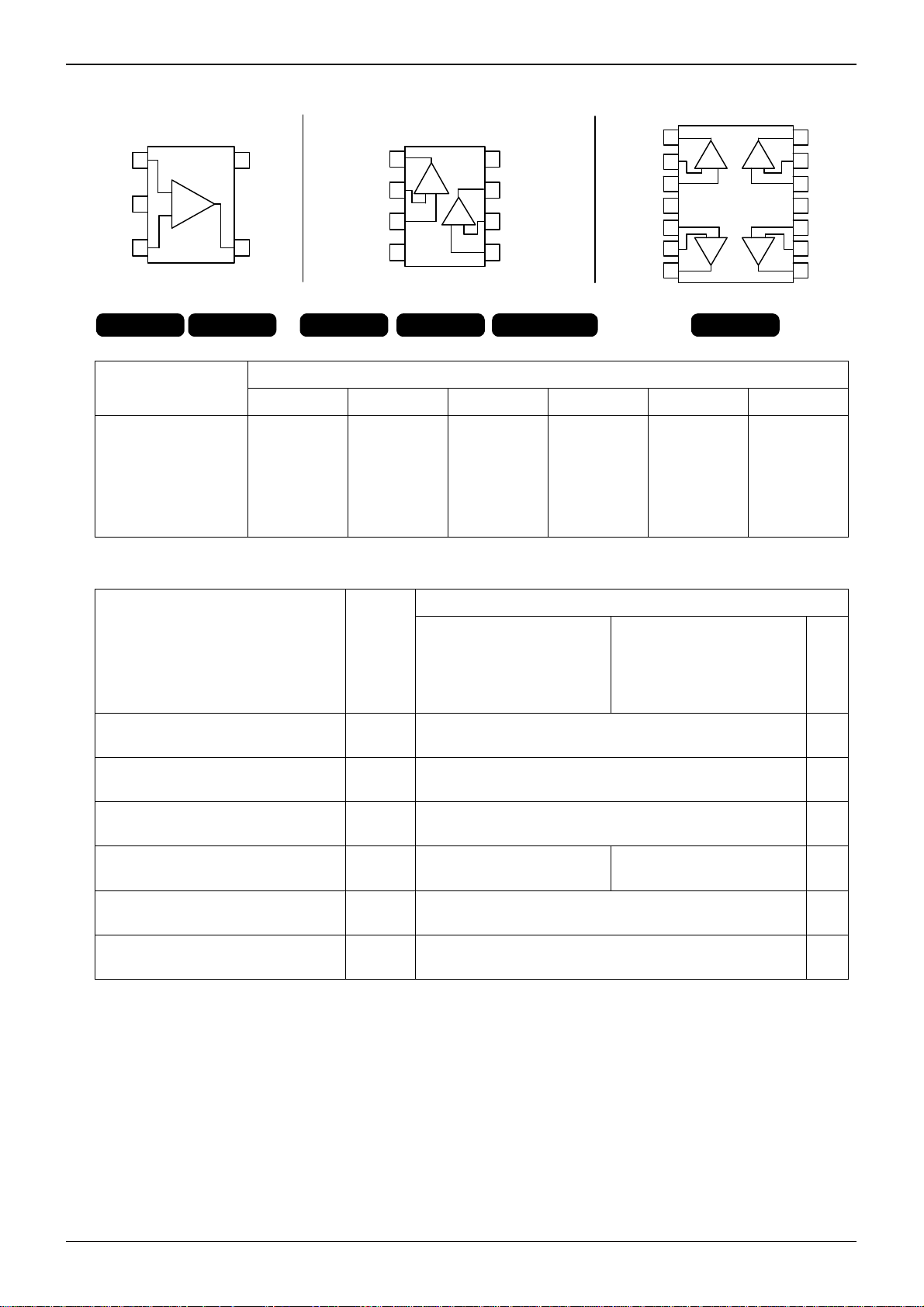
●Pin Assignments
IN+
VSS
+
2
-
51
VDD
OUT1
IN1-
IN1+
1
CH1
+
-
2
3
8
VDD
OUT2
7
CH2
-
6
+
IN2-
3 4
IN-
OUT
VSS
4
5
IN2+
1
OUT1
IN1-
2
IN1+
3
VDD
4
5
IN2+
6
IN2-
78
OUT2
SSOP5 HVSOF5 SOP8 MSOP8 VSON008X2030 SOP14
Package
Input type
SSOP5 HVSOF5 SOP8 VSON008X2030 MSOP8 SOP14
Technical Note
CH1
-
CH2
CH4
-
+
+
+-
-
+
CH3
14
13
12
11
10
9
OUT4
IN4-
IN4+
VSS
IN3+
IN3-
OUT3
Input-output Full Swing
BU7261G
BU7261SG
BU7241G
BU7241SG
BU7275HFV
BU7275SHFV
BU7295HFV
BU7295SHFV
BU7262F
BU7262SF
BU7242F
BU7242SF
BU7262NUX
BU7262SNUX
BU7242NUX
BU7242SNUX
BU7262FVM
BU7262SFVM
BU7242FVM
BU7242SFVM
BU7264F
BU7264SF
BU7244F
BU7244SF
●Absolute maximum rating (Ta=25[℃])
Ratings
Parameter Symbol
BU7261G, BU7241G,
BU7262F/FVM/NUX
BU7242F/FVM/NUX
BU7264F, BU7244F
BU7295HFV, BU7275HFV
BU7261SG, BU7241SG,
BU7262SF/FVM/NUX
BU7242SF/FVM/NUX
BU7264SF, BU7244SF
BU7295SHFV, BU7275SHFV
Unit
Supply Voltage VDD-VSS +7 V
Differential Input Voltage
(*1)
Vid VDD-VSS V
Input Common-mode Voltage Range Vicm (VSS-0.3)(VDD+0.3) V
Operating Temperature Topr -40 ~ +85 -40 ~ +105 ℃
Storage Temperature Tstg -55 ~ +125 ℃
Maximum Junction Temperature Tjmax +125 ℃
Note: Absolute maximum rating item indicates the condition which must not be exceeded.
Application of voltage in excess of absolute maximum rating or use out absolute maximum rated temperature environment
may cause deterioration of characteristics.
(*1) The voltage difference between inverting input and non-inverting input is the differential input voltage.
Then input terminal voltage is set to more than VSS.
www.rohm.com
© 2010 ROHM Co., Ltd. All rights reserved.
2/36
2010.12 - Rev.
Page 3
A
BU7261/BU7261S family, BU7241/BU7241S family, BU7295/BU7295S family, BU7275/BU7275S family
BU7262/BU7262S
family, BU7242/BU7242S family, BU7264/BU7264S family, BU7244/BU7244S family
●Electrical characteristics
○BU7261 family (Unless otherwise specified VDD=+3[V], VSS=0[V], Ta=25[℃])
Limits
Parameter
Symbol
Temperature
Range
BU7261G,
BU7261SG
Unit
Min. Typ. Max.
Input Offset Voltage
Input Offset Current
(*2)(*3)
Vio
(*2)
Iio 25℃ - 1 - pA
25℃ - 1 9
Full range - - 10
mV
Technical Note
Condition
VDD=1.8 ~ 5.5[V],
VOUT=VDD/2
-
Input Bias Current
Supply Current
(*2)
Ib 25℃ - 1 - pA
(*3)
IDD
25℃ - 250 550
Full range - - 600
RL=∞ All Op-Amps
μA
AV=0[dB], VIN=1.5[V]
-
High Level Output Voltage VOH 25℃ VDD-0.1 - - V RL=10[kΩ]
Low Level Output Voltage
VOL 25℃ - - VSS+0.1 V RL=10[kΩ]
Large Signal Voltage Gain AV 25℃ 70 95 - dB RL=10[kΩ]
Input Common-mode Voltage Range Vicm 25℃ 0 - 3 V VDD-VSS=3[V]
Common-mode Rejection Ratio CMRR 25℃ 45 60 - dB -
Power Supply Rejection Ratio PSRR 25℃ 60 80 - dB -
Output Source Current
Output Sink Current
(*4)
IOH 25℃ 4 10 - mA VDD-0.4[V]
(*4)
IOL 25℃ 5 12 - mA VSS+0.4[V]
Slew Rate SR 25℃ - 1.1 - V/μs CL=25[pF]
Gain Band width FT 25℃ - 2 - MHz CL=25[pF], AV=40[dB]
Phase Margin θ 25℃ - 50 - ° CL=25[pF], AV=40[dB]
(*2) Absolute value
(*3) Full range: BU7261: Ta=-40[℃] ~ +85[℃] BU7261S: Ta=-40[℃] ~ +105[℃]
(*4) Under the high temperature environment, consider the power dissipation of IC when selecting the output current.
When the terminal short circuits are continuously output, the output current is reduced to climb to the temperature inside IC.
www.rohm.com
© 2010 ROHM Co., Ltd. All rights reserved.
3/36
2010.12 - Rev.
Page 4

A
BU7261/BU7261S family, BU7241/BU7241S family, BU7295/BU7295S family, BU7275/BU7275S family
BU7262/BU7262S
family, BU7242/BU7242S family, BU7264/BU7264S family, BU7244/BU7244S family
○BU7262 family (Unless otherwise specified VDD=+3[V], VSS=0[V], Ta=25[℃])
Limits
Parameter
Symbol
Temperature
Range
BU7262F/FVM/NUX
BU7262S F/FVM/NUX
Unit
Min. Typ. Max.
Input Offset Voltage
Input Offset Current
(*5)(*6)
Vio
(*5)
Iio 25℃ - 1 - pA
25℃ - 1 9
Full range - - 10
mV
Technical Note
Condition
VDD=1.8 ~ 5.5[V]
VOUT=VDD/2
-
Input Bias Current
Supply Current
(*5)
Ib 25℃ - 1 - pA
(*6)
IDD
25℃ - 550 1100
Full range - - 1200
RL=∞ All Op-Amps
μA
AV=0[dB], VIN=1.5[V]
-
High Level Output Voltage VOH 25℃ VDD-0.1 - - V RL=10[kΩ]
Low Level Output Voltage VOL 25℃ - - VSS+0.1 V RL=10[kΩ]
Large Signal Voltage Gain AV 25℃ 70 95 - dB RL=10[kΩ]
Input Common-mode Voltage Range Vicm 25℃ 0 - 3 V VDD-VSS=3[V]
Common-mode Rejection Ratio CMRR 25℃ 45 60 - dB
Power Supply Rejection Ratio PSRR 25℃ 60 80 - dB
Output Source Current
Output Sink Current
(*7)
IOH 25℃ 4 10 - mA VDD-0.4[V]
(*7)
IOL 25℃ 5 12 - mA VSS+0.4[V]
-
-
Slew Rate SR 25℃ - 1.1 - V/μs CL=25[pF]
Gain Band width FT 25℃ - 2 - MHz CL=25[pF], AV=40[dB]
Phase Margin θ 25℃ - 50 - ° CL=25[pF], AV=40[dB]
Total Harmonic Distortion THD 25℃ - 0.05 - %
VOUT=0.8[Vp-p],
f=1[kHz]
Channel Separation CS 25℃ - 100 - dB AV=40[dB]
(*5) Absolute value
(*6) Full range: BU7262: Ta=-40[℃] ~ +85[℃] BU7262S: Ta=-40[℃] ~ +105[℃]
(*7) Under the high temperature environment, consider the power dissipation of IC when selecting the output current.
When the terminal short circuits are continuously output, the output current is reduced to climb to the temperature inside IC.
www.rohm.com
© 2010 ROHM Co., Ltd. All rights reserved.
4/36
2010.12 - Rev.
Page 5

A
BU7261/BU7261S family, BU7241/BU7241S family, BU7295/BU7295S family, BU7275/BU7275S family
BU7262/BU7262S
family, BU7242/BU7242S family, BU7264/BU7264S family, BU7244/BU7244S family
○BU7264 family (Unless otherwise specified VDD=+3[V], VSS=0[V], Ta=25[℃])
Limits
Parameter
Symbol
Temperature
Range
BU7264F
BU7264SF
Unit
Min. Typ. Max.
Input Offset Voltage
(*8)(*9)
Vio
25℃ - 1 9
Full range - - 10
mV
Technical Note
Condition
VDD=1.8 ~ 5.5[V]
VOUT=VDD/2
(*9)
(*8)
(*8)
Input Offset Current
Input Bias Current
Supply Current
High Level Output Voltage
Low Level Output Voltage
Large Signal Voltage Gain
Input Common-mode Voltage Range
Common-mode Rejection Ratio
Power Supply Rejection Ratio
(*10)
(*10)
Output Source Current
Output Sink Current
Iio 25℃ - 1 - pA
Ib 25℃ - 1 - pA
IDD
25℃ - 1100 2300
Full range - - 2800
VOH 25℃ VDD-0.1 - - V
VOL 25℃ - - VSS+0.1 V
AV 25℃ 70 95 - dB
Vicm 25℃ 0 - 3 V
RL=∞ All Op-Amps
μA
AV=0[dB], VIN=1.5[V]
RL=10[kΩ]
RL=10[kΩ]
RL=10[kΩ]
VDD-VSS=3[V]
CMRR 25℃ 45 60 - dB
PSRR 25℃ 60 80 - dB
IOH 25℃ 4 10 - mA
IOL 25℃ 5 12 - mA
VDD-0.4[V]
VSS+0.4[V]
-
-
-
-
Slew Rate
Gain Band width
Phase Margin
Total Harmonic Distortion
Channel Separation
(*8) Absolute value
(*9) Full range: BU7264: Ta=-40[℃] ~ +85[℃] BU7264S: Ta=-40[℃] ~ +105[℃]
(*10) Under the high temperature environment, consider the power dissipation of IC when selecting the output current.
When the terminal short circuits are continuously output, the output current is reduced to climb to the temperature inside IC.
SR 25℃ - 1.1 - V/μs
FT 25℃ - 2 - MHz
θ 25℃ - 50 -
THD 25℃ - 0.05 - %
CS 25℃ - 100 - dB
CL=25[pF]
CL=25[pF], AV=40[dB]
°
CL=25[pF], AV=40[dB]
VOUT=0.8[Vp-p],
f=1[kHz]
AV=40[dB]
www.rohm.com
© 2010 ROHM Co., Ltd. All rights reserved.
5/36
2010.12 - Rev.
Page 6

A
BU7261/BU7261S family, BU7241/BU7241S family, BU7295/BU7295S family, BU7275/BU7275S family
BU7262/BU7262S
family, BU7242/BU7242S family, BU7264/BU7264S family, BU7244/BU7244S family
○BU7295 family (Unless otherwise specified VDD=+3[V], VSS=0[V], Ta=25[℃])
Limits
Parameter
Symbol
Temperature
Range
BU7295HFV
BU7295SHFV
Unit
Min. Typ. Max.
Technical Note
Condition
(*12)
(*11)
(*11)
(*11)
Input Offset Voltage
Input Offset Current
Input Bias Current
Supply Current
High Level Output Voltage
Low Level Output Voltage
Large Signal Voltage Gain
Input Common-mode Voltage Range
Common-mode Rejection Ratio
Power Supply Rejection Ratio
Output Source Current
(*13)
Vio 25℃ - 1 6 mV
Iio 25℃ - 1 - pA
Ib 25℃ - 1 - pA
IDD
25℃ - 150 300
Full range - - 400
VOH 25℃ VDD-0.1 - - V
VOL 25℃ - - VSS+0.1 V
AV 25℃ 60 95 - dB
Vicm 25℃ 0 - 3 V
RL=∞ All Op-Amps
μA
AV=0[dB], VIN=1.5[V]
RL=10[kΩ]
RL=10[kΩ]
RL=10[kΩ]
VDD-VSS=3[V]
CMRR 25℃ 45 60 - dB
PSRR 25℃ 60 80 - dB
IOH 25℃ 4 8 - mA
VDD-0.4[V]
-
-
-
-
-
Output Sink Current
(*13)
Slew Rate
Gain Band width
Phase Margin
(*11) Absolute value
(*12) Full range: BU7295: Ta=-40[℃] ~ +85[℃] BU7295S: Ta=-40[℃] ~ +105[℃]
(*13) Under the high temperature environment, consider the power dissipation of IC when selecting the output current.
When the terminal short circuits are continuously output, the output current is reduced to climb to the temperature inside IC.
IOL 25℃ 9 18 - mA
SR 25℃ - 1.0 - V/μs
FT 25℃ - 1.0 - MHz
θ 25℃ - 60 - °
VSS+0.4[V]
CL=25[pF]
CL=25[pF], AV=40[dB]
CL=25[pF], AV=40[dB]
www.rohm.com
© 2010 ROHM Co., Ltd. All rights reserved.
6/36
2010.12 - Rev.
Page 7
A
BU7261/BU7261S family, BU7241/BU7241S family, BU7295/BU7295S family, BU7275/BU7275S family
BU7262/BU7262S
family, BU7242/BU7242S family, BU7264/BU7264S family, BU7244/BU7244S family
○BU7241 family (Unless otherwise specified VDD=+3[V], VSS=0[V], Ta=25[℃])
Limits
Parameter
Symbol
Temperature
Range
BU7241G,
BU7241SG
Unit
Min. Typ. Max.
Input Offset Voltage
(*14)(*15)
Vio
25℃ - 1 9
Full range - - 10
mV
Technical Note
Condition
VDD=1.8 ~ 5.5[V]
VOUT=VDD/2
(*15)
(*14)
(*14)
Input Offset Current
Input Offset Current
Supply Current
High Level Output Voltage
Low Level Output Voltage
Large Signal Voltage Gain
Input Common-mode Voltage Range
Common-mode Rejection Ratio
Power Supply Rejection Ratio
(*16)
(*16)
Output Source Current
Output Sink Current
Iio 25℃ - 1 - pA
Ib 25℃ - 1 - pA
IDD
25℃ - 70 150
Full range - - 250
VOH 25℃ VDD-0.1 - - V
VOL 25℃ - - VSS+0.1 V
AV 25℃ 70 95 - dB
Vicm 25℃ 0 - 3 V
RL=∞ All Op-Amps
μA
AV=0[dB], VIN=1.5[V]
RL=10[kΩ]
RL=10[kΩ]
RL=10[kΩ]
VDD-VSS=3[V]
CMRR 25℃ 45 60 - dB
PSRR 25℃ 60 80 - dB
IOH 25℃ 4 10 - mA
IOL 25℃ 5 12 - mA
VDD-0.4[V]
VSS+0.4[V]
-
-
-
-
Slew Rate
Gain Band width
Phase Margin
Total Harmonic Distortion
(*14) Absolute value
(*15) Full range: BU7241: Ta=-40[℃] ~ +85[℃] BU7241S: Ta=-40[℃] ~ +105[℃]
(*16) Under the high temperature environment, consider the power dissipation of IC when selecting the output current.
When the terminal short circuits are continuously output, the output current is reduced to climb to the temperature inside IC.
SR 25℃ - 0.4 - V/μs
FT 25℃ - 0.9 - MHz
θ 25℃ - 50 - °
THD 25℃ - 0.05 - %
CL=25[pF]
CL=25[pF], AV=40[dB]
CL=25[pF], AV=40[dB]
VOUT=0.8[Vp-p],
f=1[kHz]
www.rohm.com
© 2010 ROHM Co., Ltd. All rights reserved.
7/36
2010.12 - Rev.
Page 8

A
BU7261/BU7261S family, BU7241/BU7241S family, BU7295/BU7295S family, BU7275/BU7275S family
BU7262/BU7262S
family, BU7242/BU7242S family, BU7264/BU7264S family, BU7244/BU7244S family
○BU7242 family (Unless otherwise specified VDD=+3[V], VSS=0[V], Ta=25[℃])
Limits
Parameter
Symbol
Temperature
Range
BU7242F/FVM/NUX
BU7242S F/FVM/NUX
Unit
Min. Typ. Max.
Input Offset Voltage
(*17) (*18)
Vio
25℃ - 1 9
Full range - - 10
mV
Technical Note
Condition
VDD=1.8 ~ 5.5[V]
VOUT=VDD/2
(*18)
(*17)
(*17)
Input Offset Current
Input Bias Current
Supply Current
High Level Output Voltage
Low Level Output Voltage
Large Signal Voltage Gain
Input Common-mode Voltage Range
Common-mode Rejection Ratio
Power Supply Rejection Ratio
(*19)
(*19)
Output Source Current
Output Sink Current
Iio 25℃ - 1 - pA
Ib 25℃ - 1 - pA
IDD
25℃ - 180 360
Full range - - 600
VOH 25℃ VDD-0.1 - - V
VOL 25℃ - - VSS+0.1 V
AV 25℃ 70 95 - dB
Vicm 25℃ 0 - 3 V
RL=∞ All Op-Amps
μA
AV=0[dB], VIN=1.5[V]
RL=10[kΩ]
RL=10[kΩ]
RL=10[kΩ]
VDD-VSS=3[V]
CMRR 25℃ 45 60 - dB
PSRR 25℃ 60 80 - dB
IOH 25℃ 4 10 - mA
IOL 25℃ 5 12 - mA
VDD-0.4[V]
VSS+0.4[V]
-
-
-
-
Slew Rate
Gain Band width
Phase Margin
Total Harmonic Distortion
Channel Separation
(*17) Absolute value
(*18) Full range: BU7242: Ta=-40[℃] ~ +85[℃] BU7242S: Ta=-40[℃] ~ +105[℃]
(*19) Under the high temperature environment, consider the power dissipation of IC when selecting the output current.
When the terminal short circuits are continuously output, the output current is reduced to climb to the temperature inside IC.
SR 25℃ - 0.4 - V/μs
FT 25℃ - 0.9 - MHz
θ 25℃ - 50 - °
THD 25℃ - 0.05 - %
CS 25℃ - 100 - dB
CL=25[pF]
CL=25[pF], AV=40[dB]
CL=25[pF], AV=40[dB]
VOUT=0.8[Vp-p],
f=1[kHz]
AV=40[dB]
www.rohm.com
© 2010 ROHM Co., Ltd. All rights reserved.
8/36
2010.12 - Rev.
Page 9

A
BU7261/BU7261S family, BU7241/BU7241S family, BU7295/BU7295S family, BU7275/BU7275S family
BU7262/BU7262S
family, BU7242/BU7242S family, BU7264/BU7264S family, BU7244/BU7244S family
○BU7244 family (Unless otherwise specified VDD=+3[V], VSS=0[V], Ta=25[℃])
Limits
Parameter
Symbol
Temperature
Range
BU7244F
BU7244SF
Unit
Min. Typ. Max.
Input Offset Voltage
(*20) (*21)
Vio
25℃ - 1 9
Full range - - 10
mV
Technical Note
Condition
VDD=1.8 ~ 5.5[V]
VOUT=VDD/2
(*21)
(*20)
(*20)
Input Offset Current
Input Bias Current
Supply Current
High Level Output Voltage
Low Level Output Voltage
Large Signal Voltage Gain
Input Common-mode Voltage Range
Common-mode Rejection Ratio
Power Supply Rejection Ratio
(*22)
(*22)
Output Source Current
Output Sink Current
Iio 25℃ - 1 - pA
Ib 25℃ - 1 - pA
IDD
25℃ - 360 750
Full range - - 1200
VOH 25℃ VDD-0.1 - - V
VOL 25℃ - - VSS+0.1 V
AV 25℃ 70 95 - dB
Vicm 25℃ 0 - 3 V
RL=∞ All Op-Amps
μA
AV=0[dB], VIN=1.5[V]
RL=10[kΩ]
RL=10[kΩ]
RL=10[kΩ]
VDD-VSS=3[V]
CMRR 25℃ 45 60 - dB
PSRR 25℃ 60 80 - dB
IOH 25℃ 4 10 - mA
IOL 25℃ 5 12 - mA
VDD-0.4[V]
VSS+0.4[V]
-
-
-
-
Slew Rate
Gain Band width
Phase Margin
Total Harmonic Distortion
Channel Separation
(*20) Absolute value
(*21) Full range: BU7244: Ta=-40[℃] ~ +85[℃] BU7244S: Ta=-40[℃] ~ +105[℃]
(*22) Under the high temperature environment, consider the power dissipation of IC when selecting the output current.
When the terminal short circuits are continuously output, the output current is reduced to climb to the temperature inside IC.
SR 25℃ - 0.4 - V/μs
FT 25℃ - 0.9 - MHz
θ 25℃ - 50 - °
THD 25℃ - 0.05 - %
CS 25℃ - 100 - dB
CL=25[pF]
CL=25[pF], AV=40[dB]
CL=25[pF], AV=40[dB]
VOUT=0.8[Vp-p],
f=1[kHz]
AV=40[dB]
www.rohm.com
© 2010 ROHM Co., Ltd. All rights reserved.
9/36
2010.12 - Rev.
Page 10
A
BU7261/BU7261S family, BU7241/BU7241S family, BU7295/BU7295S family, BU7275/BU7275S family
BU7262/BU7262S
family, BU7242/BU7242S family, BU7264/BU7264S family, BU7244/BU7244S family
○BU7275 family (Unless otherwise specified VDD=+3[V], VSS=0[V], Ta=25[℃])
Limits
Parameter
Symbol
Temperature
Range
BU7275HFV
BU7275SHFV
Unit
Min. Typ. Max.
Technical Note
Condition
(*24)
(*23)
(*23)
(*23)
Input Offset Voltage
Input Offset Current
Input Bias Current
Supply Current
High Level Output Voltage
Low Level Output Voltage
Large Signal Voltage Gain
Input Common-mode Voltage Range
Common-mode Rejection Ratio
Power Supply Rejection Ratio
Output Source Current
(*25)
Vio 25℃ - 1 6 mV
Iio 25℃ - 1 - pA
Ib 25℃ - 1 - pA
IDD
25℃ - 40 80
Full range - - 130
VOH 25℃ VDD-0.1 - - V
VOL 25℃ - - VSS+0.1 V
AV 25℃ 60 95 - dB
Vicm 25℃ 0 - 3 V
RL=∞ All Op-Amps
μA
AV=0[dB], VIN=1.5[V]
RL=10[kΩ]
RL=10[kΩ]
RL=10[kΩ]
VDD-VSS=3[V]
CMRR 25℃ 45 60 - dB
PSRR 25℃ 60 80 - dB
IOH 25℃ 4 8 - mA
VDD-0.4[V]
-
-
-
-
-
Output Sink Current
(*25)
Slew Rate
Gain Band width
Phase Margin
(*23) Absolute value
(*24) Full range: BU7275: Ta=-40[℃] ~ +85[℃] BU7275S: Ta=-40[℃] ~ +105[℃]
(*25) Under the high temperature environment, consider the power dissipation of IC when selecting the output current.
When the terminal short circuits are continuously output, the output current is reduced to climb to the temperature inside IC.
IOL 25℃ 9 18 - mA
SR 25℃ - 0.3 - V/μs
FT 25℃ - 0.6 - MHz
θ 25℃ - 60 - °
VSS+0.4[V]
CL=25[pF]
CL=25[pF], AV=40[dB]
CL=25[pF], AV=40[dB]
www.rohm.com
© 2010 ROHM Co., Ltd. All rights reserved.
10/36
2010.12 - Rev.
Page 11
A
BU7261/BU7261S family, BU7241/BU7241S family, BU7295/BU7295S family, BU7275/BU7275S family
y
y
y
y
y
y
.
.
y
y
y
BU7262/BU7262S
family, BU7242/BU7242S family, BU7264/BU7264S family, BU7244/BU7244S family
Technical Note
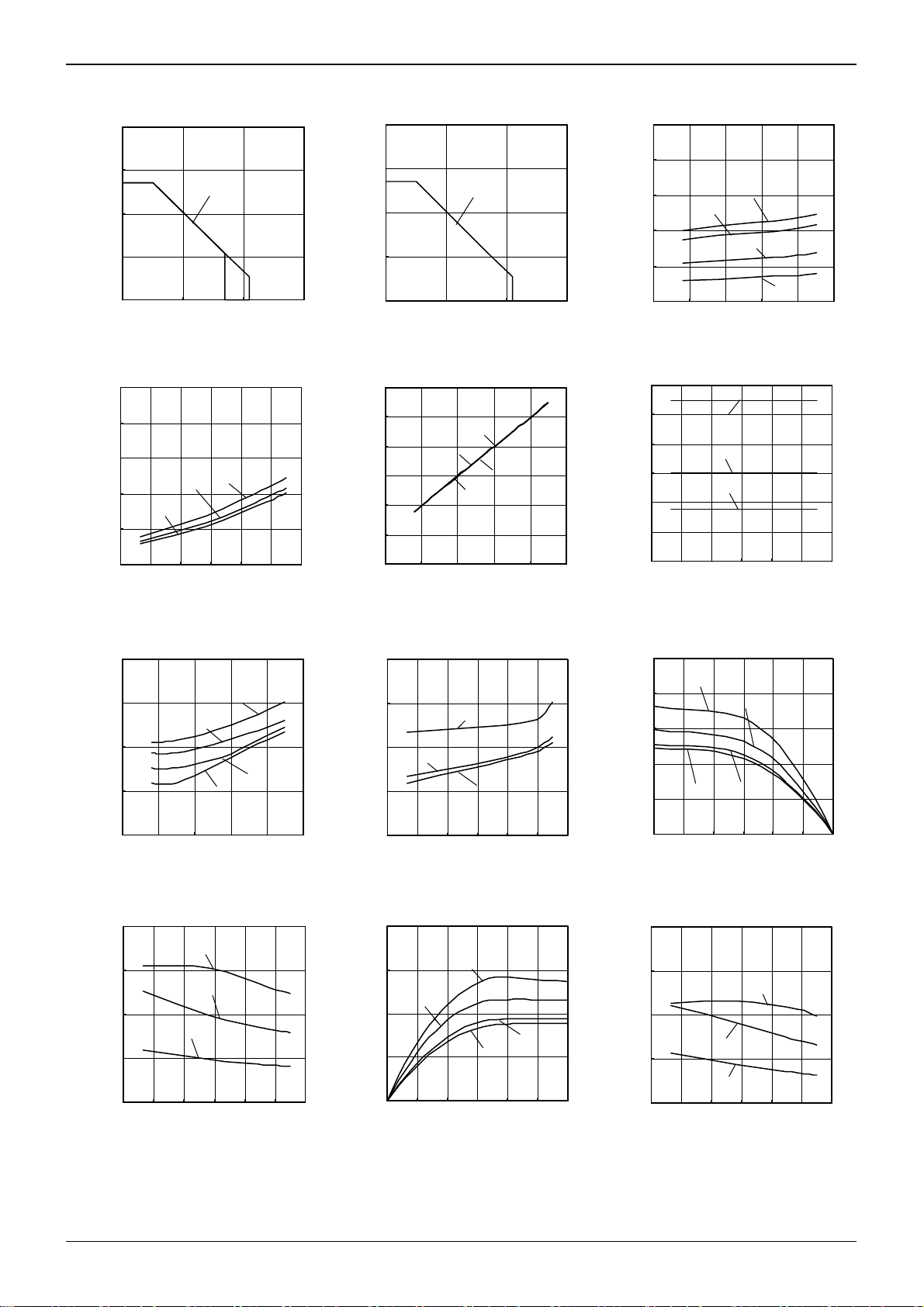
●Reference Data (BU7261 family)
800
600
400
200
POWER DISSIPATION [mW]
0
0 50 100 150
Fig.1 Fig.2 Fig.3
1000
800
600
400
SUPPLY CURRENT [μA]
200
0
-60 -30 0 30 60 90 120
Fig.4 Fig.5 Fig.6
Supply Current – Ambient Temperature
20
15
10
5
OUTPUT VOLTAGE LOW [mV]
0
123456
Fig.7 Fig.8 Fig.9
Output Voltage Low – Supply Voltage
20
15
10
5
OUTP UT SOURCE CURRE NT [ mA]
0
-60 -30 0 30 60 90 120
Fig.10 Fig.11 Fig.12
Output Source Current – Ambient Temperature
BU7261G
AMBIENT TEMPERATURE [℃]
Derating curve
3.0V
1.8V
AMBIENT TEMPERATURE [℃]
85℃
SUPPLY VOLTAGE [V]
(RL=10[kΩ])
5.5V
3.0V
1.8V
AMBIENT TEMPERATURE [℃]
(VOUT=VDD-0.4[V])
(*) The above data is ability value of sample, it is not guaranteed. BU7261G: -40[℃] ~ +85[℃] BU7261SG: -40[℃] ~ +105[℃]
-40℃
85
5.5V
BU7261 famil
BU7261 famil
105℃
25℃
BU7261 family
BU7261 family
800
600
BU7261SG
400
200
POWER DISSIPATION [mW]
0
0 50 100 150
AMBIENT TEMPERATURE [℃]
BU7261 famil
105
Derating curve
1.8V
105℃
25℃
BU7261 famil
BU7261 famil
]
℃
BU7261 famil
85℃
6
5
4
3
2
1
OUTPUT VOLTAGE HIGH [V]
0
123456
105℃
85℃
-40℃
SUPPLY VOLTAGE [V]
Output Voltage High – Supply Voltage
(RL=10[kΩ])
20
15
10
5
OUTPUT VOLTAGE LOW [mV]
0
-60 -30 0 30 60 90 120
5.5V
3.0V
AMBIENT TEMPERATURE [
Output Voltage Low – Ambient Temperature
(RL=10[kΩ])
80
60
40
20
OUTPUT S INK CUR RENT
0
0.0 0.5 1.0 1.5 2.0 2.5 3.0
-40℃
25℃
OUTPUT VOLTAGE [V]
Output Sink Current – Output Voltage
(VDD=3[V])
1000
800
600
400
SUPPLY CURRENT [µA]
200
0
123456
85℃
SUPPLY VOLTAGE [V]
BU7261 famil
105℃
25℃
-40℃
Supply Current – Supply Voltage
25℃
85℃
5.5V
BU7261 famil
]
℃
BU7261 family
BU7261 famil
6
5
4
3
2
1
OUTPUT VOLTAGE HIGH [V]
0
-60-300 306090120
5.5V
3.0V
1.8V
AMBIENT TEMPERATURE [
Output Voltage High – Ambient Temperature
(RL=10[kΩ])
50
40
30
20
10
OUTPUT SOURCE CURRENT [ mA]
0
-40℃
105℃
0 0.5 1 1.5 2 2.5 3
OUTPUT VOLTAGE [V]
Output Source Current – Output Voltage
(VDD=3[V])
40
30
20
10
OUTPUT S INK CURRENT [mA]
0
-60-300 306090120
3.0V
1.8V
AMBIENT TEMPERATURE [℃]
Output Sink Current – Ambient Temperature
(VOUT=VSS+0.4[V])
www.rohm.com
© 2010 ROHM Co., Ltd. All rights reserved.
11/36
2010.12 - Rev.
Page 12
A
BU7261/BU7261S family, BU7241/BU7241S family, BU7295/BU7295S family, BU7275/BU7275S family
y
y
y
y
y
y
y
y
y
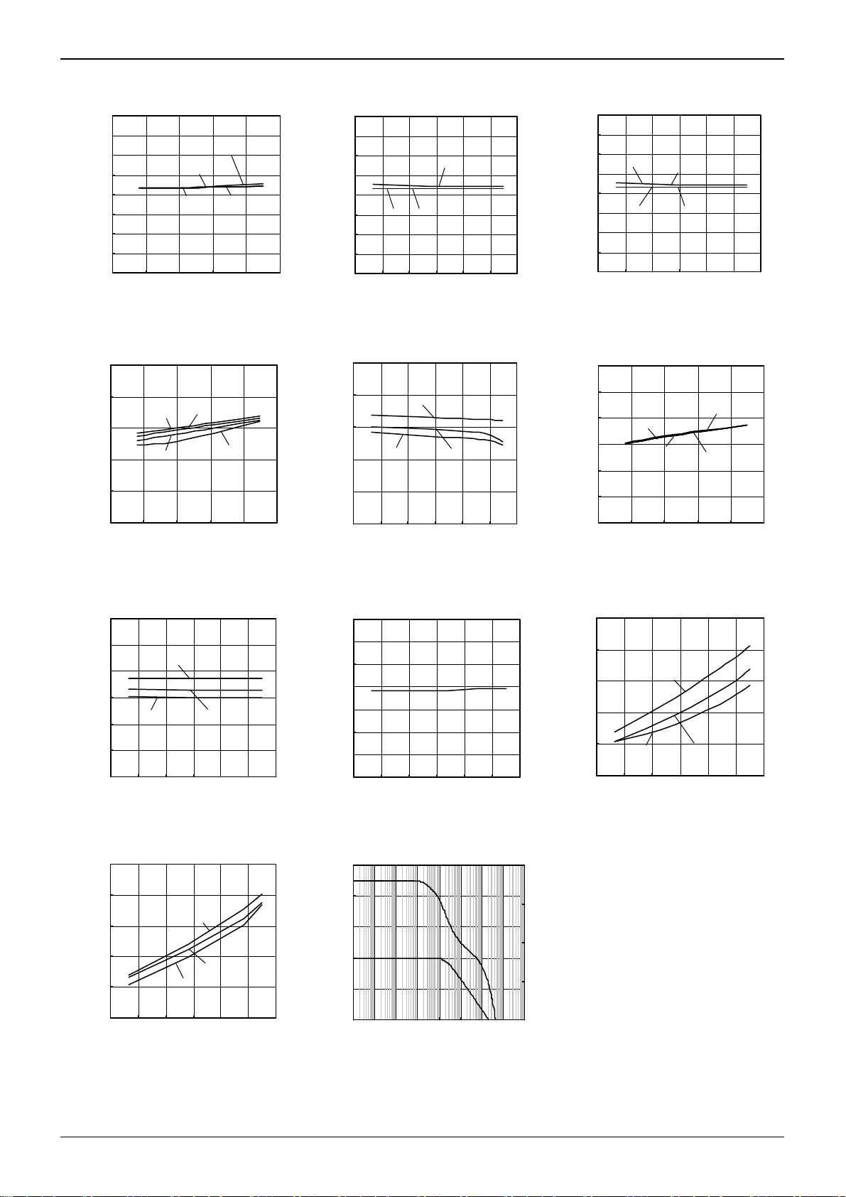
BU7262/BU7262S
10.0
7.5
5.0
2.5
0.0
-2.5
-5.0
-7.5
INPUT OFFSET VOLTAGE [mV]
-10.0
123456
Fig.13 Fig.14 Fig.15
Input Offset Voltage – Supply Voltage
(Vicm=VDD, VOUT=1.5[V])
160
140
120
100
80
LARGE SIGNAL VOLTAGE GAIN [dB]
60
123456
Fig.16 Fig.17 Fig.18
120
100
80
60
40
20
COMMON MODE RE J ECTION RATIO [dB]
0
-60 -30 0 30 60 90 120
Fig.19 Fig.20 Fig.21
Common Mode Rejection Ratio
2.5
2.0
1.5
1.0
SLEW RA T E H-L [V/μs]
0.5
0.0
-60 -30 0 30 60 90 120
Fig.22 Fig.23
Slew Rate H-L – Ambient Temperature
family, BU7242/BU7242S family, BU7264/BU7264S family, BU7244/BU7244S family
BU7261 famil
25℃
-40℃
105℃
SUPPLY VOLTAGE [V]
-40℃
85℃
SUPPLY VOLTAGE [V]
85℃
BU7261 famil
25℃
105℃
Large Signal Voltage Gain
– Supply Voltage
5.5V
1.8V
AMBIENT TEMPERATURE [
– Ambient Temperature
5.5V
1.8V
AMBIENT TEMPERATURE [℃]
3.0V
3.0V
BU7261 famil
]
℃
BU7261 family
10.0
7.5
5.0
2.5
0.0
INPUT OFFSET VOLTAGE [mV]
-2.5
-5.0
-7.5
-10.0
3.0V
1.8V
-60 -30 0 30 60 90 120
AMBIENT TEMPERATURE [℃]
Input Offset Voltage – Ambient Temperature
(Vicm=VDD, VOUT=1.5[V])
160
140
120
100
80
LARGE SIGNAL VOLTAGE GAIN [dB]
60
5.5V
-60 -30 0 30 60 90 120
AMBIENT TEMPERATURE [℃]
1.8V
Large Signal Voltage Gain
– Ambient Temperature
140
120
100
80
60
40
20
PO WER SUPPLY REJE CT ION RATIO [dB]
0
-60 -30 0 30 60 90 120
AMBIENT TEMPERATURE [℃]
Power Supply Rejection Ratio
– Ambient Temperature
100
80
60
GAIN[dB]
40
20
0
1.E+00 1.E+01 1.E+02 1.E+03 1.E+04 1.E+05 1.E+06 1.E+07 1.E+08
Phase
Gain
FREQUENCY [Hz]
Voltage Gain – Frequency
5.5V
3.0V
BU7261 famil
BU7261 famil
BU7261 famil
BU7261 famil
INPUT OFFSET VOLTAGE [mV]
Input Offset Voltage – Ambient Temperature
200
150
100
PHASE [deg]
50
0
10.0
7.5
5.0
2.5
0.0
-2.5
-5.0
-7.5
-10.0
-60 -30 0 30 60 90 120
AMBIENT TEMPERATURE [℃]
120
100
80
60
40
20
0
COMMON MODE REJECTION RAT IO [ dB]
123456
Common Mode Rejection Ratio
5
4
3
2
SLEW RATE L-H [V/µs]
1
0
-60 -30 0 30 60 90 120
AMBIENT TEMPERATURE [
Slew Rate L-H – Ambient Temperature
(*) The above data is ability value of sample, it is not guaranteed. BU7261G: -40[℃] ~ +85[℃] BU7261SG: -40[℃] ~ +105[℃]
Technical Note
85℃
-40℃
105℃
25℃
(VDD=3[V])
85℃
-40℃
SUPPLY VOLTAGE [V]
– Supply Voltage
5.5V
1.8V
3.0V
BU7261 family
BU7261 famil
105℃
25℃
BU7261 famil
]
℃
www.rohm.com
© 2010 ROHM Co., Ltd. All rights reserved.
12/36
2010.12 - Rev.
Page 13

A
BU7261/BU7261S family, BU7241/BU7241S family, BU7295/BU7295S family, BU7275/BU7275S family
.
.
y
y
y
y
y
y
y
y
y
BU7262/BU7262S
●Reference Data (BU7262 family)
1000
800
600
400
200
POWER DISSIPATION [mW]
0
050100150
Fig.24 Fig.25 Fig.26
1500
1200
900
600
SUPPLY CURRENT [ μA]
300
0
-60-30 0 30 60 90120
Fig.27 Fig.28 Fig.29
Supply Current – Ambient Temperature
20
15
10
5
OUTPUT VOLTAGE LOW [mV]
0
123456
Fig.30 Fig.31 Fig.32
Output Voltage Low – Supply Voltage
20
15
10
5
OUTP UT SOURCE CURRENT [mA]
0
-60 -30 0 30 60 90 120
Fig.33 Fig.34 Fig.35
Output Source Current – Ambient Temperature
family, BU7242/BU7242S family, BU7264/BU7264S family, BU7244/BU7244S family
BU7262SNUX
105
25℃
5.5V
3.0V
-40℃
105℃
85℃
BU7262 famil
SUPPLY CURRENT [µA]
BU7262 family
Output Voltage High – Ambient Temperature
BU7262 famil
BU7262 famil
Output Sink Current – Ambient Temperature
BU7262 famil
BU7262F
BU7262FVM
BU7262NUX
85
AMBIENT TEMPERATURE [℃]
Derating curve
BU7262 famil
5.5V
3.0V
1.8V
AMBIENT TEMPERATURE [℃]
105℃
85℃
25℃
-40℃
SUPPLY VOLTAGE [V]
(RL=10[kΩ])
5.5V
3.0V
1.8V
AMBIENT TEMPERATURE [℃]
(VOUT=VDD-0.4[V])
BU7262 family
BU7262 famil
1000
800
BU7262SF
600
400
200
POWER DISSIPATION [mW]
0
0 50 100 150
BU7262SFVM
AMBIENT TEMPERATURE [℃]
Derating curve
6
5
4
3
2
1
OUTPUT VOLTAGE HIGH [V]
0
123456
105℃
85℃
-40℃
SUPPLY VOLTAGE [V]
Output Voltage High – Supply Voltage
(RL=10[kΩ])
20
15
10
5
OUTPUT VOLTAGE LOW [mV]
0
-60 -30 0 30 60 90 120
1.8V
AMBIENT TEMPERATURE [℃]
Output Voltage Low – Ambient Temperature
(RL=10[kΩ])
80
60
25℃
40
20
OUTPUT SINK CURRENT [ mA]
0
0.0 0.5 1.0 1.5 2.0 2.5 3.0
OUTPUT VOLTAGE [V]
Output Sink Current – Output Voltage
(VDD=3[V])
2000
1600
1200
800
400
0
123456
Supply Current – Supply Voltage
6
5
4
3
2
1
OUTPUT VOLTAGE HIGH [V]
0
-60 -30 0 30 60 90 120
AMBIENT TEMPERATURE [℃]
50
40
30
20
10
OUTPUT SOURCE CURRENT [ mA]
0
00.511.522.53
Output Source Current – Output Voltage
40
30
20
10
OUTPUT SINK CURRENT [ mA]
0
-60 -30 0 30 60 90 120
(*)The above data is ability value of sample, it is not guaranteed. BU7262F/FVM/NUX: -40[℃] ~ +85[℃] BU7262S F/FVM/NUX: -40[℃] ~ +105[℃]
Technical Note
BU7262 famil
105℃
85℃
25℃
-40℃
SUPPLY VOLTAGE [V]
BU7262 family
5.5V
3.0V
1.8V
(RL=10[kΩ])
BU7262 famil
-40℃
25℃
85℃ 105℃
OUTPUT VOLTAGE [V]
(VDD=3.0[V])
BU7262 famil
5.5V
3.0V
1.8V
AMBIENT TEMPERATURE[℃]
(VOUT=VSS+0.4[V])
www.rohm.com
© 2010 ROHM Co., Ltd. All rights reserved.
13/36
2010.12 - Rev.
Page 14

A
BU7261/BU7261S family, BU7241/BU7241S family, BU7295/BU7295S family, BU7275/BU7275S family
y
y
y
y
y
y
y
y
y
y
y
BU7262/BU7262S
10.0
7.5
5.0
2.5
0.0
-2.5
-5.0
INPUT OFFSET VOLTAGE [mV]
-7.5
-10.0
123456
Fig.36 Fig.37 Fig.38
Input Offset Voltage – Supply Voltage
160
140
120
100
80
LARGE SIGNAL VOLTAGE GAIN [dB]
60
123456
Fig.39 Fig.40 Fig.41
120
100
80
60
40
20
COMMON MO DE REJ ECTION RATIO [dB]
0
-60 -30 0 30 60 90 120
Fig.42 Fig.43 Fig.44
2.5
2.0
1.5
1.0
SLEW RATE H-L [V/μs]
0.5
0.0
-60 -30 0 30 60 90 120
Fig.45 Fig.46
Slew Rate H-L – Ambient Temperature
family, BU7242/BU7242S family, BU7264/BU7264S family, BU7244/BU7244S family
1.8V
BU7262 famil
BU7262 famil
5.5V
BU7262 famil
BU7 mil
200
150
100
PHASE [deg]
50
0
BU7262 famil
105℃
25℃
85℃
-40℃
SUPPLY VOLTAGE[V]
(Vicm=VDD,VOUT=1.5[V])
BU7262 famil
105℃
85℃
25℃
-40℃
SUPPLY VOLTAGE [V]
Large Signal Voltage Gain
– Supply Voltage
5.5V
3.0V
AMBIENT TEMPERATURE [℃]
BU7262 famil
1.8V
Common Mode Rejection Ratio
– Ambient Temperature
BU7262 famil
5.5V
3.0V
1.8V
AMBIENT TEMPERATURE [℃]
10.0
7.5
5.0
2.5
0.0
-2.5
-5.0
INPUT OFFSET VOLTAGE [mV]
-7.5
-10.0
-60 -30 0 30 60 90 120
5.5V
3.0V
AMBIENT TEMPERATURE [℃]
Input Offset Voltage – Ambient Temperature
(Vicm=VDD, VOUT=1.5[V])
160
140
1.8V
120
100
80
LARGE SIGNAL VOLTAGE GAIN [dB]
60
-60 -30 0 30 60 90 120
3.0V
AMBIENT TEMPERATURE [℃]
Large Signal Voltage Gain
– Ambient Temperature
140
120
100
80
60
40
20
POWER SUPPLY REJECTION RATIO [dB]
0
-60 -30 0 30 60 90 120
AMBIENT TEMPERATURE [℃]
Power Supply Rejection Ratio
– Ambient Temperature
100
80
60
GAIN [dB]
40
20
0
1.E+00 1.E+01 1.E+02 1.E+03 1.E+04 1.E+05 1.E+06 1.E+07 1.E+08
Phase
Gain
FREQ UENCY [ Hz ]
Voltage Gain – Frequency
15
10
5
0
-5
-10
INPUT OFFSET VOLTAGE [mV]
-15
-101234
Input Offset Voltage – Input Voltage
120
100
80
60
40
20
0
COMMON MO D E REJECTION RAT I O [dB ]
123456
Common Mode Rejection Ratio
5
4
3
2
SLEW RATE L-H [V/μ s]
1
0
-60 -30 0 30 60 90 120
Slew Rate L-H – Ambient Temperature
(*)The above data is ability value of sample, it is not guaranteed. BU7262F/FVM/NUX: -40[℃] ~ +85[℃] BU7262S F/FVM/NUX: -40[℃] ~ +105[℃]
Technical Note
INPUT VOLTAGE [V]
(VDD=3[V])
-40℃
85℃
SUPPLY VOLTAGE [V]
– Supply Voltage
5.5V
1.8V
AMBIENT TEMPERATURE [℃]
85℃
25℃
BU7262 famil
-40℃
25℃
105℃
BU7262 famil
105℃
BU7262 famil
3.0V
www.rohm.com
© 2010 ROHM Co., Ltd. All rights reserved.
14/36
2010.12 - Rev.
Page 15

A
BU7261/BU7261S family, BU7241/BU7241S family, BU7295/BU7295S family, BU7275/BU7275S family
.
.
y
y
y
y
y
y
y
y
y
y
y
BU7262/BU7262S
●Reference Data (BU7264 family)
1000
800
600
400
200
POWER DISSIPATION [mW]
0
0 50 100 150
Fig.47 Fig.48 Fig.49
3000
2500
2000
1500
1000
SUPPLY CURRENT [ μA]
500
0
-60-30 0 30 60 90120
Fig.50 Fig.51 Fig.52
Supply Current – Ambient Temperature
15
10
5
OUTPUT VOLTAGE LOW [mV]
0
123456
Fig.53 Fig.54 Fig.55
Output Voltage Low – Supply Voltage
20
15
10
5
OUTPUT SOURCE CURRENT [ mA ]
0
-60 -30 0 30 60 90 120
Fig.56 Fig.57 Fig.58
Output Source Current – Ambient Temperature
family, BU7242/BU7242S family, BU7264/BU7264S family, BU7244/BU7244S family
5.5V
-40℃
85℃
25℃
BU7264 famil
105
BU7264 famil
BU7264 famil
BU7264 famil
105℃
3.0V
3000
2500
2000
1500
1000
SUPPLY CURRENT [µA]
500
OUTPUT VOLTAGE HIGH [V]
Output Voltage High – Ambient Temperature
OUTPUT S OURCE CU RRENT [ mA]
OUTPUT SINK CURRENT [mA]
Output Sink Current – Ambient Temperature
BU7264 famil
BU7264F
85
AMBIENT TEMPERATURE [℃]
Derating curve
BU7264 famil
5.5V
3.0V
1.8V
AMBIENT TEMPERATURE [℃]
BU7264 famil
85℃
SUPPLY VOLTAGE [V]
105℃
25℃
-40℃
(RL=10[kΩ])
BU7264 famil
5.5V
3.0V
1.8V
AMBIENT TEMPERATURE [
(VOUT=VDD-0.4[V])
1000
800
600
400
200
POWER DISSIPATION [mW]
0
0 50 100 150
BU7264SF
AMBIENT TEMPERATURE [℃]
Derating curve
6.0
5.0
4.0
3.0
2.0
1.0
OUTPUT VOLTAGE HIGH [V]
0.0
123456
105℃
85℃
-40℃
SUPPLY VOLTAGE [V]
Output Voltage High – Supply Voltage
(RL=10[kΩ])
15
10
1.8V
5
OUTPUT VOLTAGE LOW [mV]
0
-60 -30 0 30 60 90 120
AMBIENT TEMPERATURE [℃]
Output Voltage Low – Ambient Temperature
(RL=10[kΩ])
80
60
40
20
OUTPUT S INK CURRENT [mA]
0
]
℃
25℃
0.0 0.5 1.0 1.5 2.0 2.5 3.0
OUTPUT VOLTAGE [V]
Output Sink Current – Output Voltage
(VDD=3[V])
0
123456
Supply Current – Supply Voltage
6
5
4
3
2
1
0
-60 -30 0 30 60 90 120
AMBIENT TEMPERATURE [℃]
50
40
30
20
10
0
00.511.522.53
Output Source Current – Output Voltage
40
30
20
10
0
-60 -30 0 30 60 90 120
(*)The above data is ability value of sample, it is not guaranteed. BU7264F: -40[℃] ~ +85[℃] BU7264SF: -40[℃] ~ +105[℃]
Technical Note
BU7264 family
105℃
85℃
25℃
-40℃
SUPPLY VOLTAGE [V]
BU7264 famil
5.5V
3.0V
1.8V
(RL=10[kΩ])
-40℃
105℃
85℃
OUTPUT VOLTAGE [V]
(VDD=3[V])
3.0V
1.8V
AMBIENT TEMPERATURE[℃]
(VOUT=VSS+0.4[V])
BU7264 famil
25℃
BU7264 famil
5.5V
www.rohm.com
© 2010 ROHM Co., Ltd. All rights reserved.
15/36
2010.12 - Rev.
Page 16

A
BU7261/BU7261S family, BU7241/BU7241S family, BU7295/BU7295S family, BU7275/BU7275S family
y
y
y
y
y
y
y
y
BU7262/BU7262S
10.0
7.5
5.0
2.5
0.0
-2.5
-5.0
INPUT OFFSET VOLTAGE [mV]
-7.5
-10.0
123456
Fig.59 Fig.60 Fig.61
Input Offset Voltage – Supply Voltage
160
140
120
100
80
60
40
20
LARGE SIGNAL VOLTAGE GAIN [dB]
0
123456
Fig.62 Fig.63 Fig.64
120
100
80
60
40
20
0
COMMON MODE REJE CT ION RATIO [dB ]
-60 -30 0 30 60 90 120
Fig.65 Fig.66 Fig.67
Common Mode Rejection Ratio
3.0
2.5
2.0
1.5
1.0
SLEW RATE H-L [V/μs]
0.5
0.0
-60 -30 0 30 60 90 120
Fig.68 Fig.69
Slew Rate H-L – Ambient Temperature
(*)The above data is ability value of sample, it is not guaranteed. BU7264F: -40[℃] ~ +85[℃] BU7264SF: -40[℃] ~ +105[℃]
family, BU7242/BU7242S family, BU7264/BU7264S family, BU7244/BU7244S family
BU7264 famil
105℃
-40℃
INPUT VOLTAGE [V]
25℃
85℃
(Vicm=VDD,VOUT=1.5[V])
BU7264 famil
-40℃
85℃ 105℃
25℃
SUPPLY VOLTAGE [V]
Large Signal Voltage Gain
1.8V
5.5V
BU7264 family
3.0V
BU7264 famil
– Supply Voltage
5.5V
AMBIENT TEMPERATURE [℃]
– Ambient Temperature
1.8V
AMBIENT TEMPERATURE [℃]
3.0V
10.0
7.5
5.0
2.5
0.0
-2.5
-5.0
INPUT OFFSET VOLTAGE [mV]
-7.5
-10.0
-60 -30 0 30 60 90 120
5.5V
AMBIENT TEMPERATURE [
Input Offset Voltage – Ambient Temperature
(Vicm=VDD,VOUT=1.5[V])
160
140
120
100
80
LARGE SIGNAL VOLTAGE GAIN [dB]
60
1.8V 3.0V
-60 -30 0 30 60 90 120
AMBIENT TEMPERATURE [℃]
Large Signal Voltage Gain
– Ambient Temperature
140
120
100
80
60
40
20
POWER SUPPLY REJECTION RATIO [dB]
0
-60 -30 0 30 60 90 120
AMBIENT TEMPERATURE [
Power Supply Rejection Ratio
– Ambient Temperature
100
80
60
GAIN [dB]
40
20
0
1.E+00 1.E+01 1.E+02 1.E+03 1.E+04 1.E+05 1.E+06 1.E+07 1.E+08
Phase
Gain
FREQUENCY [Hz]
Voltage Gain – Frequency
3.0V
BU7264 famil
1.8V
]
℃
BU7264 family
5.5V
BU7264 famil
]
℃
BU7264 famil
200
150
100
PHASE [deg]
50
0
15
10
5
0
-40℃
25℃
INPUT VOLTAGE [V]
-5
-10
INPUT OFFSET VOLTAGE [mV]
-15
-1 0 1 2 3 4
Input Offset Voltage – Input Voltage
120
100
80
60
40
20
COMMON MODE REJECTION RATIO [dB]
0
123456
-40℃
85℃
SUPPLY VOLTAGE [V]
Common Mode Rejection Ratio
– Supply Voltage
5
4
3
2
SLEW RATE L-H [V/μ s]
1
0
-60 -30 0 30 60 90 120
1.8V
AMBIENT TEMPERATURE [℃]
Slew Rate L-H – Ambient Temperature
Technical Note
BU7264 family
25℃
105℃
BU7264 famil
105℃
BU7264 famil
3.0V
85℃
(VDD=3[V])
5.5V
www.rohm.com
© 2010 ROHM Co., Ltd. All rights reserved.
16/36
2010.12 - Rev.
Page 17

A
BU7261/BU7261S family, BU7241/BU7241S family, BU7295/BU7295S family, BU7275/BU7275S family
.
y
y
y
y
y
y
y
y
.
BU7262/BU7262S
●Reference Data (BU7295 family)
1000
800
600
400
200
POWER DISSIPATION [mW]
0
0 50 100 150
Fig.70 Fig.71 Fig.72
300
250
200
150
100
SUPPLY CURRENT [ μA]
50
0
-60-300 306090120
Fig.73 Fig.74 Fig.75
Supply Current – Ambient Temperature
15
10
5
OUTPUT VOLTAGE LOW [mV]
0
123456
Fig.76 Fig.77 Fig.78
Output Voltage Low – Supply Voltage
20
15
10
5
OUTPUT SOURCE CURRENT [ mA]
0
-60 -30 0 30 60 90 120
Fig.79 Fig.80 Fig.81
Output Source Current – Ambient Temperature
family, BU7242/BU7242S family, BU7264/BU7264S family, BU7244/BU7244S family
BU7295 famil
105
BU7295 famil
105℃
25℃
BU7295 famil
5.5V 3.0V
BU7295 famil
-40℃
105℃
85℃
BU7295HFV
85
AMBIENT TEMPERATURE [℃]
Derating curve
3.0V
AMBIENT TEMPERATURE [℃]
105℃
-40℃
85℃
25℃
SUPPLY VOLTAGE [V]
(RL=10[kΩ])
5.5V
3.0V
1.8V
AMBIENT TEMPERATURE [
(VOUT=VDD-0.4[V])
BU7295 famil
BU7295 family
5.5V
1.8V
BU7295 famil
BU7295 family
℃
1000
800
600
400
200
POWER DISSIPATION [mW]
0
0 50 100 150
AMBIENT TEMPERATURE [℃]
BU7295SHFV
Derating curve
6.0
5.0
4.0
3.0
2.0
1.0
OUTPUT VOLTAGE HIGH [V]
0.0
123456
85℃
-40℃
SUPPLY VOLTAGE [V]
Output Voltage High – Supply Voltage
(RL=10[kΩ])
15
10
1.8V
5
OUTPUT VOLTAGE LOW [mV]
0
-60 -30 0 30 60 90 120
AMBIENT TEMPERATURE [℃]
Output Voltage Low – Ambient Temperature
(RL=10[kΩ])
80
60
40
20
OUTPUT SINK CURRENT [ mA]
0
]
25℃
0.0 0.5 1.0 1.5 2.0 2.5 3.0
OUTPUT VOLTAGE [V]
Output Sink Current – Output Voltage
(VDD=3[V])
300
250
200
150
100
SUPPLY CURRENT [µA]
50
0
123456
Supply Current – Supply Voltage
6
5
4
3
2
1
OUTPUT VOLTAGE HIGH [V]
0
-60 -30 0 30 60 90 120
AMBIENT TEMPERATURE [℃]
Output Voltage High – Ambient Temperature
50
40
30
20
10
105℃
OUTP UT SOURCE CURRE NT [mA]
0
00.511.522.53
Output Source Current – Output Voltage
50
40
30
20
10
OUTPUT SINK CURRENT [mA]
0
-60 -30 0 30 60 90 120
Output Sink Current – Ambient Temperature
(*)The above data is ability value of sample, it is not guaranteed. BU7295HFV: -40[℃] ~ +85[℃] BU7295SHFV: -40[℃] ~ +105[℃]
Technical Note
BU7295 famil
85℃
25℃
SUPPLY VOLTAGE [V]
3.0V
1.8V
(RL=10[kΩ])
-40℃
85℃
OUTPUT VOLTAGE [V]
(VDD=3[V])
3.0V
1.8V
AMBIENT TEMPERATURE[℃]
(VOUT=VSS+0.4[V])
105℃
-40℃
BU7295 family
5.5V
BU7295 famil
25℃
BU7295 family
5.5V
www.rohm.com
© 2010 ROHM Co., Ltd. All rights reserved.
17/36
2010.12 - Rev.
Page 18

A
BU7261/BU7261S family, BU7241/BU7241S family, BU7295/BU7295S family, BU7275/BU7275S family
y
y
y
y
y
y
y
y
BU7262/BU7262S
10
8
6
4
2
0
-2
-4
-6
INPUT OFFSET VOLTAGE [mV]
-8
-10
123456
Fig.82 Fig.83 Fig.84
Input Offset Voltage – Supply Voltage
160
140
120
100
80
60
40
20
LARGE SIGNAL VOLTAGE GAIN [dB]
0
123456
Fig.85 Fig.86 Fig.87
120
100
80
60
40
20
COMMON MO DE REJ ECTION RAT IO [ dB ]
0
-60 -30 0 30 60 90 120
Fig.88 Fig.89 Fig.90
Common Mode Rejection Ratio
3.0
2.5
2.0
1.5
1.0
SLEW RA T E H-L [V/ μs]
0.5
0.0
-60 -30 0 30 60 90 120
Fig.91 Fig.92
Slew Rate H-L – Ambient Temperature
(*)The above data is ability value of sample, it is not guaranteed. BU7295HFV: -40[℃] ~ +85[℃] BU7295SHFV: -40[℃] ~ +105[℃]
family, BU7242/BU7242S family, BU7264/BU7264S family, BU7244/BU7244S family
BU7295 famil
105℃
-40℃
INPUT VOLTAGE [V]
25℃
85℃
(Vicm=VDD,VOUT=1.5[V])
BU7295 famil
-40℃
105℃
25℃
85℃
SUPPLY VOLTAGE [V]
Large Signal Voltage Gain
– Supply Voltage
5.5V
1.8V
AMBIENT TEMPERATURE [℃]
BU7295 famil
3.0V
– Ambient Temperature
BU7295 famil
3.0V
5.5V
1.8V
AMBIENT TEMPERATURE [℃]
10.0
7.5
INPUT OFFSET VOLTAGE [mV]
5.0
2.5
0.0
-2.5
-5.0
-7.5
-10.0
5.5V
3.0V
1.8V
-60 -30 0 30 60 90 120
AMBIENT TEMPERATURE [
]
℃
Input Offset Voltage – Ambient Temperature
(Vicm=VDD,VOUT=1.5[V])
160
140
120
100
80
LARGE SIGNAL VOLTAGE GAIN [dB]
60
-60 -30 0 30 60 90 120
3.0V
1.8V
AMBIENT TEMPERATURE [
BU7295 family
5.5V
]
℃
Large Signal Voltage Gain
– Ambient Temperature
140
120
100
80
60
40
20
PO WER SUPPLY REJ ECTI ON RATIO [d B]
0
-60 -30 0 30 60 90 120
AMBIENT TEMPERATURE [
BU7295 famil
]
℃
Power Supply Rejection Ratio
– Ambient Temperature
100
80
60
GAIN [dB]
40
20
0
1.E+00 1.E+01 1.E+02 1.E+03 1.E+04 1.E+05 1.E+06 1.E+07 1.E+08
Phase
Gain
FREQUENCY [Hz]
BU7295 famil
Voltage Gain – Frequency
200
150
100
PHASE [deg]
50
0
10
8
6
4
2
0
-2
-4
-6
INPUT OFFSET VOLTAGE [mV]
-8
-10
-101234
85℃ 105℃
INPUT VOLTAGE [V]
Input Offset Voltage – Input Voltage
(VDD=3[V])
120
100
80
60
40
20
COMMON MO DE RE J ECTI ON RATIO [dB]
0
123456
85℃
-40℃ 25℃
SUPPLY VOLTAGE [V]
Common Mode Rejection Ratio
– Supply Voltage
3.0
2.5
2.0
1.5
1.0
SLEW RATE L-H [V/µs]
0.5
0.0
5.5V
1.8V
-60 -30 0 30 60 90 120
AMBIENT TEMPERATURE [
Slew Rate L-H – Ambient Temperature
Technical Note
BU7295 familyBU7295 famil
-40℃
25℃
BU7295 famil
105℃
BU7295 family
3.0V
]
℃
www.rohm.com
© 2010 ROHM Co., Ltd. All rights reserved.
18/36
2010.12 - Rev.
Page 19

A
BU7261/BU7261S family, BU7241/BU7241S family, BU7295/BU7295S family, BU7275/BU7275S family
.
y
y
y
y
y
y
y
y
y
.
y
y
y
BU7262/BU7262S
family, BU7242/BU7242S family, BU7264/BU7264S family, BU7244/BU7244S family
Technical Note
●Reference Data (BU7241 family)
800
600
400
200
POWER DISSIPATION [mW]
0
0 50 100 150
AMBIENT TEMPERATURE [
Fig.93 Fig.94 Fig.95
250
200
150
100
SUPPLY CURRENT [ μA]
50
0
-60 -30 0 30 60 90 120
Fig.96 Fig.97 Fig.98
Supply Current – Ambient Temperature
60
50
40
30
20
10
OUTPUT VOLTAGE LOW [mV]
0
123456
Fig.99 Fig.100 Fig.101
Output Voltage Low – Supply Voltage
20
15
10
5
OUTPUT SOURCE CURRENT [mA]
0
-60 -30 0 30 60 90 120
AMBIENT TEMPERATURE [℃]
Fig.102 Fig.103 Fig.104
Output Source Current – Ambient Temperature
BU7241G
Derating curve
3.0V
SUPPLY VOLTAGE [V]
25℃
SUPPLY VOLTAGE [V]
(RL=10[kΩ])
5.5V
1.8V
(VOUT=VDD-0.4[V])
85
5.5V
85℃
1.8V
3.0V
BU7241 famil
℃
BU7241 famil
BU7241 famil
-40℃
105℃
BU7241 famil
800
600
400
200
POWER DISSIPATION [mW]
0
]
050100150
AMBIENT TEMPERATURE [℃]
BU7241SG
BU7241 famil
105
250
200
105℃
150
100
SUPPLY CURRENT [μA]
50
0
123456
85℃
25℃
-40℃
SUPPLY VOLTAGE [V]
Derating curve
6
5
4
3
2
1
OUTPUT VOL TAGE HIGH [V]
0
123456
105℃
85℃
-40℃
SUPPLY VOLTAGE [V]
BU7241 famil
25℃
Output Voltage High – Supply Voltage
(RL=10[kΩ])
60
50
40
30
20
10
OUTPUT VOLTAGE LOW [mV]
0
-60 -30 0 30 60 90 120
3.0V
1.8V
AMBIENT TEMPERATURE [℃]
BU7241 famil
5.5V
Output Voltage Low – Ambient Temperature
(RL=10[kΩ])
85℃
-40℃
BU7241 famil
25℃
105℃
80
70
60
50
40
30
20
OUTPUT SINK CURRENT [ mA]
10
0
0.0 0.5 1.0 1.5 2.0 2.5 3.0
OUTPUT VOLTAGE [V]
Output Sink Current – Output Voltage
(VDD=3[V])
Supply Current – Supply Voltage
6
5
4
3
2
1
OUTPUT VOLTAGE HIGH [V]
0
-60 -30 0 30 60 90 120
5.5V
3.0V
1.8V
AMBIENT TEMPERATURE [℃]
Output Voltage High – Ambient Temperature
(RL=10[kΩ])
50
40
-40℃
30
20
10
OUTP UT SOURCE CURRENT [mA]
0
00.511.522.53
25℃
85℃
105℃
OUTPUT VOLTAGE [V]
Output Source Current – Output Voltage
(VDD=3[V])
40
30
20
10
OUTPUT SINK CURRENT [ mA]
3.0V
1.8V
0
-60 -30 0 30 60 90 120
AMBIENT TEMPERATURE [℃]
Output Sink Current – Ambient Temperature
(VOUT=VSS+0.4[V])
(*)The above data is ability value of sample, it is not guaranteed. BU7241G: -40[℃] ~ +85[℃] BU7241SG: -40[℃] ~ +105[℃]
BU7241 famil
BU7241 famil
BU7241 famil
BU7241 famil
5.5V
www.rohm.com
© 2010 ROHM Co., Ltd. All rights reserved.
19/36
2010.12 - Rev.
Page 20

A
BU7261/BU7261S family, BU7241/BU7241S family, BU7295/BU7295S family, BU7275/BU7275S family
y
y
y
y
y
y
y
y
y
BU7262/BU7262S
10.0
7.5
5.0
2.5
0.0
-2.5
-5.0
INPUT OFFSET VOLTAGE [mV]
-7.5
-10.0
123456
Fig.105 Fig.106 Fig.107
Input Offset Voltage – Supply Voltage
160
140
120
100
80
LARGE SIGNAL VOLTAGE GAIN [dB]
60
123456
Fig.108 Fig.109 Fig.110
120
100
80
60
40
20
COMMO N MODE REJECTI ON RA T IO [d B]
0
-60 -30 0 30 60 90 120
Fig.111 Fig.112 Fig.113
Common Mode Rejection Ratio
2.0
1.5
1.0
0.5
SLEW RATE H-L [V/ μs]
0.0
-60 -30 0 30 60 90 120
Fig.114 Fig.115
Slew Rate H-L – Ambient Temperature
(*)The above data is ability value of sample, it is not guaranteed. BU7241G: -40[℃] ~ +85[℃] BU7241SG: -40[℃] ~ +105[℃]
family, BU7242/BU7242S family, BU7264/BU7264S family, BU7244/BU7244S family
3.0V
3.0V
BU7241 famil
]
℃
BU7241 family
BU7241 famil
BU7241 family
200
150
100
PHASE [deg]
50
0
BU7241 famil
25℃
105℃
SUPPLY VOLTAGE [V]
(Vicm=VDD, VOUT=1.5[V])
85℃
25℃
-40℃
SUPPLY VOLTAGE [V]
-40℃
85℃
BU7241 famil
105℃
Large Signal Voltage Gain
– Supply Voltage
5.5V
1.8V
AMBIENT TEMPERATURE [℃]
BU7241 famil
3.0V
– Ambient Temperature
BU7241 famil
5.5V
1.8V
AMBIENT TEMPERATURE [℃]
3.0V
10.0
7.5
5.0
2.5
0.0
-2.5
-5.0
INPUT OFFSET VOLTAGE [mV]
-7.5
-10.0
-60 -30 0 30 60 90 120
5.5V
1.8V
AMBIENT TEMPERATURE [
Input Offset Voltage – Ambient Temperature
(Vicm=VDD, VOUT=1.5[V])
160
140
120
100
80
LARGE SIGNAL VOLTAGE GAIN [dB]
60
5.5V
1.8V
-60 -30 0 30 60 90 120
AMBIENT TEMPERATURE [℃]
Large Signal Voltage Gain
– Ambient Temperature
150
120
90
60
30
PO WER SUPPLY REJE CT ION RATIO [dB]
0
-60 -30 0 30 60 90 120
AMBIENT TEMPERATURE [℃]
Power Supply Rejection Ratio
100
GAIN [dB]
– Ambient Temperature
Phase
80
60
40
20
0
1.E+00 1.E+01 1.E+02 1.E+03 1.E+04 1.E+05 1.E+06 1.E+07 1.E+08
Gain
FREQUENCY[Hz]
Voltage Gain – Frequency
15
10
5
0
-5
-10
INPUT OFFSET VOLTAGE [mV]
-15
-101234
85℃
-40℃
INPUT VOLTAGE [V]
Input Offset Voltage – Input Voltage
120
100
80
60
40
20
COMMON MO DE RE J ECTION RAT IO [dB]
0
123456
85℃
-40℃
SUPPLY VOLTAGE [V]
Common Mode Rejection Ratio
– Supply Voltage
3.0
2.5
2.0
1.5
1.0
SLEW RATE L-H [V/μs]
0.5
0.0
-60 -30 0 30 60 90 120
5.5V
1.8V
AMBIENT TEMPERATURE [℃]
Slew Rate L-H – Ambient Temperature
Technical Note
BU7241 famil
105℃
25℃
(VDD=3[V])
BU7241 famil
105℃
25℃
BU7241 famil
3.0V
www.rohm.com
© 2010 ROHM Co., Ltd. All rights reserved.
20/36
2010.12 - Rev.
Page 21

A
BU7261/BU7261S family, BU7241/BU7241S family, BU7295/BU7295S family, BU7275/BU7275S family
.
y
y
y
y
y
y
y
y
y
y
.
BU7262/BU7262S
●Reference Data (BU7242 family)
1000
800
600
400
200
POWER DISSIPATION [mW]
0
0 50 100 150
Fig.116 Fig.117 Fig.118
800
600
400
200
SUPPLY CURRENT [µA]
0
-60 -30 0 30 60 90 120
Fig.119 Fig.120 Fig.121
Supply Current – Ambient Temperature
60
50
40
30
20
10
OUTPUT VOLTAGE LOW [mV]
0
123456
Fig.122 Fig.123 Fig.124
Output Voltage Low – Supply Voltage
20
15
10
5
OUTPUT S OURCE CURRENT [ mA]
0
-60 -30 0 30 60 90 120
Fig.125 Fig.126 Fig.127
Output Source Current – Ambient Temperature
family, BU7242/BU7242S family, BU7264/BU7264S family, BU7244/BU7244S family
BU7242 famil
BU7242F
AMBIENT TEMPERATURE [℃]
BU7242FVM
BU7242NUX
3.0V
105℃
-40℃
85
BU7242 famil
5.5V
BU7242 famil
25℃
AMBIENT TEMPERATURE [℃]
Derating curve
1.8V
85℃
SUPPLY VOLTAGE [V]
(RL=10[kΩ])
BU7242 famil
5.5V
3.0V
1.8V
AMBIENT TEMPERATURE [
(VOUT=VDD-0.4[V])
1000
800
BU7242SF
600
400
200
POWER DISSIPATION [mW]
0
0 50 100 150
BU7242SFVM
AMBIENT TEMPERATURE [℃]
Derating curve
6
5
4
3
2
1
OUTPUT VOLTAGE HIGH [V]
0
123456
85℃
-40℃
SUPPLY VOLTAGE [V]
Output Voltage High – Supply Voltage
(RL=10[kΩ])
60
50
40
30
20
10
OUTPUT VOLTAGE LOW [mV]
0
-60 -30 0 30 60 90 120
3.0V
1.8V
AMBIENT TEMPERATURE [℃]
Output Voltage Low – Ambient Temperature
(RL=10[kΩ])
80
60
25℃
40
20
OUTPUT S INK CURRENT [ mA]
0
]
℃
0.00.51.01.52.02.53.0
OUTPUT VOLTAGE [V]
Output Sink Current – Output Voltage
(VDD=3[V])
-40℃
BU7242 famil
BU7242SNUX
105
BU7242 famil
105℃
25℃
BU7242 famil
5.5V
BU7242 famil
85℃
105℃
500
400
300
200
SUPPLY CURRENT [ µA]
100
OUTPUT VOLTAGE HIGH [V]
OUTP UT SOURCE CURRENT [mA]
OUTPUT S INK CUR RENT [ mA]
0
123456
Supply Current – Supply Voltage
6
5
4
3
2
1
0
-60 -30 0 30 60 90 120
AMBIENT TEMPERATURE [
Output Voltage High – Ambient Temperature
50
40
30
20
10
0
0 0.5 1 1.5 2 2.5 3
Output Source Current – Output Voltage
40
30
20
10
0
-60 -30 0 30 60 90 120
Output Sink Current – Ambient Temperature
(*)The above data is ability value of sample, it is not guaranteed. BU7242F/FVM/NUX: -40[℃] ~ +85[℃] BU7242S F/FVM/NUX: -40[℃] ~ +105[℃]
Technical Note
BU7242 famil
105℃
85℃
25℃
-40℃
SUPPLY VOLTAGE [V]
BU7242 family
5.5V
3.0V
1.8V
℃
(RL=10[kΩ])
BU7242 family
-40℃
25℃
85℃
105℃
OUTPUT VOLTAGE [V]
AMBIENT TEMPERATURE[℃]
(VOUT=VSS+0.4[V])
(VDD=3[V])
BU7242 famil
5.5V
3.0V
1.8V
]
www.rohm.com
© 2010 ROHM Co., Ltd. All rights reserved.
21/36
2010.12 - Rev.
Page 22

A
BU7261/BU7261S family, BU7241/BU7241S family, BU7295/BU7295S family, BU7275/BU7275S family
y
y
y
–
y
y
y
y
y
BU7262/BU7262S
10.0
7.5
5.0
2.5
0.0
-2.5
-5.0
-7.5
INPUT OFFSET VOLTAGE [mV]
-10.0
123456
Fig.128 Fig.129 Fig.130
Input Offset Voltage – Supply Voltage
160
140
120
100
80
LARGE SIGNAL VOLTAGE GAIN [dB]
60
123456
Fig.131 Fig.132 Fig.133
120
100
80
60
40
20
0
COMMON MO DE RE J ECTION RAT I O [dB ]
-60 -30 0 30 60 90 120
Fig.134 Fig.135 Fig.136
Common Mode Rejection Ratio
2.0
1.5
1.0
0.5
SLEW RATE H-L [V/µs]
0.0
-60 -30 0 30 60 90 120
Fig.137 Fig.138
Slew Rate H-L – Ambient Temperature
(*)The above data is ability value of sample, it is not guaranteed. BU7242F/FVM/NUX: -40[℃] ~ +85[℃] BU7242S F/FVM/NUX: -40[℃] ~ +105[℃]
family, BU7242/BU7242S family, BU7264/BU7264S family, BU7244/BU7244S family
1.8V
5.5V
BU7242 family
BU7242 family
BU7242 famil
BU7242 famil
200
150
100
PHASE [deg]
50
0
BU7242 famil
25℃
-40℃
85℃
SUPPLY VOLTAGE[V]
105℃
(Vicm=VDD, VOUT=1.5[V])
BU7242 family
105℃
85℃
25℃
SUPPLY VOLTAGE [V]
-40℃
Large Signal Voltage Gain
– Supply Voltage
AMBIENT TEMPERATURE [
BU7242 famil
5.5V
3.0V
1.8V
℃
– Ambient Temperature
AMBIENT TEMPERATURE [℃]
5.5V
1.8V
BU7242 famil
3.0V
10.0
7.5
5.0
2.5
0.0
-2.5
-5.0
INPUT OFFSET VOLTAGE [mV]
-7.5
-10.0
-60-30 0 30 60 90120
3.0V
1.8V
AMBIENT TEMPERATURE [℃]
Input Offset Voltage – Ambient Temperature
(Vicm=VDD, VOUT=1.5[V])
140
120
100
80
60
40
20
LARGE SIGNAL VOLTAGE GAIN [dB]
0
-60 -30 0 30 60 90 120
AMBIENT TEMPERATURE [℃]
Large Signal Voltage Gain
– Ambient Temperature
150
120
90
60
30
PO WER SUPPLY REJECTION RAT IO [dB]
0
]
-60 -30 0 30 60 90 120
AMBIENT TEMPERATURE [℃]
Power Supply Rejection Ratio
Ambient Temperature
100
80
60
GAIN [dB]
40
20
Phase
0
1.E+00 1.E+01 1.E+02 1.E+03 1.E+04 1.E+05 1.E+06 1.E+07 1.E+08
Voltage Gain – Frequency
3.0V
5.5V
Gain
FREQUENCY [Hz]
15
10
5
0
-5
-10
INPUT OFFSET VOLTAGE [mV]
-15
-101234
INPUT VOLTAGE [V]
Input Offset Voltage – Input Voltage
(VDD=3[V])
120
100
80
60
40
20
COMMON MO DE RE J ECTION RAT IO [ dB ]
0
25℃
123456
SUPPLY VOLTAGE [V]
Common Mode Rejection Ratio
– Supply Voltage
3.0
2.5
2.0
1.5
1.0
SLEW RATE L-H [V/µs]
0.5
0.0
-60 -30 0 30 60 90 120
5.5V
AMBIENT TEMPERATURE [℃]
Slew Rate L-H – Ambient Temperature
Technical Note
BU7242 famil
-40℃
25℃
85℃
105℃
BU7242 famil
85℃
105℃
-40℃
BU7242 famil
3.0V
1.8V
www.rohm.com
© 2010 ROHM Co., Ltd. All rights reserved.
22/36
2010.12 - Rev.
Page 23

A
BU7261/BU7261S family, BU7241/BU7241S family, BU7295/BU7295S family, BU7275/BU7275S family
.
y
y
y
y
y
y
y
y
y
y
.
BU7262/BU7262S
●Reference Data (BU7244 family)
1000
800
600
400
200
POWER DISSIPATION [mW]
0
0 50 100 150
Fig.139 Fig.140 Fig.141
1000
800
600
400
SUPPLY CURRENT [μA]
200
0
-60-30 0 30 60 90120
Fig.142 Fig.143 Fig.144
Supply Current – Supply Voltage
20
15
10
-40℃
5
OUTPUT VOLTAGE LOW [mV]
0
123456
Fig.145 Fig.146 Fig.147
Output Voltage Low – Supply Voltage
20
15
10
5
OUTPUT SOURCE CURRENT [ mA]
0
-60 -30 0 30 60 90 120
Fig.148 Fig.149 Fig.150
Output Source Current – Ambient Temperature
(*)The above data is ability value of sample, it is not guaranteed. BU7244F: -40[℃] ~ +85[℃] BU7244SF: -40[℃] ~ +105[℃]
family, BU7242/BU7242S family, BU7264/BU7264S family, BU7244/BU7244S family
BU7244 famil
BU7244F
85
AMBIENT TEMPERATURE [℃]
Derating curve
BU7244 family
5.5V
3.0V
1.8V
AMBIENT TEMPERATURE [℃]
BU7244 famil
85℃ 105℃
SUPPLY VOLTAGE [V]
(RL=10[kΩ])
BU7244 famil
5.5V
1.8V
AMBIENT TEMPERATURE [
3.0V
(VOUT=VDD-0.4[V])
25℃
℃
1000
800
600
400
200
POWER DISSIPATION [mW]
0
0 50 100 150
AMBIENT TEMPERATURE [℃]
BU7244 SF
Derating curve
6.00
5.00
105℃
4.00
3.00
2.00
1.00
OUTPUT VOLTAGE HIGH [V]
0.00
123456
85℃
-40℃
SUPPLY VOLTAGE [V]
Output Voltage High – Supply Voltage
(RL=10[kΩ])
20
15
10
5
OUTPUT VOLTAGE LOW [mV]
0
-60 -30 0 30 60 90 120
3.0V
1.8V
AMBIENT TEMPERATURE [℃]
Output Voltage Low – Ambient Temperature
(RL=10[kΩ])
80
60
40
20
OUTPUT SINK CURRENT [ mA]
0
0.0 0.5 1.0 1.5 2.0 2.5 3.0
]
25℃
OUTPUT VOLTAGE [V]
Output Sink Current – Output Voltage
(VDD=3[V])
5.5V
25℃
-40℃
BU7244 famil
105
BU7244 famil
BU7244 famil
BU7244 famil
85℃
105℃
1000
SUPPLY CURRENT [µA]
OUTPUT VOLTAGE HIGH [V]
Output Voltage High – Ambient Temperature
OUTP UT SOURCE CURRENT [mA]
OUTPUT SINK CURRENT [ mA]
Output Sink Current – Ambient Temperature
800
600
400
200
0
123456
Supply Current – Supply Voltage
8
6
4
2
0
-60 -30 0 30 60 90 120
AMBIENT TEMPERATURE [℃]
50
-40℃
40
30
20
105℃
10
0
00.511.522.53
Output Source Current – Output Voltage
40
30
20
10
0
-60 -30 0 30 60 90 120
Technical Note
BU7244 family
85℃
25℃
SUPPLY VOLTAGE [V]
5.5V
3.0V
1.8V
(RL=10[kΩ])
25℃
85℃
OUTPUT VOLTAGE [V]
(VDD=3[V])
5.5V
1.8V
AMBIENT TEMPERATURE[℃]
(VOUT=VSS+0.4[V])
105℃
-40℃
BU7244 famil
BU7244 famil
BU7244 famil
3.0V
www.rohm.com
© 2010 ROHM Co., Ltd. All rights reserved.
23/36
2010.12 - Rev.
Page 24

A
BU7261/BU7261S family, BU7241/BU7241S family, BU7295/BU7295S family, BU7275/BU7275S family
y
y
y
y
y
y
y
y
BU7262/BU7262S
10.0
7.5
5.0
2.5
0.0
-2.5
-5.0
INPUT OFFSET VOLTAGE [mV]
-7.5
-10.0
123456
Fig.151 Fig.152 Fig.153
Input Offset Voltage – Supply Voltage
160
140
120
100
80
60
40
20
LARGE SIGNAL VOLTAGE GAIN [dB]
0
123456
Fig.154 Fig.155 Fig.156
120
100
80
60
40
20
COMMON MO DE REJ ECTION RATIO [ dB ]
0
-60 -30 0 30 60 90 120
Fig.157 Fig.158 Fig.159
Common Mode Rejection Ratio
2.0
1.5
1.0
SLEW RA T E H-L [V/μs]
0.5
0.0
-60 -30 0 30 60 90 120
Fig.160 Fig.161
Slew Rate H-L – Ambient Temperature
family, BU7242/BU7242S family, BU7264/BU7264S family, BU7244/BU7244S family
BU7244 famil
25℃
105℃
-40℃
INPUT VOLTAGE [V]
85℃
(Vicm=VDD,VOUT=1.5[V])
BU7244 famil
85℃
25℃
-40℃
SUPPLY VOLTAGE [V]
105℃
Large Signal Voltage Gain
– Supply Voltage
5.5V
1.8V
AMBIENT TEMPERATURE [
BU7244 famil
3.0V
℃
– Ambient Temperature
BU7244 famil
3.0V
5.5V
1.8V
AMBIENT TEMPERATURE [℃]
10.0
7.5
5.0
2.5
0.0
-2.5
-5.0
INPUT OFFSET VOLTAGE [mV]
-7.5
-10.0
-60 -30 0 30 60 90 120
5.5V
1.8V
3.0V
AMBIENT TEMPERATURE [
Input Offset Voltage – Ambient Temperature
(Vicm=VDD,VOUT=1.5[V])
160
140
120
100
LARGE SIGNAL VOLTAGE GAIN [dB]
1.8V 3.0V
80
60
-60 -30 0 30 60 90 120
AMBIENT TEMPERATURE [
Large Signal Voltage Gain
– Ambient Temperature
140
120
100
80
60
40
20
POWER SUPPLY REJECTION RATIO [dB]
0
-60 -30 0 30 60 90 120
]
AMBIENT TEMPERATURE [
Power Supply Rejection Ratio
– Ambient Temperature
100
GAIN [dB]
Phase
80
60
Gain
40
20
0
1.E+00 1.E+01 1.E+02 1.E+03 1.E+04 1.E+05 1.E+06 1.E+07 1.E+08
FREQUENCY [Hz ]
Voltage Gain – Frequency
BU7244 famil
]
℃
BU7244 family
5.5V
]
℃
BU7244 famil
]
℃
BU7244 famil
200
150
100
PHASE [deg]
50
0
15
10
5
0
-5
-10
INPUT OFFSET VOLTAGE [mV]
-15
-101234
Input Offset Voltage – Input Voltage
120
100
80
-40℃
60
40
20
COMMON MO DE RE J ECTION RAT IO [dB]
0
123456
Common Mode Rejection Ratio
2.0
1.5
1.0
SLEW RATE L-H [V/µs]
0.5
0.0
-60 -30 0 30 60 90 120
Slew Rate L-H – Ambient Temperature
(*)The above data is ability value of sample, it is not guaranteed. BU7244F: -40[℃] ~ +85[℃] BU7244SF: -40[℃] ~ +105[℃]
Technical Note
25℃
85℃
INPUT VOLTAGE [V]
(VDD=3[V])
85℃
SUPPLY VOLTAGE [V]
– Supply Voltage
5.5V
AMBIENT TEMPERATURE[
1.8V
-40℃
105℃
25℃
BU7244 family
BU7244 family
105℃
BU7244 famil
3.0V
]
℃
www.rohm.com
© 2010 ROHM Co., Ltd. All rights reserved.
24/36
2010.12 - Rev.
Page 25

A
BU7261/BU7261S family, BU7241/BU7241S family, BU7295/BU7295S family, BU7275/BU7275S family
.
y
y
y
y
y
y
y
y
y
y
.
BU7262/BU7262S
●Reference Data (BU7275 family)
1000
800
600
400
200
POWER DISSIPATION [mW]
0
0 50 100 150
Fig.162 Fig.163 Fig.164
100
75
50
25
SUPPLY CURRENT [μA]
0
-60-300 306090120
Fig.165 Fig.166 Fig.167
Supply Current – Supply Voltage
15
10
5
OUTPUT VOLTAGE LOW [mV]
0
123456
Fig.168 Fig.169 Fig.170
Output Voltage Low – Supply Voltage
20
15
10
5
OUTPUT SOURCE CURRENT [ mA]
0
-60 -30 0 30 60 90 120
Fig.171 Fig.172 Fig.173
Output Source Current – Ambient Temperature
family, BU7242/BU7242S family, BU7264/BU7264S family, BU7244/BU7244S family
85℃
25℃
BU7275 famil
105
]
℃
BU7275 famil
BU7275 famil
BU7275 famil
105℃
100
75
50
25
SUPPLY CURRENT [µA]
8
6
4
2
OUTPUT VOLTAGE HIGH [V]
0
Output Voltage High – Ambient Temperature
50
40
30
20
10
OUTP UT SOURCE CURRENT [mA]
Output Source Current – Output Voltage
50
40
30
20
10
OUTP UT SINK CURRENT [mA]
Output Sink Current – Ambient Temperature
BU7275 famil
BU7275HFV
85
AMBIENT TEMPERATURE [℃]
Derating curve
BU7275 famil
3.0V
AMBIENT TEMPERATURE [
85℃
-40℃
SUPPLY VOLTAGE [V]
5.5V
1.8V
BU7275 famil
105℃
25℃
(RL=10[kΩ])
BU7275 famil
5.5V
3.0V
1.8V
AMBIENT TEMPERATURE [
(VOUT=VDD-0.4[V])
1000
800
600
400
200
POWER DISSIPATION [mW]
0
0 50 100 150
AMBIENT TEMPERATURE [
BU7275SHFV
Derating curve
6.00
5.00
105℃
4.00
3.00
2.00
1.00
OUTPUT VOLTAGE HIGH [V]
0.00
]
℃
123456
85℃
-40℃
SUPPLY VOLTAGE [V]
Output Voltage High – Supply Voltage
(RL=10[kΩ])
15
10
5.5V 3.0V
5
OUTPUT VOLTAGE LOW [mV]
0
-60 -30 0 30 60 90 120
1.8V
AMBIENT TEMPERATURE [℃]
Output Voltage Low – Ambient Temperature
(RL=10[kΩ])
80
-40℃
60
25℃
40
20
OUTPUT SINK CURRENT [ mA]
0
0.0 0.5 1.0 1.5 2.0 2.5 3.0
]
℃
OUTPUT VOLTAGE [V]
Output Sink Current – Output Voltage
(VDD=3[V])
0
123456
Supply Current – Supply Voltage
-60 -30 0 30 60 90 120
AMBIENT TEMPERATURE [℃]
105℃
0
00.511.522.53
0
-60 -30 0 30 60 90 120
AMBIENT TEMPERATURE[℃]
(*)The above data is ability value of sample, it is not guaranteed. BU7275 HFV: -40[℃] ~ +85[℃] BU7275S HFV: -40[℃] ~ +105[℃]
Technical Note
85℃
SUPPLY VOLTAGE [V]
5.5V
3.0V
1.8V
(RL=10[kΩ])
-40℃
85℃
OUTPUT VOLTAGE [V]
(VDD=3 [V])
1.8V
(VOUT=VSS+0.4[V])
105℃
-40℃ 25℃
25℃
5.5V
3.0V
BU7275 family
BU7275 family
BU7275 famil
BU7275 famil
www.rohm.com
© 2010 ROHM Co., Ltd. All rights reserved.
25/36
2010.12 - Rev.
Page 26

A
BU7261/BU7261S family, BU7241/BU7241S family, BU7295/BU7295S family, BU7275/BU7275S family
–
y
y
y
y
y
y
–
BU7262/BU7262S
10
8
6
4
2
0
-2
-4
-6
INPUT OFFSET VOLTAGE [mV]
-8
-10
123456
Fig.174 Fig.175 Fig.176
Input Offset Voltage – Supply Voltage
160
140
120
100
80
60
40
20
LARGE SIGNAL VOLTAGE GAIN [dB]
0
123456
Fig.177 Fig.178 Fig.179
120
100
80
60
40
20
COMMON MODE RE J ECTION RATIO [dB]
0
-60 -30 0 30 60 90 120
Fig.180 Fig.181 Fig.182
Common Mode Rejection Ratio
1.0
0.8
0.6
0.4
SLEW RA T E H-L [V/μs]
0.2
0.0
-60-300 306090120
Fig.183 Fig.184
Slew Rate H-L – Ambient Temperature
family, BU7242/BU7242S family, BU7264/BU7264S family, BU7244/BU7244S family
BU7275 famil
-40℃ 25℃
85℃
105℃
INPUT VOLTAGE [V]
(Vicm=VDD,VOUT=1.5[V])
BU7275 family
85℃
25℃
-40℃
SUPPLY VOLTAGE [V]
105℃
Large Signal Voltage Gain
– Supply Voltage
5.5V
AMBIENT TEMPERATURE[℃]
BU7275 family
3.0V
1.8V
– Ambient Temperature
BU7275 famil
5.5V
AMBIENT TEMPERATURE [℃]
3.0V
1.8V
10.0
7.5
INPUT OFFSET VOLTAGE [mV]
5.0
2.5
0.0
-2.5
-5.0
-7.5
-10.0
5.5V
3.0V
1.8V
-60 -30 0 30 60 90 120
AMBIENT TEMPERATURE [
]
℃
Input Offset Voltage – Ambient Temperature
(Vicm=VDD,VOUT=1.5[V])
160
140
120
100
80
LARGE SIGNAL VOLTAGE GAIN [dB]
60
-60 -30 0 30 60 90 120
3.0V
1.8V
AMBIENT TEMPERATURE [
BU7275 famil
5.5V
]
℃
Large Signal Voltage Gain
– Ambient Temperature
140
120
100
80
60
40
20
POWER SUPPLY REJECTION RATIO [dB]
0
-60 -30 0 30 60 90 120
AMBIENT TEMPERATURE [
BU7275 famil
]
℃
Power Supply Rejection Ratio
Ambient Temperature
100
Phase
80
60
GAIN [dB]
Gain
40
20
0
1.E+00 1.E+01 1.E+02 1.E+03 1.E+04 1.E+05 1.E+06 1.E+07 1.E+08
FREQUENCY [Hz]
Voltage Gain
BU7275 family
Frequency
200
150
100
PHASE [deg]
50
0
10
8
6
4
2
0
-2
-4
-6
INPUT OFFSET VOLTAGE [mV]
-8
-10
-101234
Input Offset Voltage – Input Voltage
120
100
80
60
40
20
COMMON MO DE RE J ECTION RAT IO [dB]
0
123456
Common Mode Rejection Ratio
1.0
0.8
s]
μ
0.6
0.4
SLEW RA T E L -H [ V/
0.2
0.0
-60 -30 0 30 60 90 120
Slew Rate L-H – Ambient Temperature
(*)The above data is ability value of sample, it is not guaranteed. BU7275HFV: -40[℃] ~ +85[℃] BU7275SHFV: -40[℃] ~ +105[℃]
Technical Note
25℃
85℃
INPUT VOLTAGE [V]
(VDD=3[V])
85℃
-40℃ 25℃
SUPPLY VOLTAGE [V]
– Supply Voltage
5.5V
AMBIENT TEMPERATURE [℃]
BU7275 familyBU7275 famil
-40℃
105℃
BU7275 family
105℃
BU7275 famil
3.0V
1.8V
www.rohm.com
© 2010 ROHM Co., Ltd. All rights reserved.
26/36
2010.12 - Rev.
Page 27

A
BU7261/BU7261S family, BU7241/BU7241S family, BU7295/BU7295S family, BU7275/BU7275S family
A
BU7262/BU7262S
family, BU7242/BU7242S family, BU7264/BU7264S family, BU7244/BU7244S family
Technical Note
●Test circuit 1 NULL method
VDD, VSS, EK, Vicm Unit: [V]
Parameter VF S1 S2 S3 VDD VSS EK Vicm Calculation
Input Offset Voltage VF1 ON ON OFF 3 0 -1.5 3 1
Large Signal V ol t age Gain
Common-mode Rejection Ratio
(Input Common-mode Voltage Range)
Power Supply Rejection Ratio
VF2
VF3 -2.5
VF4
VF5 3
VF6
VF7 5.5
ON ON ON 3 0
ON ON OFF 3 0 -1.5
ON ON OFF
1.8
0 -0.9 0 4
-0.5
1.5 2
0
-Calculation-
1. Input Offset Voltage (Vio)
Vio
=
|VF1|
1+Rf/Rs
[V]
2. Large Signal Voltage Gain (Av)
v
=
2×(1+Rf/Rs)
|VF2-VF3|
[dB]20Log
3. Common-mode Rejection Ratio (CMRR)
CMRR
=
20Log
1.8×(1+Rf/Rs)
|VF4-VF5|
[dB]
4. Power Supply Rejection Ratio (PSRR)
PSRR
=
20Log
3.7×(1+Rf/Rs)
|VF6-VF7|
[dB]
0.1[µF]
RS=50[Ω]
0.015[µF]
SW1
Ri=1[M
Ω]
0.015[µF]
Vicm
RS=50[Ω]
50[kΩ]
Ri=1[MΩ]
SW2
VDD
DUT
VSS
SW3
VRL
Rf=50[kΩ]
EK
Vo
500[k
1000[pF]
RL
500[k
Ω]
Ω]
0.01[µF]
15[V]
LL
VF
-15[V]
Fig.185 Test circuit 1 (one channel only)
3
www.rohm.com
© 2010 ROHM Co., Ltd. All rights reserved.
27/36
2010.12 - Rev.
Page 28

A
BU7261/BU7261S family, BU7241/BU7241S family, BU7295/BU7295S family, BU7275/BU7275S family
Δ
Δ
BU7262/BU7262S
family, BU7242/BU7242S family, BU7264/BU7264S family, BU7244/BU7244S family
●Test circuit2 switch condition
SW No.
SW 1 SW2 SW3 SW4 SW5 SW6 SW7 SW 8 SW 9 SW
Technical Note
10 SW11SW12
Supply Current
Maximum Output Volt age RL=10 [kΩ]
Output Current
Slew Rate
Maximum Frequency
OFF OFF ON OFF ON OFF OFF OFF OFF OFF OFF OFF
OFF ON OFF OFF ON OFF OFF ON OFF OFF ON OFF
OFF ON OFF OFF ON OFF OFF OFF OFF ON OFF OFF
OFF OFF ON OFF OFF OFF ON OFF ON OFF OFF ON
ON OFF OFF ON ON OFF OFF OFF ON OFF OFF ON
SW4
●
R2 100[kΩ]
VDD=3[V]
●
SW1
R1
1[kΩ]
SW2
SW5 SW6 SW7
-
+
GND
SW9 SW10 SW11SW8
CL
VIN-
VIN+
RL
Vo
Fig.186 Test circuit 2
3[V]
VIN
[V]
3[V]
VOUT
[V]
SR=ΔV /Δt
3[V
P-P
]
0[V]
0[V]
t
Input waveform Output waveform
Fig.187. Slew rate input output wave
SW12
V
t
t
www.rohm.com
© 2010 ROHM Co., Ltd. All rights reserved.
28/36
2010.12 - Rev.
Page 29

A
BU7261/BU7261S family, BU7241/BU7241S family, BU7295/BU7295S family, BU7275/BU7275S family
BU7262/BU7262S
family, BU7242/BU7242S family, BU7264/BU7264S family, BU7244/BU7244S family
●Test circuit 3 Channel separation
R2=100[kΩ]
R2=100[kΩ]
R1=1[kΩ]
VDD
R1=1[kΩ]
VDD
VOUT1
VIN
R1//R2
VSS
V
~
=1[Vrms]
R1//R2
VSS
CS=20Log
100×VOUT1
VOUT2
Fig.188 Test circuit 3
●Schematic diagram
VDD
Vbias
IN
+
IN
-
class
AB co ntr o l
OUT
VSS
Vbias
Fig.189 Simplified schematic
Technical Note
V
VOUT2
~
www.rohm.com
© 2010 ROHM Co., Ltd. All rights reserved.
29/36
2010.12 - Rev.
Page 30

A
BU7261/BU7261S family, BU7241/BU7241S family, BU7295/BU7295S family, BU7275/BU7275S family
BU7262/BU7262S
●Examples of circuit
○Voltage follower
○Inverting amplifier
Vin
○Non-inverting amplifier
family, BU7242/BU7242S family, BU7264/BU7264S family, BU7244/BU7244S family
Voltage gain is 0 [dB].
VDD
Vin
VSS
Fig. 190 Voltage follower circuit
R2
VDD
R1
R1//R2
Fig. 191 Inverting amplifier circuit
R1
Vin
Fig. 192 Non-inverting amplifier circuit
VSS
R2
VDD
VSS
Vout
Vout
This circuit controls output voltage (Vout) equal input
voltage (Vin), and keeps V out with stable because of high
input impedance and low output impedance.
Vout is shown next formula.
Vout=Vin
For inverting amplifier, Vin is amplified by voltage gain
decided R1 and R2, and phase reversed voltage is
outputted.
Vout is shown next formula.
Vout=-(R2/R1)・Vin
Input impedance is R1.
For non-inverting amplifier, Vin is amplified by voltage
gain decided R1 and R2, and phase is same with Vin.
Vout is shown next formula.
Vout=(1+R2/R1)・Vin
Vout
This circuit realizes high input impedance because Input
impedance is operational amplifier’s input Impedance.
Technical Note
www.rohm.com
© 2010 ROHM Co., Ltd. All rights reserved.
30/36
2010.12 - Rev.
Page 31

A
BU7261/BU7261S family, BU7241/BU7241S family, BU7295/BU7295S family, BU7275/BU7275S family
A
BU7262/BU7262S
●Examples of circuit
○Adder circuit
Vin1
Vin2
○Differential amplifier
Vin1
Vin2
family, BU7242/BU7242S family, BU7264/BU7264S family, BU7244/BU7244S family
R3
R1
R2
R1
R3
VDD
VSS
Fig. 193 Adder circuit
R2
VDD
R4
Fig. 194 Differential amplifier
VSS
Vout
Vout
dder circuit output the voltage that added up Input
voltage. A phase of the output voltage turns over,
because non-inverting circuit is used.
Vout is shown next formula.
Vout = -R3(Vin1/R1+Vin2/R2)
When three input voltage is as above, it connects
with input through resistance like R1 and R2.
Differential amplifier output the voltage
that amplified a difference of input voltage.
In the case of R1=R3=Ra, R2=R4=Rb
Vout is shown next formula.
Vout = -Rb/Ra(Vin1-Vin2)
Technical Note
www.rohm.com
© 2010 ROHM Co., Ltd. All rights reserved.
31/36
2010.12 - Rev.
Page 32

A
BU7261/BU7261S family, BU7241/BU7241S family, BU7295/BU7295S family, BU7275/BU7275S family
BU7262/BU7262S
●Description of electrical characteristics
Described here are the terms of electric characteristics used in this technical note. Items and symbols used are also shown.
Note that item name and symbol and their meaning may differ from those on another manufacture’s document or general document.
1. Absolute maximum ratings
Absolute maximum rating item indicates the condition which must not be exc eeded. Application of voltage in excess of
absolute maximum rating or use out of absolute maximum rated temp erature environment may cause deterioration of
dharacteristics.
1.1 Power supply voltage (VDD/VSS)
1.2 Differential input voltage (Vid)
1.3 Input common-mode voltage range (Vicm)
1.4 Power dissipation (Pd)
2. Electrical characteristics item
2.1 Input offset voltage (Vio)
2.2 Input offset current (Iio)
2.3 Input bias current (Ib)
2.4 Circuit current (IDD)
2.5 High level outp ut voltage / Low level outp ut voltage (VOM)
2.6 Large signal voltage gain (AV)
2.7 Input common-mode voltage range (Vicm)
2.8 Common-mode rejecti on ratio (CMRR)
2.9 Power supply rejection ratio (PSRR)
2.10 Channel separation (CS)
2.11 Slew rate (SR)
2.12 Unity gain frequency (ft)
2.13 Total harmonic distortion + Noise (THD+N)
2.14 Input referred noise voltage (Vn)
family, BU7242/BU7242S family, BU7264/BU7264S family, BU7244/BU7244S family
Indicates the maximum voltage that can be applied between the positive po wer supply terminal and negative po wer
supply terminalwithout deterioration or destruction of characteristics of internal circuit.
Indicates the maximum voltage that can be applied between non-inverting terminal and inverting ter minal without
deterioration and destruction of characteristics of IC.
Indicates the maximum voltage that can be applied to non-inverting terminal and inverting terminal without
deterioration or destruction of characteristics. Input common-mode voltage range of the maximum ratings not assure
normal operation of IC. When normalOperation of IC is desired, the input common-mode voltage of characteristics
item must be followed.
Indicates the power that can be consumed by specified mounted board at the ambient temperature 25℃(normal
temperature).
As for package product, Pd is determined by the temperature that can be permitted by IC chip in the package
(maximum junction temperature) and thermal resistance of the package.
Indicates the voltage difference between non-inverting terminal and inverting terminal. It can be translated into the
input voltage difference required for setting the output voltage at 0 [V].
Indicates the difference of input bias current between non-inverting terminal and inverting terminal.
Indicates the current that flows into or out of the input terminal. It is defined by the average of input bias current at
non-inverting terminal and input bias current at inverting terminal.
Indicates the IC current that flows under specified conditions and no-load steady status.
Indicates the voltage range that can be output by the IC und er specified load condition. It is typically divided into
high-level output voltage and low-level output voltage. High-level output voltage indicates the upper limit of output
voltage. Low-level output voltage indicates the lower limit.
Indicates the amplifying rate (gain) of output voltage against the voltage difference between non-inve rting terminal
and inverting terminal. It is normally the amplifying rate (gain) with reference to DC voltage.
Av = (Output voltage fluctuation) / (Input offset fluctuation)
Indicates the input voltage range where IC operates normally.
Indicates the ratio of fluctuation of input offset voltage when in-phase input voltage is changed. It is normall y the
fluctuation of DC.
CMRR =(Change of Input common-mode voltage)/(Input offset fluctuation)
Indicates the ratio of fluctuation of input offset voltage when supply voltage is changed. It is normally the fluctuation of DC.
PSRR=(Change of power supply voltage)/(Input offset fluctuation)
Indicates the fluctuation of input offset voltage or that of output voltage with reference to the change of output voltage
of driven channel.
Indicates the time fluctuation ratio of voltage output when step input signal is applied.
Indicates a frequency where the voltage gain of Op-Amp is 1.
Indicates the fluctuation of input offset voltage or that of output voltage with reference to the change of output voltage
of driven channel.
Indicates a noise voltage generated inside the operational amplifier equivalent by ideal voltage source connected in
series with input terminal.
Technical Note
www.rohm.com
© 2010 ROHM Co., Ltd. All rights reserved.
32/36
2010.12 - Rev.
Page 33

A
BU7261/BU7261S family, BU7241/BU7241S family, BU7295/BU7295S family, BU7275/BU7275S family
BU7262/BU7262S
family, BU7242/BU7242S family, BU7264/BU7264S family, BU7244/BU7244S family
Technical Note
●Derating curve
Power dissipation (total loss) indicates the power that can be consumed by IC at Ta=25℃(normal temperature).IC is heated
when it consumed power, and the temperature of IC ship becomes higher than ambient temperature. T he temperature that
can be accepted by IC chip depends on circuit configuration, manufacturing process, and co nsumable power is limited.
Power dissipation is determined by the temperature allowed in IC chip (maximum junction temperature) and thermal
resistance of package (heat dissipation capability). The maximum junction temperature is typically equal to the maximum
value in the storage temperature range. Heat generated by consumed power of IC radiates from the mold resin or lead frame
of the package. The parameter which indicates this heat dissipation capability (hardness of heat release) is called the rmal
resistance, represented by the symbol θj-a[℃/W]. The temperature of IC inside the package can be estimated by this
thermal resistance. Fig.195 (a) shows the model of thermal resistance of the package. Thermal resistance θja, ambient
temperature Ta, junction temperature Tj, and power dissipation Pd can be calculated by the equation below :
θja = (Tj-Ta) / Pd [℃/W] ・・・・・ (Ⅰ)
Derating curve in Fig.195(b) indicates power that can be consumed by IC with reference to ambient temperature. Power that
can be consumed by IC with reference to ambient temperature. Power that can be consumed by IC begins to attenuate at
certain ambient temperature. This gradient is determined by thermal resistance θja. Thermal resistance θja depends on chip
size, power consumption, package, ambient temperature, package condition, wind velocity, etc even when the same of
package is used. Thermal reduction curve indicates a reference value measured at a specifi ed condition. Fig196(c) ~ (h)
show a derating curve for an example of low voltage full swing
CMOS Op-Amp.
[W]
Pd(max)
θja = ( Tj ーTa ) / Pd [℃/W]
Ta [℃]
周囲温度
Ambient temperature Ta [℃]
P2
P1
θja1
θja2 <θja1
θja2
Tj(max)
0
1000
Chip surface temp er ature Tj [℃]
チップ表面温度
Power dissin]
消費電力 P [ W]
(a)Thermal resistance
800
600
400
200
POWER DISSIPATION [mW]
0
0 50 100 150
1000
800
AMBIENT TEMPERATURE[℃]
(c) BU7261G BU7241G
BU7275HFV BU7295HFV
540[mW]
600
540[mW]
535[mW]
85
535[mW]
Tj [℃]
Fig. 195 Thermal resistance and derating
BU7261G(*26)
BU7241G(*26)
BU7295HFV(*30)
BU7275HFV(*30)
BU7261SG(*26)
BU7241SG(*26)
BU7295SHFV(*30)
BU7275SHFV(*30)
1000
800
600
400
200
POWER DISSIPATION [mW]
0
0 50 100 150
AMBIENT TEMPERATURE[℃]
(d) BU7262F/FVM/NUX BU7242F/FVM/NUX
1000
800
600
620[mW]
480[mW]
412[mW]
620[mW]
480[mW]
412[mW]
400
200
POWER DISSIPATION [mW]
0
0 50 100 150
AMBIENT TEMPERATURE[℃]
(f) BU7261SG BU7241SG
BU7275SHFV BU7295SHFV
105
(*26) (*27) (*28)
5.4 6.2 4.8
400
200
POWER DISSIPATION [mW]
0
0 50 100 150
AMBIENT TEMPERATURE[℃]
(g) BU7262S F/FVM/NUX BU7242S F/FVM/NUX
(*29)
4.12
25 125
℃ ]
Ta[
Ambient temperature Ta [℃]
(b) Derating curve
BU7262F(*27)
BU7242F(*27)
BU7262FVM(*28)
BU7242FVM(*28)
BU7262NUX(*29)
BU7242NUX(*29)
85
BU7262SF(*27)
BU7242SF(*27)
BU7262SFVM(*28)
BU7242SFVM(*28)
BU7262SNUX(*29)
BU7242SNUX(*29)
105
(*30) (*31) Unit
5.35
When using the unit above Ta=25[℃], subtract the value above per degree[℃]. Permissible dissipation is the value.
when FR4 glass epoxy board 70[mm]×70[mm]×1.6[mm] (cooper foil area below 3[%]) is mounted.
75 100
1000
800
600
400
200
POWER DISSIPATION [mW]
50
BU7264F(*31)
BU7244F(*31)
488[mW]
0
0 50 100 150
AMBIENT TEMPERATURE[℃]
85
(e) BU7264F BU7244F
1000
800
600
400
200
POWER DISSIPATION [mW]
0
050100150
AMBIENT TEMPERATURE[℃]
488[mW]
BU7264SF(*31)
BU7244SF(*31)
105
(h) BU7264SF BU7244SF
4.88
[mW/℃]
Fig. 196 Derating Curve
www.rohm.com
© 2010 ROHM Co., Ltd. All rights reserved.
33/36
2010.12 - Rev.
Page 34

A
BU7261/BU7261S family, BU7241/BU7241S family, BU7295/BU7295S family, BU7275/BU7275S family
BU7262/BU7262S
●Notes for use
1) Absolute maximum ratings
Absolute maximum ratings are the values which indicate the limits, within which the given voltage range ca n be safely
charged to the terminal. However, it does not guarantee the circuit operation.
2) Applied voltage to the input terminal
For normal circuit operation of voltage comparator, please input voltage for its input terminal within input common mode
voltage VDD + 0.3[V].
Then, regardless of power supply voltage, VSS-0.3[V] can be applied to input terminals without deterioration or destruction
of its characteristics.
3) Operating power supply (split power supply/single power supply)
The voltage comparator operates if a given level of voltage is applied between VDD and VSS.
Therefore, the operational amplifier can be operated under single power supply or split power supply.
4) Power dissipation (pd)
If the IC is used under excessive power dissipation. An increase in the chip temperatur e will cause deterioration of the
radical characteristics of IC. For example, reduction of current capability. Take consideration of the effective power
dissipation and thermal design with a sufficient margin. Pd is reference to the provided power dissipation curve.
5) Short circuits between pins and incorrect mounting
Short circuits between pins and incorrect mounting when mounting the IC on a printed circuits board, take notice of the
direction and positioning of the IC.
If IC is mounted erroneously, It may be damaged. Also, when a foreign object is inserted between output, bet ween output
and VDD terminal or VSS terminal which causes short circuit, the IC may be damaged.
6) Using under strong electromagnetic field
Be careful when using the IC under strong electromagnetic field because it may malfunction.
7) Usage of IC
When stress is applied to the IC through warp of the printed circuit board, The characteristics may fluctuate due to the
piezo effect. Be careful of the warp of the printed circuit board.
8) Testing IC on the set board
When testing IC on the set board, in cases where the capacitor is connected to the low impedance, make sure to
discharge per fabrication because there is a possibility that IC may be damaged by stress.
When removing IC from the set board, it is essential to cut supply voltage. As a countermeasure against the static
electricity, observe proper grounding during fabrication process and take due care when carrying and storage it.
9) The IC destruction caused by capacitive load
The transistors in circuits may be damaged when VDD terminal and VSS terminal is shorted with the charged output
terminal capacitor.When IC is used as a operational amplifier or as an application circuit, where oscillation is not activated
by an output capacitor, the output capacitor must be kept below 0.1[μF] in order to prevent the damage mentioned above.
10) Decupling capacitor
Insert the decupling capacitance between VDD and VSS, for stable operation of operational amplifier.
11) Latch up
Be careful of input voltage that exceed the VDD and VSS. When CMOS device have sometimes occur latch up operation.
And protect the IC from abnormaly noise
12) Decupling capacitor
Insert the decupling capacitance between VDD and VSS, for stable operation of operational amplifier.
family, BU7242/BU7242S family, BU7264/BU7264S family, BU7244/BU7244S family
Technical Note
www.rohm.com
© 2010 ROHM Co., Ltd. All rights reserved.
34/36
2010.12 - Rev.
Page 35

A
BU7261/BU7261S family, BU7241/BU7241S family, BU7295/BU7295S family, BU7275/BU7275S family
BU7262/BU7262S
family, BU7242/BU7242S family, BU7264/BU7264S family, BU7244/BU7244S family
●Ordering part number
Technical Note
B U 7 2 6 2 S F V M
Part No. Part No.
SOP8
6.2±0.3
SOP14
6.2± 0.3
4.4± 0.2
1.5± 0.1
SSOP5
1.25Max.
・7261 7261S ・7264 7264S
・7241 7241S ・7244 7244S
・7262 7262S ・7295 7295S
・7242 7242S ・7275 7275S
5.0±0.2
(MAX 5.35 include BURR)
4.4±0.2
0.595
1.5±0.1
0.11
(MAX 9.05 include BURR)
14
1
1.27
0.11
+0.2
−0.1
2.8±0.2
1.6
1.1±0.05
0.05±0.05
7
6
1.27
8.7± 0.2
0.4± 0.1
2.9±0.2
5
12
0.95
438251
0.42±0.1
4
3
S
0.1 S
8
7
0.42
0.1 S
+
6
°
4
°
−4°
0.3MIN
+0.1
0.17
-
0.05
(Unit : mm)
0.15± 0.1
0.1
(Unit : mm)
°
+
6
°
4
°
−4
+0.05
0.13
−0.03
S
+0.05
−0.04
(Unit : mm)
0.3MIN
0.9±0.15
0.2Min.
Package
G : SSOP5
F : SOP8, SOP14
FVM : MSOP8
NUX : VSON008X2030
HFV : HVSOF5
<Tape and Reel information>
Quantity
Direction
of feed
<Tape and Reel information>
Quantity
Direction
of feed
<Tape and Reel information>
Quantity
Direction
of feed
-
T R
Packaging and forming specification
E2: Embossed tape and reel
(SOP8/SOP14)
TR: Embossed tape and reel
(SSOP5/MSOP8/VSON008X2030/HVSOF5)
Embossed carrier tapeTape
2500pcs
E2
The direction is the 1pin of product is at the upper left when you hold
()
reel on the left hand and you pull out the tape on the right hand
Reel
Embossed carrier tapeTape
2500pcs
E2
The direction is the 1pin of product is at the upper left when you hold
()
reel on the left hand and you pull out the tape on the right hand
Reel
Embossed carrier tapeTape
3000pcs
TR
The direction is the 1pin of product is at the upper right when you hold
()
reel on the left hand and you pull out the tape on the right hand
Reel
1pin
Order quantity needs to be multiple of the minimum quantity.
∗
1pin
Order quantity needs to be multiple of the minimum quantity.
∗
1pin
Order quantity needs to be multiple of the minimum quantity.
∗
Direction of feed
Direction of feed
Direction of feed
www.rohm.com
© 2010 ROHM Co., Ltd. All rights reserved.
35/36
2010.12 - Rev.
Page 36

A
BU7261/BU7261S family, BU7241/BU7241S family, BU7295/BU7295S family, BU7275/BU7275S family
BU7262/BU7262S
MSOP8
0.9MAX
family, BU7242/BU7242S family, BU7264/BU7264S family, BU7244/BU7244S family
2.9±0.1
(MAX 3.25 include BURR)
8
2.8±0.1
4.0±0.2
0.75±0.05
0.475
0.08±0.05
1
0.65
2
6
57
4
3
1PIN MARK
+0.05
0.22
−0.04
0.08 S
+
6°
4°
−4°
0.6±0.2
0.29±0.15
+0.05
0.145
−0.03
S
(Unit : mm)
<Tape and Reel information>
Embossed carrier tapeTape
Quantity
Direction
of feed
3000pcs
TR
The direction is the 1pin of product is at the upper right when you hold
()
reel on the left hand and you pull out the tape on the right hand
Reel
Order quantity needs to be multiple of the minimum quantity.
∗
1pin
HVSOF5
1.6±0.05
0.6MAX
1.2±0.05
+0.03
−0.02
0.02
(MAX 1.28 include BURR)
1.6±0.05
1.0±0.05
(0.05)
0.5
(0.8)
(0.3)
4
5
321
0.22±0.05
(0.91)
S
(0.41)
0.1 S
45
1
32
0.08
0.2MAX
0.13±0.05
M
(Unit : mm)
<Tape and Reel information>
Embossed carrier tapeTape
Quantity
Direction
of feed
3000pcs
TR
The direction is the 1pin of product is at the upper right when you hold
()
reel on the left hand and you pull out the tape on the right hand
Reel
1pin
Order quantity needs to be multiple of the minimum quantity.
∗
VSON008X2030
2.0±0.1
0.6MAX
0.08 S
C0.25
0.3±0.1
0.25
1.5±0.1
0.5
1PIN MARK
+0.03
4
518
+0.05
0.25
−0.04
3.0±0.1
−0.02
0.02
S
(0.12)
1.4±0.1
(Unit : mm)
<Tape and Reel information>
Embossed carrier tapeTape
Quantity
Direction
of feed
4000pcs
TR
The direction is the 1pin of product is at the upper right when you hold
()
reel on the left hand and you pull out the tape on the right hand
Reel
1pin
Order quantity needs to be multiple of the minimum quantity.
∗
Direction of feed
Technical Note
Direction of feed
Direction of feed
www.rohm.com
© 2010 ROHM Co., Ltd. All rights reserved.
36/36
2010.12 - Rev.
Page 37

Notes
No copying or reproduction of this document, in par t or in whole, is permitted without the
consent of ROHM Co.,Ltd.
The content specied herein is subject to change for improvement without notice.
The content specied herein is for the purpose of introducing ROHM's products (hereinafter
"Products"). If you wish to use any such Product, please be sure to refer to the specications,
which can be obtained from ROHM upon request.
Examples of application circuits, circuit constants and any other information contained herein
illustrate the standard usage and operations of the Products. The peripheral conditions must
be taken into account when designing circuits for mass production.
Great care was taken in ensuring the accuracy of the information specied in this document.
However, should you incur any damage arising from any inaccuracy or misprint of such
information, ROHM shall bear no responsibility for such damage.
The technical information specied herein is intended only to show the typical functions of and
examples of application circuits for the Products. ROHM does not grant you, explicitly or
implicitly, any license to use or exercise intellectual property or other rights held by ROHM and
other parties. ROHM shall bear no responsibility whatsoever for any dispute arising from the
use of such technical information.
Notice
The Products specied in this document are intended to be used with general-use electronic
equipment or devices (such as audio visual equipment, ofce-automation equipment, communication devices, electronic appliances and amusement devices).
The Products specied in this document are not designed to be radiation tolerant.
While ROHM always makes efforts to enhance the quality and reliability of its Products, a
Product may fail or malfunction for a variety of reasons.
Please be sure to implement in your equipment using the Products safety measures to guard
against the possibility of physical injury, re or any other damage caused in the event of the
failure of any Product, such as derating, redundancy, re control and fail-safe designs. ROHM
shall bear no responsibility whatsoever for your use of any Product outside of the prescribed
scope or not in accordance with the instruction manual.
The Products are not designed or manufactured to be used with any equipment, device or
system which requires an extremely high level of reliability the failure or malfunction of which
may result in a direct threat to human life or create a risk of human injur y (such as a medical
instrument, transportation equipment, aerospace machinery, nuclear-reactor controller, fuelcontroller or other safety device). ROHM shall bear no responsibility in any way for use of any
of the Products for the above special purposes. If a Product is intended to be used for any
such special purpose, please contact a ROHM sales representative before purchasing.
If you intend to export or ship overseas any Product or technology specied herein that may
be controlled under the Foreign Exchange and the Foreign Trade Law, you will be required to
obtain a license or permit under the Law.
Thank you for your accessing to ROHM product informations.
More detail product informations and catalogs are available, please contact us.
ROHM Customer Support System
www.rohm.com
© 2010 ROHM Co., Ltd. All rights reserved.
http://www.rohm.com/contact/
R1010
A
 Loading...