

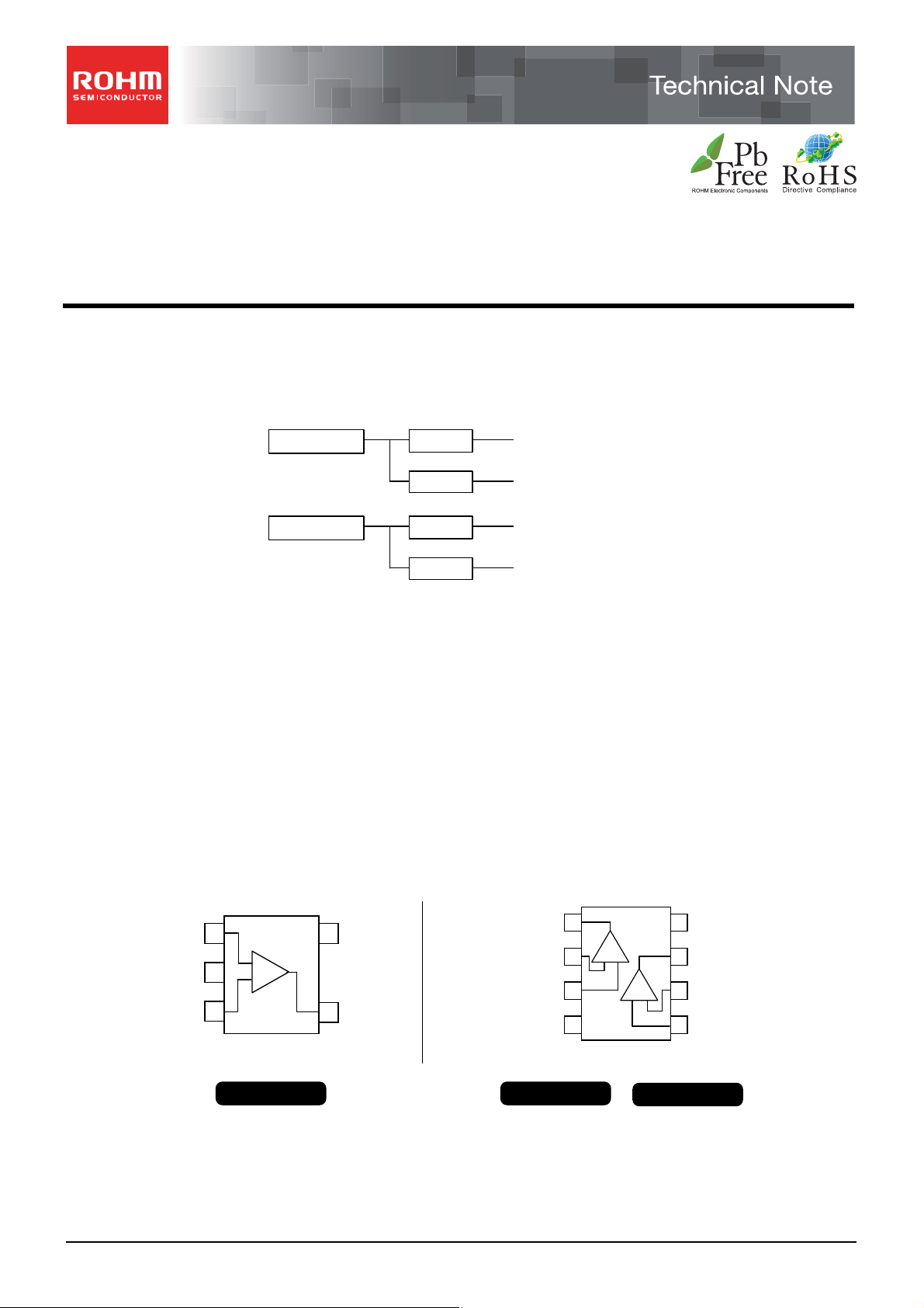
ROHM’s Selection Operational Amplifier/Comparator Series
Comparators:
Low Voltage CMOS
BU7251G,BU7251SG,BU7231G,BU7231SG,
BU7252F/FVM,BU7252S F/FVM,BU7232F/FVM,BU7232S F/FVM
●Description
CMOS comparator B U7 251/ B U 72 31f am i l y a nd BU7252/BU7232 family are input full swing and push pull o u tput compar a tor.
These ICs integrate one op-amp or two independent op-amps and phase compensation capacitor on a single chip.
The features of these ICs are low operating supplyVoltage that is +1.8V to +5.5V(single supply) and low supply current,
extremely low input bias current.
High speed
Single
Dual
Low power
Single
Dual
●Features
1) Low operating supply voltage (+1.8[V]~+5.5[V])
2) +1.8 [V]~+5.5[V](single supply)
±0.9[V]~±2.75[V](split supply)
3) Input and Output full swing
4) Push-pull output type
5) High speed operation (BU7251 family, BU7252 family)
6) Low supply current (BU7231 family, BU7232 family)
7) Internal ESD protection
Human body model (HBM) ±4000[V](Typ.)
8) Wide temperature range
-40[℃]~+85[℃] (BU7251G,BU7252 family, BU7231G, BU7232 family)
-40[℃]~+105[℃] (BU7251SG,BU7252S family, BU7231SG,BU7232S family)
● Pin Assignments
IN-
VSS
IN+
1
-
2
+
3
VDD
5
OUT
4
BU 7251G
BU 7251SG
BU 7231G
BU 7231SG
BU7251 G
(BU7251SG:105
BU7252 F/FVM
(BU7252S F/FVM:105
BU7231 G
(BU7231SG:105℃)
BU7232 F/FVM
(BU7232S F/FVM:105 ℃ )
OUT1
IN1-
IN1+
VSS
SOP8SSOP5
BU 7252F
BU 7252SF
BU 7232F
BU 7232SF
℃)
1
CH1
2
- +
3
4
℃)
CH2
+ -
VDD
8
OUT2
7
IN2-
6
5
IN2+
MSOP8
BU 7252FVM
BU 7252SFVM
BU 7232FVM
BU 7232SFVM
No.09049EAT06
www.rohm.com
© 2009 ROHM Co., Ltd. All rights reserved.
1/18
2009.05 - Rev.A
BU7251G,BU7251SG, BU7231G,BU7231SG,
BU7252F/FVM,BU7252S F/FVM,BU7232F/FVM,BU7232S F/FVM
Technical Note
●Absolute maximum ratings (Ta=25[℃])
Rating
Parameter Symbol
Supply Voltage VDD-VSS +7 V
Differential Input Voltage
(*1)
Vid VDD-VSS V
BU7251G,BU7252 F/FVM
BU7231G,BU7232 F/FVM
BU7251SG,BU7252S F/FVM
BU7231SG,BU7232S F/FVM
Input Common-mode voltage range Vicm (VSS-0.3) to VDD+0.3 V
Operating Temperature Topr -40 to+85 -40 to+105 ℃
Storage Temperature Tstg -55 to+125 ℃
Maximum junction Temperature Tjmax +125 ℃
Note Absolute maximum rating item indicates the condition which must not be exceeded.
Application of voltage in excess of absolute maximum rating or use out ab soluted maximum rated temperature environment may cause deterioration of characteri stics.
(*1) The voltage difference between inverting input and non-inverting input is the differential input voltage.Then input terminal voltage is set to more then VEE.
●Electrical characteristics
○BU7251 family (Unless otherwise specified VDD=+3[V], VSS=0[V], Ta=25[℃])
Parameter Symbol
(*2)
(*2)(*4)
(*2)
Input Offset Voltage
Input Offset Current
Input Bias Current
Input Common-mode voltage Range
Large Signal Voltage Gain
Supply current
Power supply rejection ratio
Common-mode rejection ratio
Output source current
Output sink current
High Level Output Voltage
Low Level Output Voltage
(*4)
PSRR 25℃
CMRR 25℃
(*3)
(*3)
(*4)
(*4)
Output rise time
Output fall time
Propagation delay L to H
Propagation delay H to L
(*2) Abusolute values
(*3) Reference to power dissipation under the high temperature environment and decide the output current.
Continuous short circuit is occurring the degenerate of output current characteristics.
(*4) Full range BU7251:Ta=-40[℃] to +85[℃] BU7251S:Ta=-40[℃] to +105[℃]
TPLH 25℃
TPHL 25℃
T emperature
range
Vio 25℃
Iio 25℃
Ib 25℃
Vicm 25℃
AV 25℃
IDD
25℃
full range - - 50
IOH 25℃
IOL 25℃
VOH 25℃
VOL 25℃
Tr 25℃
Tf 25℃
Guaranteed Limit
BU7251G,BU7251SG
Unit Condition
Min. Typ. Max.
- 1 11
- 1 -
- 1 -
mV -
pA pA -
0 - 3
- 90 -
- 15 35
- 80 -
- 80 1 2 3 6 -
dB RL=10[kΩ]
μA RL=∞
dB -
dB mA VDD-0.4
mA VSS+0.4
VDD-0.1 - -
- - VSS+0.1
- 50 -
- 20 -
- 0.55 -
μs CL=15pF 100mV over drive
- 0.25 -
V (VDD-VSS)=3[V]
V RL=10[kΩ]
V RL=10[kΩ]
ns CL=15pF 100mV over drive
ns CL=15pF 100mV over drive
μs CL=15pF 100mV over drive
○BU7252 family (Unless otherwise specified VDD=+3[V], VSS=0[V], Ta=25[℃])
Guaranteed Limit
Parameter Symbol
(*2)
(*2)(*4)
(*2)
Input Offset Voltage
Input Offset Current
Input Bias Current
Input Common-mode voltage Range
Large Signal Voltage Gain
Supply current
Power supply rejection ratio
Common-mode rejection ratio
Output source current
Output sink current
High Level Output Voltage
Low Level Output Voltage
(*4)
PSRR 25℃
CMRR 25℃
(*3)
(*3)
(*4)
(*4)
Output rise time
Output fall time
Propagation delay L to H
Propagation delay H to L
(*2) Abusolute values
(*3) Reference to power dissipation under the high temperature environment and decide the output current.
Continuous short circuit is occurring the degenerate of output current characteristics.
(*4) Full range BU7251,BU7252:Ta=-40[℃] to +85[℃] BU7251S,BU7252S:Ta=-40[℃] to +105[℃]
TPLH 25℃
TPHL 25℃
T emperature
range
Vio 25℃
Iio 25℃
Ib 25℃
Vicm 25℃
AV 25℃
IDD
25℃
full range - - 80
IOH 25℃
IOL 25℃
VOH 25℃
VOL 25℃
Tr 25℃
Tf 25℃
BU7252 F/FVM
BU7252S F/FVM
Unit Condition
Min. Typ. Max.
- 1 11
- 1 -
- 1 -
mV -
pA pA -
0 - 3
- 90 -
- 35 65
- 80 -
- 80 1 2 3 6 -
dB RL=10[kΩ]
μA RL=∞
dB -
dB mA VDD-0.4
mA VSS+0.4
VDD-0.1 - -
- - VSS+0.1
- 50 -
- 20 -
- 0.55 -
μs CL=15pF 100mV over drive
- 0.25 -
V (VDD-VSS)=3[V]
V RL=10[kΩ]
V RL=10[kΩ]
ns CL=15pF 100mV over drive
ns CL=15pF 100mV over drive
μs CL=15pF 100mV over drive
Unit
2/18
BU7251G,BU7251SG, BU7231G,BU7231SG,
BU7252F/FVM,BU7252S F/FVM,BU7232F/FVM,BU7232S F/FVM
Technical Note
○BU7231 family (Unless otherwise specified VDD=+3[V], VSS=0[V], Ta=25[℃])
Guaranteed Limit
Parameter Symbol
T emperature
range
BU7231G,BU7231SG
Unit Condition
Min. Typ. Max.
Input Offset Voltage
Input Offset Current
Input Bias Current
(*5)
Vio 25℃ - 1 11 mV -
(*5)
Iio 25℃ - 1 - pA -
(*5)
Ib 25℃ - 1 - pA Input Common-mode voltage Range Vicm 25℃ 0 - 3 V (VDD-VSS)=3[V]
Large Signal Voltage Gain AV 25℃ - 90 - dB RL=10[kΩ]
Supply current IDD
25℃ - 5 15
full range - - 30
μA RL=∞
Power supply rejection ratio PSRR 25℃ - 80 - dB -
Common-mode rejection ratio CMRR 25℃ - 80 - dB -
Output source current
Output sink current
High Level Output Voltage
Low Level Output Voltage
(*6)
IOH 25℃ 1 2 - mA VDD-0.4
(*6)
IOL 25℃ 3 6 - mA VSS+0.4
(*7)
VOH 25℃ VDD-0.1 - - V RL=10[kΩ]
(*7)
VOL 25℃ - - VSS+0.1 V RL=10[kΩ]
Output rise time Tr 25℃ - 50 - ns CL=15pF 100mV over drive
Output fall time Tf 25℃ - 20 - ns CL=15pF 100mV over drive
Propagation delay L to H TPLH 25℃ - 1.7 - μs CL=15pF 100mV over drive
Propagation delay H to L TPHL 25℃ - 0.5 - mV CL=15pF 100mV over drive
(*5) Abusolute values
(*6) Reference to power dissipation under the high temperature environment and decide the output current.
Continuous short circuit is occurring the degenerate of output current characteristics.
(*7) Full range BU7231:Ta=-40[℃] to +85[℃] BU7231S,BU7232S:Ta=-40[℃] to +105[℃]
○BU7232 family (Unless otherwise specified VDD=+3[V], VSS=0[V], Ta=25[℃])
Guaranteed Limit
Parameter Symbol
T emperature
range
BU7232F/FVM
BU7232S F/FVM
Unit Condition
Min. Typ. Max.
Input Offset Voltage
Input Offset Current
Input Bias Current
(*5)
Vio 25℃ - 1 11 mV -
(*5)
Iio 25℃ - 1 - pA -
(*5)
Ib 25℃ - 1 - pA Input Common-mode voltage Range Vicm 25℃ 0 - 3 V (VDD-VSS)=3[V]
Large Signal Voltage Gain AV 25℃ - 90 - dB RL=10[kΩ]
Supply current IDD
25℃ - 10 25
full range - - 50
μA RL=∞
Power supply rejection ratio PSRR 25℃ - 80 - dB -
Common-mode rejection ratio CMRR 25℃ - 80 - dB -
Output source current
Output sink current
High Level Output Voltage
Low Level Output Voltage
(*6)
IOH 25℃ 1 2 - mA VDD-0.4
(*6)
IOL 25℃ 3 6 - mA VSS+0.4
(*7)
VOH 25℃ VDD-0.1 - - V RL=10[kΩ]
(*7)
VOL 25℃ - - VSS+0.1 V RL=10[kΩ]
Output rise time Tr 25℃ - 50 - ns CL=15pF 100mV over drive
Output fall time Tf 25℃ - 20 - ns CL=15pF 100mV over drive
Propagation delay L to H TPLH 25℃ - 1.7 - μs CL=15pF 100mV over drive
Propagation delay H to L TPHL 25℃ - 0.5 - mV CL=15pF 100mV over drive
(*5) Abusolute values
(*6) Reference to power dissipation under the high temperature environment and decide the output current.
Continuous short circuit is occurring the degenerate of output current characteristics.
(*7) Full range,BU7232:Ta=-40[℃] to +85[℃] BU7232S:Ta=-40[℃] to +105[℃]
3/18
BU7251G,BU7251SG, BU7231G,BU7231SG,
.
y
y
y
y
y
y
y
y
y
BU7252F/FVM,BU7252S F/FVM,BU7232F/FVM,BU7232S F/FVM
Technical Note
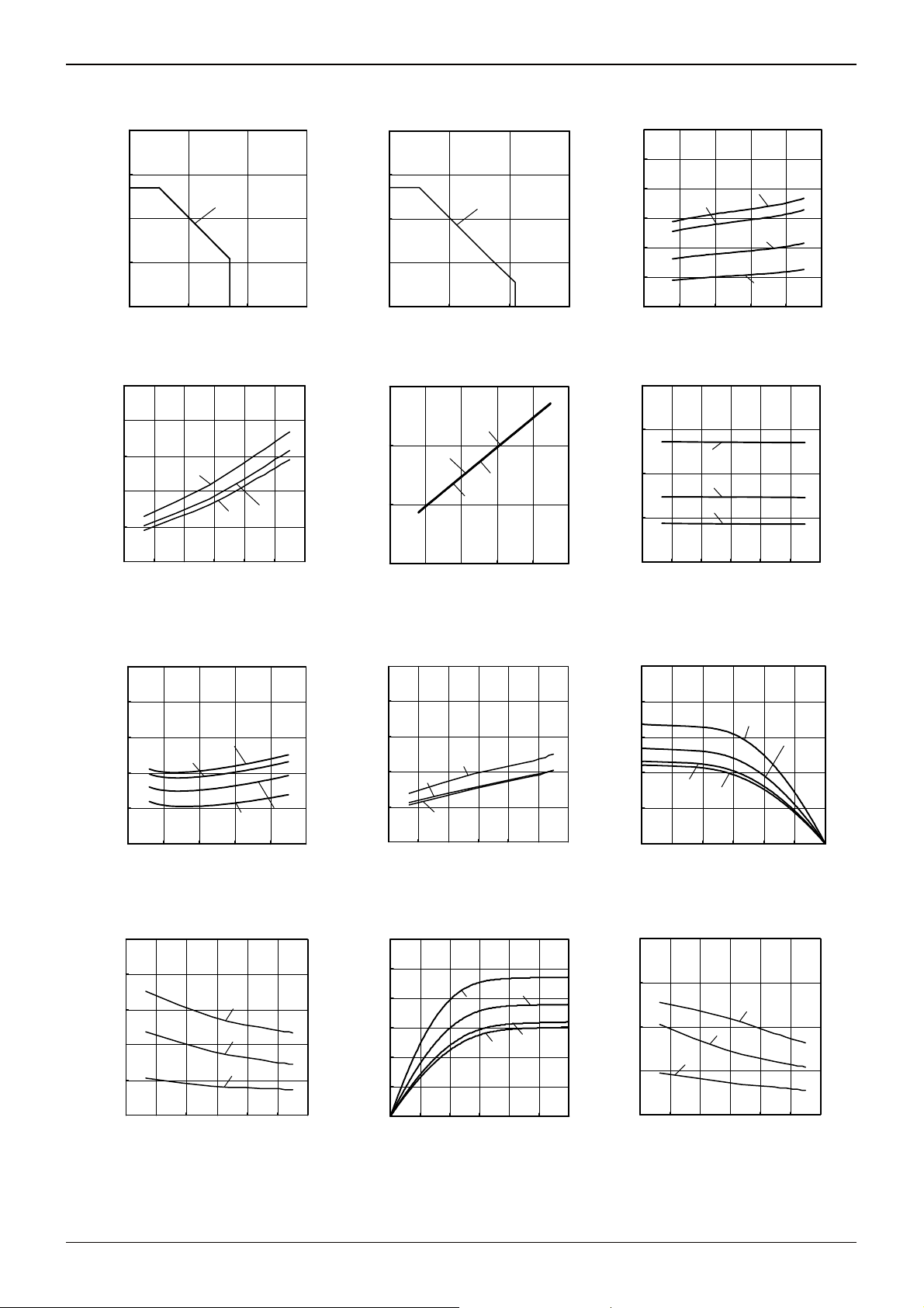
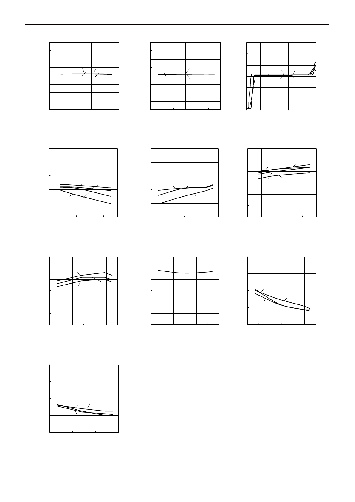
●Example of electrical characteristics
○BU7251 family
800
600
400
BU7251G
200
POWER DISSIPATION [mW] .
0
0 50 100 150
AMBIENT TEMPERATURE [℃]
Fig. 1 Fig. 2 Fig. 3
50
Derating Curve
BU7251 famil
BU7251 famil
800
600
BU7251SG
400
200
POWER DISSIPATION [mW]
0
050100150
AMBIENT TEMPERATURE [℃]
BU7251 famil
Derating Curve
6
BU7251 family
60
50
40
30
20
SUPPLY CURRENT [μA]
10
0
123456
85℃
SUPPLY VOLTAGE [V]
BU7251 family
105℃
25℃
-40℃
Supply Current – Supply Voltage
8
BU7251 famil
40
30
20
SUPPLY CURRENT [μA]
10
5.5V
1.8V
0
-60 -30 0 30 60 90 120
AMBIENT TEMPERATURE [℃]
Fig. 4 Fig. 5 Fig. 6
Supply Current – Ambient Temperature
50
3.0V
BU7251 famil
4
2
OUTPUT VOLTAGE HIGH [V]
0
123456
Output Voltage High – Supply Voltage
50
105℃
85℃
25℃
-40℃
SUPPLY VOLTAGE [V]
(RL=10[kΩ])
BU7251 famil
6
5.5V
4
2
OUTPUT VOLTAGE HIGH [V]
0
-60 -30 0 30 60 90 120
3.0V
1.8V
AMBIENT TEMPERATURE [℃]
Output Voltage High – Ambient Temperature
(RL=10[kΩ])
10
BU7251 famil
40
40
30
20
10
OUTPUT VOLTAGE LOW [mV]
0
123456
Fig. 7 Fig. 8 Fig. 9
Output Voltage Low – Supply Voltage
5
4
105℃
85℃
-40℃
SUPPLY VOLTAGE [V]
(RL=10[kΩ])
25℃
BU7251 famil
3
5.5V
2
1
OUTPUT SOURCE CU RRENT [mA]
0
-60 -30 0 30 60 90 120
AMBIENT TEMPERATURE [℃]
3.0V
1.8V
Fig. 10 Fig. 11 Fig. 12
Output Source Current – Ambient Temperature
(*) The above date is ability value of sample, it is not guaranteed. BU7251G:-40[℃] to+85[℃] BU7251SG:-40[℃] to+105[℃]
(VOUT=VDD-0.4[V])
30
20
10
OUTPUT VOLTAGE LOW [mV]
0
-60 -30 0 30 60 90 120
5.5V
1.8V
3.0V
AMBIENT TEMPERATURE [℃]
Output Voltage Low – Ambient
-40℃
(RL=10[kΩ])
BU7251 famil
25℃
85℃
105℃
Temperature
30
25
20
15
10
5
OUTPUT SINK CURRENT [mA]
0
0.0 0.5 1.0 1.5 2.0 2.5 3.0
OUTPUT VOLTAGE [V]
Output Sink Current – Output Voltage
(VDD=3[V])
8
-40℃
6
4
2
OUTPUT SOURCE CURRENT [mA]
0
85℃
105℃
0.0 0.5 1.0 1.5 2.0 2.5 3.0
OUTPUT VOLTAGE [V]
25℃
Output Source Current – Supply
(VDD=3[V])
Voltage
20
15
10
5
OUTPUT SINK CURRENT [ mA]
0
-60-300306090120
3.0V
1.8V
AMBIENT TEMPERATURE [℃]
BU7251 family
5.5V
Output Sink Current – Ambient Temperature
(VOUT=VSS+0.4[V])
4/18
BU7251G,BU7251SG, BU7231G,BU7231SG,
y
y
y
y
y
BU7252F/FVM,BU7252S F/FVM,BU7232F/FVM,BU7232S F/FVM
Technical Note
○BU7251 family
10.0
7.5
5.0
2.5
0.0
-2.5
-5.0
INPUT OFFSET VOLTAGE [mV]
-7.5
-10.0
123456
Fig. 13 Fig. 14 Fig. 15
Input Offset Voltage – Supply Voltage
(Vicm=VDD, Vout=0.1[V])
160
85℃
25℃
SUPPLY VOLTAGE [V]
105℃
-40℃
BU7251 family
BU7251 famil
10.0
7.5
5.0
2.5
INPUT OFFSET VOLTAGE [mV]
0.0
-2.5
-5.0
-7.5
-10.0
5.5V
-60 -30 0 30 60 90 120
AMBIENT TEMPERATURE [℃]
BU7251 famil
3.0V
1.8V
Input Offset Voltage – Ambient Temperature
(Vicm=VDD, Vout=0.1[V])
160
BU7251 family
15
10
5
0
-5
-10
INPUT OFFSET VOLTAGE [mV]
-15
-1 0 1 2 3 4
INPUT VOLTAGE [V]
85℃
-40℃
105℃
25℃
Input offset voltage – Input Voltage
(VDD=3[V])
120
BU7251 famil
BU7251 family
140
140
120
105℃
100
80
LARGE SIGNAL VOLTAGE GAIN [dB]
60
Fig. 16 Fig. 17 Fig. 18
Large Signal Voltage Gain – Supply Voltage
-40℃
123456
SUPPLY VOLTAGE [V]
85℃
25℃
120
BU7251 family
120
100
80
LARGE SIGNAL VOLTAGE GAIN [dB]
60
-60 -30 0 30 60 90 120
1.8V
3.0V
5.5V
AMBIENT TEMPERATURE [℃]
Large Signal Voltage Gain
– Ambient Temperature
120
BU7251 famil
100
80
60
40
20
COMMON MODE REJECT ION RATIO [dB]
0
123456
85℃
105℃
SUPPLY VOLTAGE [V]
25℃
-40℃
Common Mode rejection Ratio
– Supply Voltage
2.0
(VDD=3[V])
BU7251 family
100
80
60
40
20
COMMON MODE REJECT ION RATIO [dB]
0
-60 -30 0 30 60 90 120
Fig. 19 Fig. 20 Fig. 21
Common Mode Rejection Ratio –
0.8
5.5V
1.8V
AMBIENT TEMPERATURE [
3.0V
Ambient Temperature
(VDD=3[V])
BU7251 famil
]
℃
100
80
60
40
20
POWER SUPPLY REJECT ION RATIO [dB]
0
-60 -30 0 30 60 90 120
AMBIENT TEMPERATURE [
Power Supply Rejection –
Ambient Temperature
1.5
1.0
0.5
PROPAGATION DELAY L-H [μs]
0.0
]
℃
1.8V
5.5V
3.0V
-60 -30 0 30 60 90 120
AMBIENT TEMPERATURE [
]
℃
Propagation Delay L-H –
Ambient Temperature
0.6
0.4
1.8V
5.5V
0.2
PROPAGATION DELAY H-L [μs]
0.0
-60 -30 0 30 60 90 120
Fig. 22
Propagation Delay H-L – Ambient Temperature
(*) The above date is ability value of sample, it is not guaranteed. BU7251G:-40[℃] to+85[℃] BU7251SG:-40[℃] to+105[℃]
3.0V
AMBIENT TEMPERATURE [℃]
5/18
BU7251G,BU7251SG, BU7231G,BU7231SG,
y
y
y
y
y
y
y
BU7252F/FVM,BU7252S F/FVM,BU7232F/FVM,BU7232S F/FVM
Technical Note
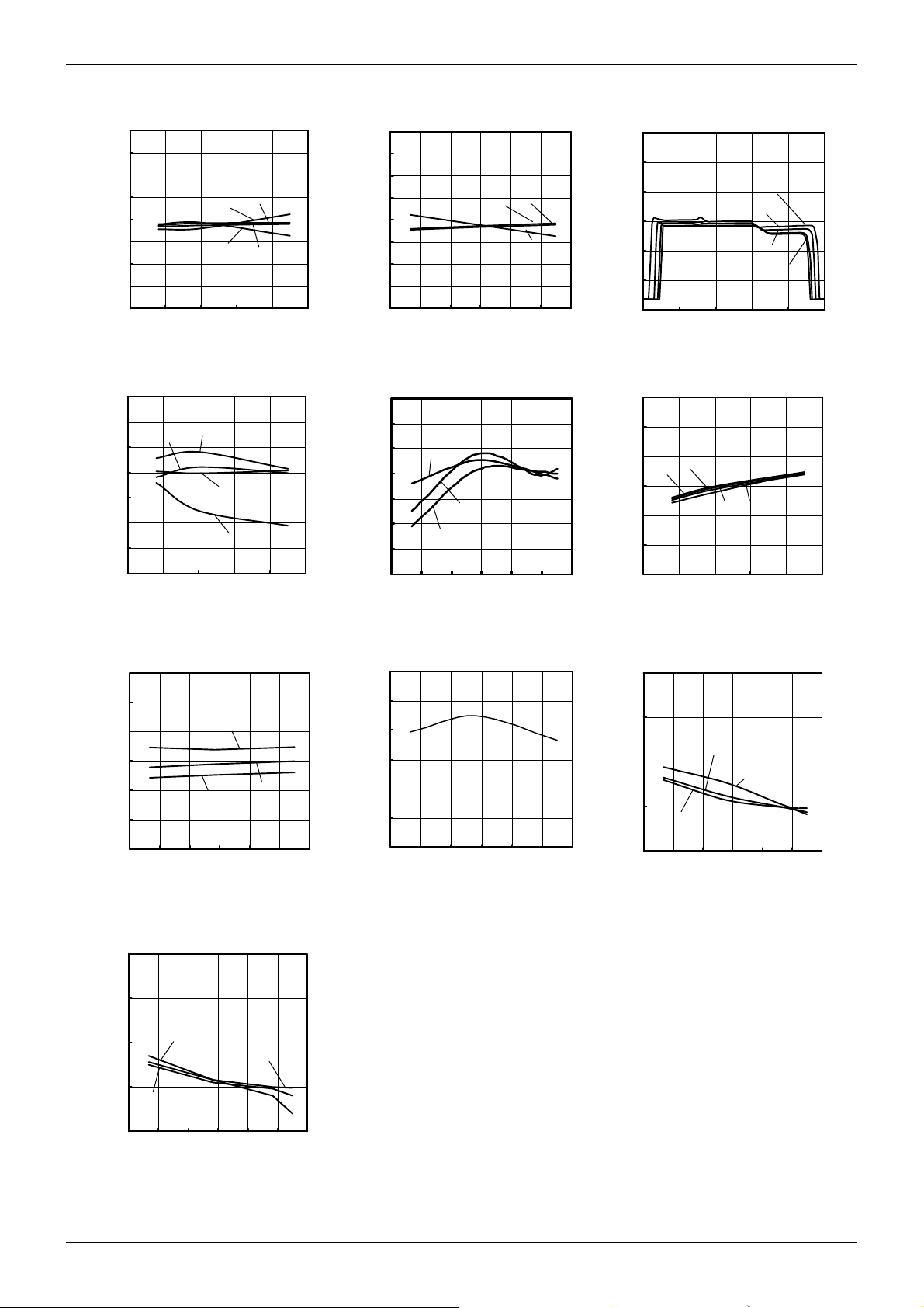
○BU7252 family
1000
800
600
400
POWER DISSIPATION [mV]
200
0
0 50 100 150
AMBIENT TEMPERATURE [℃] .
Fig. 23 Fig. 24 Fig. 25
150
BU7252F
Derating Curve
85
BU7252 famil
BU7252FVM
BU7252 family
1000
800
600
400
PO WER DIS SIPATION [ mV]
200
0
0 50 100 150
AMBIENT TEMPERATURE [℃] .
BU7252SF
Derating Curve
8
BU7252 family
BU7252SFVM
105
BU7252 family
150
100
50
SUPPLY CURRENT [μA]
0
-40℃
123456
SUPPLY VOLTAGE [V]
Supply Current – Supply Voltage
8
100
50
SUPPLY CURRENT [μA]
1.8V
3.0V
0
-60 -30 0 30 60 90 120
AMBIENT T E MPERATURE [
Fig. 26 Fig. 27 Fig. 28
Supply Curreny – Ambient Temperature
50
5.5V
℃
BU7252 famil
]
6
4
2
OUTPUT VOLTAGE HIGH [V]
0
123456
105℃
85℃
25℃
-40℃
SUPPLY VOLTAGE [V]
Output Voltage High – Supply Voltage
(RL=10[kΩ])
50
BU7252 famil
6
4
2
OUTPUT VOLTAGE HIGH [V]
0
-60 -30 0 30 60 90 120
AMBIENT TEMPERATURE [℃]
Output Voltage High – Ambient Temperature
10
40
30
20
10
OUTPUT VOLTAGE LOW [mV]
0
Fig. 29 Fig. 30 Fig. 31
5
4
3
2
1
OU T PUT SOUR CE C URRENT [mA ]
0
-60-30 0 30 60 90120
Output Source Current – Ambient Temperature
-40℃
123456
SUPPLY VOLTAG E [V]
Output Voltage Low – Supply
Voltage
3.0V
1.8V
AMBIENT TEMPERATURE [℃]
Fig. 32 Fig. 33 Fig. 34
(VOUT=VDD-0.4[V])
85℃
25℃
(RL=10[kΩ])
5.5V
105℃
BU7252 famil
40
30
20
10
OUTPUT VOLTAGE LOW [mV]
0
-60 -30 0 30 60 90 120
AMBIENT TEMPERATURE [℃]
5.5V
3.0V
1.8V
Output Voltage Low – Ambient
-40℃
(RL=10[kΩ])
BU7252 famil
85℃
105℃
Temperature
30
25
20
15
10
OUT PU T S INK CURR E NT [mA ]
25℃
5
0
0.0 0.5 1.0 1.5 2.0 2.5 3.0
OUTPUT VOLTAGE [V]
Output Sink Current – Output Voltage
(VDD=3[V])
(*) The above date is ability value of sample, it is not guaranteed. BU7252 F/FVM:-40[℃] to+85[℃] BU7252S F/FVM:-40[℃] to+105[℃]
8
-40℃
6
4
105℃
2
OUTPUT SOURCE CURRENT [mA]
0
0 0.5 1 1.5 2 2.5 3
OUTPUT VOLTAGE [V]
Output Source Current – Output
Voltage
20
15
10
1.8V
5
OUTPUT SINK CURRENT [ mA]
0
-60-300306090120
AMBIENT TEMPERATURE [℃]
Output Sink Current – Ambient Temperature
(VOUT=VSS+0.4[V])
BU7252 famil
105℃
85℃
25℃
BU7252 family
5.5V
3.0V
1.8V
(RL=10[kΩ])
BU7252 family
25℃
85℃
(VDD=3[V])
BU7252 famil
5.5V
3.0V
6/18
BU7251G,BU7251SG, BU7231G,BU7231SG,
y
y
y
y
y
BU7252F/FVM,BU7252S F/FVM,BU7232F/FVM,BU7232S F/FVM
Technical Note
○BU7252 family
10.0
7.5
5.0
2.5
0.0
-2.5
-5.0
INPUT OFFSET VOLTAGE [mV]
-7.5
-10.0
123456
SUPPLY VOLTAGE[V]
Fig. 35 Fig. 36 Fig. 37
Input Offset Voltage – Supply Voltage
(Vicm=VDD,VOUT=0.1[V])
160
140
120
100
80
60
40
LARGE SIGNAL VOLTAGE GAIN [dB]
20
123456
25℃
105℃
SUPPLY VOLTAGE [V]
Fig. 38 Fig. 39 Fig. 40
Large Signal Voltage Gain – Supply
Voltage
120
-40℃
85℃
85℃
-40℃
BU7252 famil
25℃
105℃
BU7252 family
BU7252 family
1.8V
BU7252 family
3.0V
5.5V
10.0
7.5
5.0
2.5
0.0
-2.5
-5.0
INPUT OFFSET VOLTAGE [mV]
-7.5
-10.0
-60 -30 0 30 60 90 120
AMBIENT TEM PE RAT URE [℃]
Input Offset Voltage – Ambient Temperature
(Vicm=VDD,VOUT=0.1[V])
160
140
120
100
80
60
40
LARGE SIGNAL VOLTAGE GAI N [dB]
20
1.8V
3.0V
5.5V
-60-300 306090120
AMBIENT TEMPERATURE [℃]
BU7252 famil
Large Signal Voltage Gain
– Ambient Temperature
120
BU7252 family
15
10
5
0
-5
-10
INPUT OFFSET VOLTAGE [mV]
-15
-1 0 1 2 3 4
INPUT VOLTAGE [V]
BU7252 famil
-40℃
25℃
105℃
85℃
Input Offset Voltage – Input Voltage
(VDD=3[V])
120
100
80
60
40
20
COMMON MODE REJECTION RATIO [dB]
105℃
85℃
25℃
0
123456
SUPPLY VOLTAGE [V]
BU7252 famil
-40℃
Common Mode Rejection Ratio
– Supply Voltage
2.0
(VDD=3[V])
BU7252 famil
100
80
5.5V
60
40
20
COMMON MODE REJECT ION RATIO [dB]
0
-60 -30 0 30 60 90 120
Fig. 41 Fig. 42 Fig. 43
Common Mode Rejection – Ambient
0.8
1.8V
AMBIENT TEM PERATURE [℃]
Temperature
3.0V
(VDD=3[V])
BU7251 family
100
80
60
40
20
POWER SUPPLY REJECTION RATIO [dB]
0
-60 -30 0 30 60 90 120
AMBIENT TEMPERATURE [℃]
Power Supply Rejection Ratio – Ambient
Temperature
1.5
1.0
0.5
PROPAGATION DELAY L-H [μs]
0.0
-60 -30 0 30 60 90 120
1.8V
5.5V
3.0V
AMBIENT TEMPERATURE [℃]
Propagation Delay L-H – Ambient
Temperature
0.6
0.4
1.8V
3.0V
0.2
PROPAGATION DELAY H-L [μs]
Propagation Delay H-L – Ambient Temperature
5.5V
0.0
-60 -30 0 30 60 90 120
AMBIENT TEMPERATURE [℃]
Fig. 44
(*) The above date is ability value of sample, it is not guaranteed. BU7252 F/FVM:-40[℃] to+85[℃] BU7252S F/FVM:-40[℃] to+105[℃]
7/18
5.5V

BU7251G,BU7251SG, BU7231G,BU7231SG,
]
.
y
y
y
y
y
y
y
y
BU7252F/FVM,BU7252S F/FVM,BU7232F/FVM,BU7232S F/FVM
Technical Note
○BU7231 series
800
BU7231 famil
800
BU7231 famil
20
BU7231 family
600
400
BU7231G
200
POWER DISSIPATION [mW] .
0
0 50 100 150
AMBIENT TEM PERATURE [℃]
Fig. 45 Fig. 46 Fig. 47
12
Derating Curve
85
BU7231 famil
600
400
200
POWER DISSIPATION [mW]
0
050100150
AMBIENT TEMPERATURE [℃]
6
BU7231SG
105
Derating Curve
BU7231 famil
16
12
8
SUPPLY CURRENT [μA]
4
0
123456
85℃
SUPPLY VOLTAGE [V]
105℃
25℃
-40℃
Supply Current – Supply Voltage
8
BU7231 famil
10
5.5V
8
6
3.0V
SUPPLY CURRENT [μA]
4
1.8V
2
-60 -30 0 30 60 90 120
AMBIENT TEMPERATURE [℃]
Fig. 48 Fig. 49 Fig. 50
Supply Current – Ambient Temperature
50
40
BU7231 family
30
20
10
OUTPUT VO LT AGE LOW [mV
0
0246 8
SUPPLY VOLTAGE [V]
Fig. 51 Fig. 52 Fig. 53
105℃
85℃
25℃
-40℃
Output Voltage Low – Supply Voltage
(RL=10[kΩ])
5
BU7231 family
4
3
2
1
OUTP UT SOURCE CURRENT [mA]
0
-60 -30 0 30 60 90 120
AMBIENT TEMPERATURE [℃]
5.5V
3.0V
1.8V
Fig. 54 Fig. 55 Fig. 56
Output Source Current – Ambient Temperature
(VOUT=VDD-0.4[V])
4
2
OUTPUT VOLTAGE HIGH [V]
0
123456
Output Voltage – Supply Voltage
50
40
30
20
1.8V
10
OUTPUT VOLTAGE LOW [mV]
3.0V
0
-60 -30 0 30 60 90 120
AMBIENT TEMPERATURE [℃]
Output Voltage Low – Ambient Temperature
30
25
20
15
10
5
OUTPUT SINK CURRENT [mA]
0
0.0 0.5 1.0 1.5 2.0 2.5 3.0
Output Sink Current – Output Voltage
105℃
85℃
25℃
-40℃
SUPPLY VOLTAGE [V]
(RL=10[kΩ])
5.5V
(RL=10[kΩ])
-40℃
105℃
OUTPUT VOLTAGE [V]
(VDD=3[V])
BU7231 famil
BU7231 family
25℃
85℃
6
5.5V
4
2
OUTPUT VOLTAGE HIGH [V]
0
-60 -30 0 30 60 90 120
3.0V
1.8V
AMBIENT TEMPERATURE [℃]
Output Voltage High – Ambient Temperature
(RL=10[kΩ])
10
8
6
4
2
OUTPUT SOURCE CURRENT [mA]
0
85℃
105℃
0 0.5 1 1.5 2 2.5 3
OUTPUT VOLTAGE [V]
BU7231 famil
-40℃
25℃
Output Source Current – Output Voltage
(VDD=3[V])
20
15
10
5
OUTPUT SINK CURRENT [mA]
0
-60 -30 0 30 60 90 120
3.0V
1.8V
AMBIENT TEMPERATURE [℃]
BU7231 famil
5.5V
Output Sink Current – Ambient Temperature
(VOUT=VSS+0.4[V])
(*) The above date is ability value of sample, it is not guaranteed. BU7231G:-40[℃] to+85[℃] BU7231SG:-40[℃] to+105[℃]
8/18

BU7251G,BU7251SG, BU7231G,BU7231SG,
y
y
y
y
y
y
y
BU7252F/FVM,BU7252S F/FVM,BU7232F/FVM,BU7232S F/FVM
Technical Note
○BU7231 series
25℃
3.0V
BU7231 famil
85℃
BU7231 famil
85℃
BU7231 famil
(VDD=3[V])
10.0
7.5
5.0
2.5
0.0
-2.5
-5.0
INPUT OFFSET VOLTAGE [mV]
-7.5
-10.0
-60 -30 0 30 60 90 120
3.0V
5.5V
AMBIENT TEM PERATURE [℃]
BU7231 famil
1.8V
Input Offset Voltage – Ambient Temperature
(Vicm=VDD, Vout=0.1[V])
160
140
120
100
80
LARGE SIGNAL VOLTAGE GAIN [dB]
60
-60 -30 0 30 60 90 120
3.0V
AMBIENT TEM PERATURE [℃]
BU7231 famil
1.8V
5.5V
Large Signal Voltage Gain
– Ambient Temperature
120
100
80
60
40
20
POWER SUPPLY REJECTION RATIO [dB]
0
-60 -30 0 30 60 90 120
AMBIENT TEMPERATURE [℃]
BU7231 family
Power Supply Rejection Ratio
– Ambient Temperature
85℃
BU7231 famil
105℃
25℃
15
10
5
0
-5
-10
INPUT OFFSET VOLTAGE [mV]
-15
-101234
-40℃
INPUT VOLTAGE [V]
Input Offset Voltage – Input Voltage
(VDD=3[V])
120
100
80
60
40
20
COMMON MODE REJECT ION RATIO [dB]
0
123456
85℃ 105℃
25℃
SUPPLY VOLTAGE [V]
BU7231 family
-40℃
Common Mode Rejection Ratio
– Supply Voltage
5
4
3
2
1
PROPAGATION DELAY L-H [μs]
0
1.8V
-60 -30 0 30 60 90 120
AMBIENT TEM PERATURE [℃]
5.5V
(VDD=3[V])
BU7231 family
3.0V
Propagation Delay L-H
– Ambient Temperature
10.0
7.5
5.0
2.5
0.0
-2.5
-5.0
INPUT OFFS ET VOLTAGE [ mV ]
-7.5
-10.0
123456
Fig. 57 Fig. 58 Fig. 59
Input Offset Voltage – Supply Voltage
(Vicm=VDD, Vout=0.1[V])
160
-40℃
25℃
105℃
SUPPLY VOLTAGE [V]
140
120
100
80
LARGE SIGNAL VOLTAGE GAIN [dB]
60
123456
Fig. 60 Fig. 61 Fig. 62
Large Signal Voltage Gain – Supply Voltage
105℃
-40℃
SUPPLY VOLTAGE [V]
120
100
80
60
40
20
COMMON MODE REJECTION RA TIO [dB]
0
-60 -30 0 30 60 90 120
Fig. 63 Fig. 64 Fig. 65
Common Mode Rejection Ratio
– Ambient Temperature
5.5V
1.8V
AMBIENT TEMPERATURE [℃]
1.5
BU7231 famil
1.2
0.9
0.6
0.3
PROPAGATION DELAY H-L [μs]
0.0
Propagation Delay H-L– Ambient Temperature
(*) The above date is ability value of sample, it is not guaranteed. BU7231G:-40[℃] to+85[℃] BU7231SG:-40[℃] to+105[℃]
1.8V
-60 -30 0 30 60 90 120
AMBIENT TEM PERATURE [℃]
Fig. 66
5.5V
3.0V
9/18

BU7251G,BU7251SG, BU7231G,BU7231SG,
y
y
]
y
y
y
BU7252F/FVM,BU7252S F/FVM,BU7232F/FVM,BU7232S F/FVM
Technical Note
○BU7232 family
1000
800
BU7232 family
1000
800
BU7232 family
50
40
BU7232 family
600
400
POWER DISSIP A TION [mV]
200
0
0 50 100 150
Fig. 67 Fig. 68 Fig. 69
50
BU7232F
BU7232FVM
85
AMBIENT TEMPERATURE [℃] .
Derating Curve
BU7232 famil
600
400
POWER DISSIP A TION [mV]
200
0
0 50 100 150
AMBIENT TEMPERATURE [℃] .
BU7232SF
Derating Curve
8
BU7232SFVM
105
BU7232 famil
30
20
-40℃
SUPPLY CURRE NT [µA]
10
0
123456
105℃
85℃
25℃
SUPPLY VOLTAGE [V]
Supply Current – Supply Voltage
8
BU7232 famil
40
30
20
SUPPLY CURRENT [μA]
10
1.8V
5.5V
3.0V
0
-60-300 306090120
AMBIENT TEMPERATURE [℃]
Fig. 70 Fig. 71 Fig. 72
Supply Current – Ambient emperature
50
40
BU7232 family
30
20
10
OUTPUT VOLTAGE LOW [mV]
0
1234567
Fig. 73 Fig. 74 Fig. 75
Output Voltage Low – Supply Voltage
5
85℃
-40℃
SUPPLY VOLTAGE [V]
(RL=10[kΩ])
105℃
25℃
BU7232 famil
4
5.5V
3
2
1
OUTPUT SOURCE CURRENT [mA]
0
-60 -30 0 30 60 90 120
3.0V
1.8V
AMBIENT TE MPERATURE [℃]
Fig. 76 Fig. 77 Fig. 78
Output Source Current – Ambient Temperature
(VOUT=VDD-0.4[V])
6
4
2
OUTPUT VOLTAGE HIGH [V]
0
1234567
105℃
85℃
25℃
-40℃
SUPPLY VOLTAGE [V]
Output Voltage High – Supply Voltage
(RL=10[kΩ])
40
30
20
10
OUTPUT VOLT AGE LOW [mV
0
-60-300 306090120
3.0V
1.8V
AMBIENT TEMPERATURE [℃]
BU7232 family
5.5V
Output Voltage Low – Ambient temperature
(RL=10[kΩ])
85℃
BU7232 famil
105℃
30
-40℃
25℃
20
10
OUTPUT SINK CURRENT [mA]
0
0.0 0.5 1.0 1.5 2.0 2.5 3.0
OUTPUT VOLTAGE [V]
Output Sink Current – Output Voltage
(VDD=3[V])
6
4
2
OUTPUT VOLTAGE HIGH [V]
0
-60 -30 0 30 60 90 120
Output Voltage – Ambient Temperature
10
8
-40℃
6
4
2
OUTPUT SO URCE CURRENT [mA]
0
00.511.522.53
Output Source Current – Output Voltage
20
15
10
5
OUTPUT SI NK CURRENT [mA]
0
-60 -30 0 30 60 90 120
Output Sink Current – Ambient Temperature
(*) The above date is ability value of sample, it is not guaranteed. BU7232 F/FVM:-40[℃] to+85[℃] BU7232S F/FVM:-40[℃] to+105[℃]
5.5V
3.0V
1.5V
AMBIENT TEMPERATURE [
(RL=10[kΩ])
25℃
85℃
105℃
OUTPUT VOLTAGE [V]
BU7232 family
(VDD=3[V])
BU7232 family
5.5V
3.0V
1.8V
AMBIENT TEMPERATURE [℃]
(VOUT=VSS+0.4[V])
]
℃
10/18

BU7251G,BU7251SG, BU7231G,BU7231SG,
y
y
y
y
y
y
BU7252F/FVM,BU7252S F/FVM,BU7232F/FVM,BU7232S F/FVM
Technical Note
○BU7232 family
10.0
7.5
5.0
2.5
0.0
-2.5
-5.0
INPUT OFFSET VOLTAGE [mV]
-7.5
-10.0
Input Offset Voltage – Ambient Temperature
160
85℃
123456
AMBIENT TEMPERATURE [
-40℃
Fig. 79 Fig. 80 Fig. 81
(Vicm=VDD, VOUT=0.1[V])
105℃
BU7232 famil
25℃
℃
BU7232 famil
BU7232 family
3.0V
BU7232 famil
5.5V
]
℃
15
10
-40℃
5
0
-5
-10
INPUT OFFSET VOLTAGE [mV]
-15
-101234
105℃
85℃
25℃
INPUT VOLTAGE [V]
10.0
7.5
5.0
2.5
0.0
-2.5
-5.0
INPUT OFFSET VOLTAGE [mV]
-7.5
-10.0
]
-60 -30 0 30 60 90 120
1.8V
AMBIENT TEMPERATURE [
Input Offset Voltage – Ambient Temperature
(Vicm=VDD, VOUT=0.1[V])
160
BU7232 famil
Input Offset Voltage – Input Voltage
(VDD=3[V])
120
BU7232 family
140
140
120
100
80
LARGE SIGNAL VOLTAGE GAIN [dB]
60
123456
Fig. 82 Fig. 83 Fig. 84
Large Signal Voltage Gain – Supply Voltage
25℃
105℃
-40℃
SUPPLY VOLTAGE [V]
85℃
5.5V
3.0V
BU7232 family
(VDD=3[V])
BU7232 famil
120
100
80
60
40
20
COMMON MODE REJECTION RA TIO [dB]
0
-60 -30 0 30 60 90 120
Fig. 85 Fig. 86 Fig. 87
Common Mode Rejection Ratio –
Ambient Temperature
1.5
1.2
1.8V
AMBIENT TEMPERATURE [℃]
120
100
80
LARGE SIGNAL VOLTAGE GAIN [dB]
60
-60 -30 0 30 60 90 120
1.8V
5.5V
3.0V
AMBIENT TEMPERATURE [
Large Signal Voltage Gain
– Ambient Temperature
120
100
80
60
40
20
POWER SUPPLY REJECTION RATIO [dB]
0
-60 -30 0 30 60 90 120
AMBIENT TEMPERATURE [℃]
Power Supply Rejection Ratio
– Ambient Temperature
]
℃
BU7232 famil
100
80
60
40
20
COMMON MODE REJECTI ON RATIO [dB]
0
123456
105℃
-40℃
25℃
SUPPLY VOLTAGE [V]
Common Mode Rejection Ratio
– Supply Voltage
5
4
3
2
1
PROPAGATION DELAY L-H [μs]
0
5.5V
-60 -30 0 30 60 90 120
AMBIENT TEMPERATURE [℃]
(VDD=3[V])
BU7232 family
3.0V
1.8V
Propagation Delay L-H – Ambient
temperature
0.9
0.6
0.3
PROPAGATION DELAY H-L [us]
0.0
Propagation Delay H-L – Ambient Temperature
(*) The above date is ability value of sample, it is not guaranteed. BU7232 F/FVM:-40[℃] to+85[℃] BU7232S F/FVM:-40[℃] to+105[℃]
5.5V
1.8V
3.0V
-60 -30 0 30 60 90 120
AMBIENT TEMPERATURE [℃]
Fig. 88
11/18

BU7251G,BU7251SG, BU7231G,BU7231SG,
KEKRK
F
m
BU7252F/FVM,BU7252S F/FVM,BU7232F/FVM,BU7232S F/FVM
Technical Note
●Schematic diagram
Fig. 89 Simplified schematic
●Test circuit1 NULL method
VDD,VSS,EK,Vicm, Unit : [V]
Parameter VF S1 S2 S3
VDD VSS EK Vicm
Input offset voltage VF1 ON ON OFF 3 0 -0.1 0.3 1
Large signal voltage gain
Common-mode rejection ratio
(Input common-mode voltage range)
Power supply rejection ratio
VF2
VF3 -2.7
VF4
VF5 3
VF6
VF7 5.5
ON ON ON 3 0
ON ON OFF 3 0 -0.1
ON ON OFF
1.8
-0.3
0.3 2
0 -0.1 0.3 4
-Calculation-
1. Input offset Voltage (Vio)
Vio =
|VF1|
1+Rf/Rs
[V]
2. Large signal voltage gain (Av)
3. Common-mode rejection ratio (CMRR)
4. Power supply rejection ratio (PSRR)
0.47[μF]
RS=50[Ω]
Vic
RS=50[Ω]
S1
0.1[uF]
Ri=1[MΩ]
Ri=1[MΩ]
0.1[uF]
VDD
DUT
VSS
50[kΩ]
S2
Rf
50[kΩ]
S3
RL
500[kΩ]0.01[μF]
500[kΩ]
R
NULL
+15[V]
-15[V]
V
Fig. 90 Test Circuit 1 (one channel only)
0
Calculation
3
12/18

BU7251G,BU7251SG, BU7231G,BU7231SG,
6SW7SW4SW3CLSW8RL
o
BU7252F/FVM,BU7252S F/FVM,BU7232F/FVM,BU7232S F/FVM
Technical Note
●Test circuit2 switch condition
Unit : [V]
SW No.
SW
1
SW
2
SW
3
SW
4
SW
5
SW
6
SW
7
supply current OFF ON ON OFF OFF OFF OFF OFF
maximum output voltage RL=10 [kΩ] OFF ON ON ON OFF OFF ON OFF
output current OFF OFF OFF OFF OFF ON OFF OFF
response time ON OFF ON OFF ON OFF OFF ON
VDD=3[V]
-
SW1 SW2
+
SW5SW
VIN- VIN+
GND
V
Fig. 91 Test circuit2 (one channel only)
1.6[V]
V
IN
[V]
Input Wav e Input Wav e
入力波形
Vref=1.5[V]
1.4[V]
3[V]
100mV over drive
V
OUT
[V]
Out put Wave Output Wave
出力波形
Vref=1.5[V]
1.6[V]
1.4[V]
3[V]
V
IN
[V]
V
OUT
[V]
入力波形
100mV over drive
t
出力波形
1.5[V]
1.5[V]
0[V]
t
TPHL
0[V]
t
TPLH
Fig. 92 Slew rate input output wave
SW
8
13/18

BU7251G,BU7251SG, BU7231G,BU7231SG,
BU7252F/FVM,BU7252S F/FVM,BU7232F/FVM,BU7232S F/FVM
●Description of electrical characteristics
Described here are the terms of electric characteristics used in this technical note. Items and symbols used are also shown.
Note that item name and symbol and their meaning may differ from those on another manufacture’s document or general
document.
1. Absolute maximum ratings
Absolute maximum rating item indicates the condition which must not be exceeded. Application of voltage in excess of absolute
Maximum rating or use out of absolute maximum rated temperature environment may cause deterioration of characteristics.
1.1 Power supply voltage(VDD/VSS)
Indicates the maximum voltage that can be applied between the positive power supply terminal and negative power supply
terminal without deterioration or destruction of characteristics of internal circuit.
1.2 Differential input voltage (Vid)
Indicates the maximum voltage that can be applied between non-inverting terminal and inverting terminal without
deterioration and destruction of characteristics of IC.
1.3 Input common-mode voltage range (Vicm)
Indicates the maximum voltage that can be applied to non-inverting terminal and inverting terminal without deterioration or
destruction of characteristics. Input common-mode voltage range of the maximum ratings not assure normal operation of IC.
When normal operation of IC is desired, the input common-mode voltage of characteristics item must be followed.
1.4 Power dissipation (Pd)
Indicates the power that can be consumed by specified mounte d board at the ambient temperature 25℃(normal temperature).
As for package product, Pd is determined by the temperature that can be permitted by IC chip in the package(maximum
junction temperature) and thermal resistance of the package
2. Electrical characteristics item
2.1 Input offset voltage (Vio)
Indicates the voltage difference between non-inverting terminal and inverting terminal.
It can be translated into the input voltage difference required for setting the output voltage at 0 [V]
2.2 Input offset current (Iio)
Indicates the difference of input bias current between non-inverting terminal and inverting terminal.
2.3 Input bias current (Ib)
Indicates the current that flows into or out of the input terminal. It is defined by the average of input bias current at
non-inverting terminal and input bias current at inverting terminal.
2.4 Input common-mode voltage range (Vicm)
Indicates the input voltage range where IC operates normally.
2.5 Large signal voltage gain (AV)
Indicates the amplifying rate (gain) of output voltage against the voltage difference between non-inverting terminal and
inverting terminal. It is normally the amplifying rate (gain) with reference to DC voltage.
Av = (Output voltage fluctuation) / (Input offset fluctuation)
2.6 Circuit current (ICC)
Indicates the IC current that flows under specified conditions and no-load steady status.
2.7 Output sink current (OL)
Indicates the maximum current that can be output under specified output condition (such as output vol tage and load condi tion).
2.8 Output saturation voltage, Low level output voltage (VOL)
Indicates the voltage range that can be output under specified load conditions.
2.9 Output leakage current, High level output current(I leak)
Indicates the current that flows into IC under specified input and output conditions.
2.10 Response Time (Tre)
The interval between the application of an input and output condition.
2.11 Common-mode rejection ratio (CMRR)
Indicates the ratio of fluctuation of input offset voltage when in-phase input voltage is changed. It is normally the fluctuation of DC.
CMRR =(Change of Input common-mode voltage)/(Input offset fluctuation)
2.12 Power supply rejection ratio (PSRR)
Indicates the ratio of fluctuation of input offset voltage when supply voltage is changed. It is normally the fluctuation of DC.
PSRR=(Change of power supply voltage)/(Input offset fluctuation)
Technical Note
14/18

BU7251G,BU7251SG, BU7231G,BU7231SG,
A
[
.
.
.
.
A
[
BU7252F/FVM,BU7252S F/FVM,BU7232F/FVM,BU7232S F/FVM
Technical Note
●Derating curve
Power dissipation (total loss) indicates the pow er that can be consumed by IC at Ta=25℃(normal temperature).IC is heated
when it consumed power , and the tempe rature of IC ship be comes higher than ambient temperature. The temperature that
can be accepted by IC chip depends on circuit configuration, manufacturing process, and co nsumable pow er is limited. Power
dissipation is determined by the temperature all owed in IC chip (maximum junction tempe rature) and thermal resist ance o f
package (heat dissipation capa bility ). The maximum jun ction te mperature is typically equal to the maximum val ue in the
storage package (heat dissipation capability ). The maximum ju nction temperature is typically equal to the maximum value in
the storage temperature range. Heat generated by consumed pow er of IC radiates from the mol d resin or lead frame of the
package. The parameter w hich indicates thi s heat dissip ation cap ability (hardness of heat relea se) is called thermal
resistance, represented by the symbol θj-a[℃/W]. The temperature of IC insid e the p a ckage can be estima ted by this thermal
resistance. Fig.93 (a) shows the model of thermal resistance of the p ackage. Thermal resista nce θja, ambient temperature Ta,
junction temperature Tj, and power dissipation Pd can be cal culated by the equation below :
θja = (Tj-Ta) / Pd [℃/W] ・・・・・ (Ⅰ)
Derating curve in Fig.93 (b) indicates power that can be consu med by IC with reference to a mbient tempera ture. Pow er that
can be consumed by IC begins to attenuate at certain ambien t tempera ture. This gradient is determined by thermal
resistance θja. Thermal resistance θja depends on chip size , pow er consumption, p ackage, ambient temperature , package
condition, wind velocity, etc even when the same of package is used. Thermal reduction curve indicates a reference value
measured at a specified condition. Fig94(c)-(f) show a derating curve for an ex ample of BU7251family, BU7252 family, BU7231
family , BU7232 family.
θja = ( Tj ーTa ) / Pd [℃/W]
Power dissipation Pd:[W]
LSI
P2
の消費電力
Pd(max)
[W]
θja2 < θja1
mbient temperature Ta
Chip surface temperature Tj [℃]
Pow er di ssipa tio n P [ W]
(a) Thermal resistance
800
600
400
200
POWER DISSIPATION [mW]
0
050100150
AMBIENT TEMPERATURE [
(c) BU7251G BU7231G
800
600
400
200
POWER DISSIPATION [mW]
0
0 50 100 150
AMBIENT TEMPERATURE [
(e) BU7251SG BU7231SG (f) BU7252S F/FVM BU72432S F/FVM
]
℃
P1
θja1
0507510012515025
mbient temperature:Ta
周囲温度
Ta[℃]
℃
(b) Derating curve
Fig. 93. Thermal resistance and power dissipation
1000
800
BU7251G(*8)
540[mw]
85
540[mw]
BU7231G(*8)
]
℃
BU7251SG(*8)
BU7231SG(*8)
105
]
℃
600
400
200
POWER DISSIPATION [mW]
0
0 50 100 150
AMBIENT TEMPERATURE [℃]
(d) BU7252F/FVM BU7232F/FVM
1000
800
600
400
200
POWER DISSIPATION [mW]
0
0 50 100 150
620[mw]
480[mw]
AMBIENT TEMPERATURE [℃]
]
BU7251/BU7231
620[mw]
480[mw]
85
BU7252SF(*9)
BU7232SF(*9)
BU7252SFVM(*10)
BU7232SFVM(*10)
θja2
Tj(max)
BU7252F(*9)
BU7232F(*9)
BU7252FVM(*10)
BU7232FVM(*10)
105
Tj(max)
(*8) (*9) (*10) Unit
5.4 6.2 4.8 [mW/℃]
When using the unit above Ta=25[℃], subtract the value above per degree[℃]. Permissible dissipation is the value
when FR4 glass epoxy board 70[mm]×70[mm]×1.6[mm] (cooper foil area below 3[%]) is mounted.
Fig. 94.
Derating curve
15/18

BU7251G,BU7251SG, BU7231G,BU7231SG,
BU7252F/FVM,BU7252S F/FVM,BU7232F/FVM,BU7232S F/FVM
●Notes for use
1) Absolute maximum ratings
Absolute maximum ratings are the values which indicate the limits, within which the given voltage range can be safel y
charged to the terminal.However, it does not guarantee the circuit operation.
2) Applied voltage to the input terminal
For normal circuit operation of voltage comparator, please input voltage for its input terminal within input common mode
voltage VDD+0.3[V].Then, regardless of power supply voltage,VSS-0.3[V] can be applied to inputterminals without
deterioration or destruction of its characteristics.
3) Operating power supply (split power supply/single power supply)
The voltage comparator operates if a given level of voltage is applied between VDD and VSS.
Therefore, the operational amplifier can be operated under single power supply or split power supply.
4) Power dissipation (pd)
If the IC is used under excessive power dissipation. An increase in the chip temperature will cause deterioration of the
radical characteristics of IC. For example, reduction of current capability.
Take consideration of the effective power dissipation and thermal design with a sufficient margin. Pd is reference to the
provided power dissipation curve.
5) Short circuits between pins and incorrect mounting
Short circuits between pins and incorrect mounting when mounting the IC on a printed circuits board, take notice of the
direction and positioning of the IC.
If IC is mounted erroneously, It may be damaged. Also, when a foreign object is inserted between output, between output
and VDD terminal or VSS terminal which causes short circuit, the IC may be damaged.
6) Using under strong electromagnetic field
Be careful when using the IC under strong electromagnetic field because it may malfunction.
7) Usage of IC
When stress is applied to the IC through warp of the printed circuit board,
The characteristics may fluctuate due to the piezo effect. Be careful of the warp of the printed circuit board.
8) Testing IC on the set board
When testing IC on the set board, in cases where the capacitor is connected to the low impedance,make sure to
discharge per fabrication because there is a possibility that IC may be damaged by stress.
When removing IC from the set board, it is essential to cut supply voltage.
As a countermeasure against the static electricity, observe proper grounding during fabrication process and take due
care when carrying and storage it.
9) The IC destruction caused by capacitive load
The transistors in circuits may be damaged when VDD terminal and VSS terminal is shorted with the charged output
terminal capacitor.
When IC is used as a operational amplifier or as an application circuit,where oscillation is not activated by an output
capacitor,the output capacitor must be kept below 0.1[μF] in order to prevent the damage mentioned above.
10) Decupling capacitor
Insert the deculing capacitance between VDD and VSS, for stable operation of operational amplifier.
11) Latch up
Be careful of input vltage that exceed the VDD and VSS. When CMOS device have sometimes occur latch up operation.
And protect the IC from abnormaly noise
Technical Note
16/18

BU7251G,BU7251SG, BU7231G,BU7231SG,
BU7252F/FVM,BU7252S F/FVM,BU7232F/FVM,BU7232S F/FVM
●Ordering part number
B U 7 2 5 2 F V M - T R
Technical Note
Part No. Part No.
Package
7231 , 7231S
7251 , 7251S
7252 , 7252S
7232 , 7232S
SOP8
5.0±0.2
(MAX 5.35 include BURR)
7
6
+
6
°
4
°
−4°
<Tape and Reel information>
0.17
0.3MIN
+0.1
-
0.05
(Unit : mm)
0.9±0.15
4.4±0.2
6.2±0.3
438251
0.595
1.5±0.1
0.11
1.27
S
0.42±0.1
SSOP5
2.8±0.2
2.9±0.2
5
4
+0.2
−0.1
1.6
12
3
4
0.13
°
+
6
°
°
−4
0.2Min.
+0.05
−0.03
<Tape and Reel information>
1.25Max.
1.1±0.05
0.05±0.05
0.95
+0.05
0.42
−0.04
0.1
(Unit : mm)
G: SSOP5
F: SOP8
FVM: MSOP8
Embossed carrier tapeTape
Quantity
Direction
of feed
Quantity
Direction
of feed
2500pcs
E2
()
Embossed carrier tapeTape
3000pcs
TR
()
Packaging and forming specification
E2: Embossed tape and reel
(SOP8)
TR: Embossed tape and reel
(SSOP5/MSOP8)
The direction is the 1pin of product is at the upper left when you hold
reel on the left hand and you pull out the tape on the right hand
Reel
The direction is the 1pin of product is at the upper right when you hold
reel on the left hand and you pull out the tape on the right hand
Reel
1pin
Order quantity needs to be multiple of the minimum quantity.
∗
1pin
Order quantity needs to be multiple of the minimum quantity.
∗
Direction of feed
Direction of feed
17/18

BU7251G,BU7251SG, BU7231G,BU7231SG,
BU7252F/FVM,BU7252S F/FVM,BU7232F/FVM,BU7232S F/FVM
MSOP8
<Tape and Reel information>
Quantity
Direction
of feed
(MAX 3.25 include BURR)
2.8±0.1
4.0±0.2
0.475
0.9MAX
0.75±0.05
0.08±0.05
2.9±0.1
8
1
2
0.65
6
57
4
3
1PIN MARK
+0.05
0.22
–0.04
0.08 S
+
6°
4°
−4°
0.6±0.2
0.29±0.15
+0.05
0.145
–0.03
S
(Unit : mm)
Technical Note
Embossed carrier tapeTape
3000pcs
TR
The direction is the 1pin of product is at the upper right when you hold
()
reel on the left hand and you pull out the tape on the right hand
1pin
Direction of feed
Reel
Order quantity needs to be multiple of the minimum quantity.
∗
18/18

Notes
No copying or reproduction of this document, in part or in whole, is permitted without the
consent of ROHM Co.,Ltd.
The content specied herein is subject to change for improvement without notice.
The content specied herein is for the purpose of introducing ROHM's products (hereinafter
"Products"). If you wish to use any such Product, please be sure to refer to the specications,
which can be obtained from ROHM upon request.
Examples of application circuits, circuit constants and any other information contained herein
illustrate the standard usage and operations of the Products. The peripheral conditions must
be taken into account when designing circuits for mass production.
Great care was taken in ensuring the accuracy of the information specied in this document.
However, should you incur any damage arising from any inaccuracy or misprint of such
information, ROHM shall bear no responsibility for such damage.
The technical information specied herein is intended only to show the typical functions of and
examples of application circuits for the Products. ROHM does not grant you, explicitly or
implicitly, any license to use or exercise intellectual property or other rights held by ROHM and
other par ties. ROHM shall bear no responsibility whatsoever for any dispute arising from the
use of such technical information.
Notice
The Products specied in this document are intended to be used with general-use electronic
equipment or devices (such as audio visual equipment, ofce-automation equipment, communication devices, electronic appliances and amusement devices).
The Products specied in this document are not designed to be radiation tolerant.
While ROHM always makes efforts to enhance the quality and reliability of its Products, a
Product may fail or malfunction for a variety of reasons.
Please be sure to implement in your equipment using the Products safety measures to guard
against the possibility of physical injury, re or any other damage caused in the event of the
failure of any Product, such as derating, redundancy, re control and fail-safe designs. ROHM
shall bear no responsibility whatsoever for your use of any Product outside of the prescribed
scope or not in accordance with the instruction manual.
The Products are not designed or manufactured to be used with any equipment, device or
system which requires an extremely high level of reliability the failure or malfunction of which
may result in a direct threat to human life or create a risk of human injury (such as a medical
instrument, transpor tation equipment, aerospace machinery, nuclear-reactor controller,
fuel-controller or other safety device). ROHM shall bear no responsibility in any way for use of
any of the Products for the above special purposes. If a Product is intended to be used for any
such special purpose, please contact a ROHM sales representative before purchasing.
If you intend to export or ship overseas any Product or technology specied herein that may
be controlled under the Foreign Exchange and the Foreign Trade Law, you will be required to
obtain a license or permit under the Law.
www.rohm.com
© 2009 ROHM Co., Ltd. All rights reserved.
Thank you for your accessing to ROHM product informations.
More detail product informations and catalogs are available, please contact us.
ROHM Customer Support System
http://www.rohm.com/contact/
R0039
A
 Loading...