


Compact Headphone Amplifiers
Headphone Amplifier
Designed for 0.93V Low Voltage Operation
BU7150NUV
●Description
BU7150NUV is Audio Amplifier designed for Single-cell battery operated audio products (VDD = 0.93 ~ 3.5V, at Ta=0~85°C).
BU7150NUV can be selected in single-ended mode for stereo headphone and BTL mode for mono speaker operations. For
BU7150NUV at VDD = 1.5V, THD+N = 1%, the output power is 14mW at RL = 16Ω in single-ended mode and the output
power is 85mW at RL = 8Ω in BTL mode.
●Features
1) Wide battery operation Voltage
2) BU7150NUV can be selected in single-ended mode for stereo headphone and BTL mode for mono speaker operation
3) Unity-gain stability
4) Click and pop-noise reduction circuit built-in
5) Shutdown mode(Low power mode)
6) High speed turn-on mute mode
7) Thermal shutdown protection circuit
8) Power-on reset circuit not sensed during start-up slew rate of supply voltage
9) Small package (VSON010V3030)
●Applications
Noise-canceling headphone, IC recorder, Mobile phone, PDA, Electronic toys etc..
●Absolute Maximum Ratings (Ta=25℃)
Parameter Symbol Ratings Unit
Supply Voltage VDD 4.5 V
(0.93V~3.5V, Ta=0~85°C) (1.03V~3.5V, Ta= -40~85°C)
No.11102ECT01
Input Voltage VIN VSS-0.3~VDD+0.3 V
Input Current IIN -10~10 mA
Power Dissipation PD 560 * mW
Storage Temperature Range TSTG -55~+150 °C
*For operating over 25°C, de-rate the value at 5.6mW/°C.
This value is for IC mounted on 74.2 mm x 74.2mm x 1.6mm glass-epoxy PCB of single-layer.
●Operating conditions
Parameter Symbol
Operation Temperature Range TOPR -40 - 85 °C
Supply Voltage (Note 1,2) VDD 0.93 - 3.5 V
Note 1: If the supply voltage is 0.93V, BU7150NUV does not operate at less than 0°C.
If the supply voltage is more than 1.03V, BU7150NUV operates until -40°C.
(But, it is not the one which guarantees the standard value for electric characteristics.)
Note 2: Ripple in power supply line should not exceed 400mV
Ratings
Min. Typ. Max.
.(VDD=1.5 V, Ta=25°C )
P-P
Unit
www.rohm.com
© 2011 ROHM Co., Ltd. All rights reserved.
1/16
2011.05 - Rev.C

BU7150NUV
●Electrical characteristics
Ta=25°C, VDD=1.5V, f=1kHz, VSS=GND unless otherwise specified.
Parameter Symbol
Min. Typ. Max.
Limits
Unit Conditions
No Signal Operating Current IDD - 1 1.4 mA No load, No signal
Shutdown Current ISD - 3 9 μA SDB Pin=VSS
Mute Current IMUTE - 15 - μA MUTEB Pin=VSS, SE
Output Offset Voltage VOFS - 5 50 mV | VOUT1 – VOUT2 |, No signal
70 85 - mW RL=8Ω, BTL, THD+N=1%
Maximum Output Power PO
- 14 - mW RL=16Ω, SE, THD+N=1%
- 0.2 0.5 % 20kHz LPF, RL=8Ω, BTL, PO=25mW
Total Harmonic Distortion +Noise THD+N
- 0.1 0.5 % 20kHz LPF, RL=16Ω, SE,PO=5mW
Technical Note
Output Voltage Noise VNO - 10 - μV
20kHz LPF + A-weight
rms
Crosstalk CT - 85 - dB RL=16Ω, SE, 1kHz BPF
- 62 - dB
Power Supply Rejection Ratio PSRR
- 66 - dB
Ripple voltage=200mV
RL=8Ω, BTL, C
Ripple voltage=200mV
RL=16Ω, SE, C
Input Logic High Level VIH 0.7 - - V MUTEB Pin, SDB Pin
Input Logic Low Level VIL - - 0.3 V MUTEB Pin, SDB Pin
“BTL” is BTL-mode when MODE Pin = VDD, “SE” is single-ended mode when MODE Pin = VSS.
Turn-on time in BTL mode is about 11 times faster than single-ended mode.
Also, BTL mode does not have MUTE mode. When MUTEB Pin = VSS, then it will be shutdown mode.
●Block diagram
1
IN1
10
VDD
MUTEB
2
9
OUT1SDB
Control Logic
3
8
MODE
BYPASS
4
Bias
Generator
7
OUT2
5
IN2
6
VSS
TOP VIEW
Fig. 1 Block diagram
BYPASS
BYPASS
,
P-P
=4.7μF
,
P-P
=4.7μF
www.rohm.com
© 2011 ROHM Co., Ltd. All rights reserved.
2/16
2011.05 - Rev.C
BU7150NUV
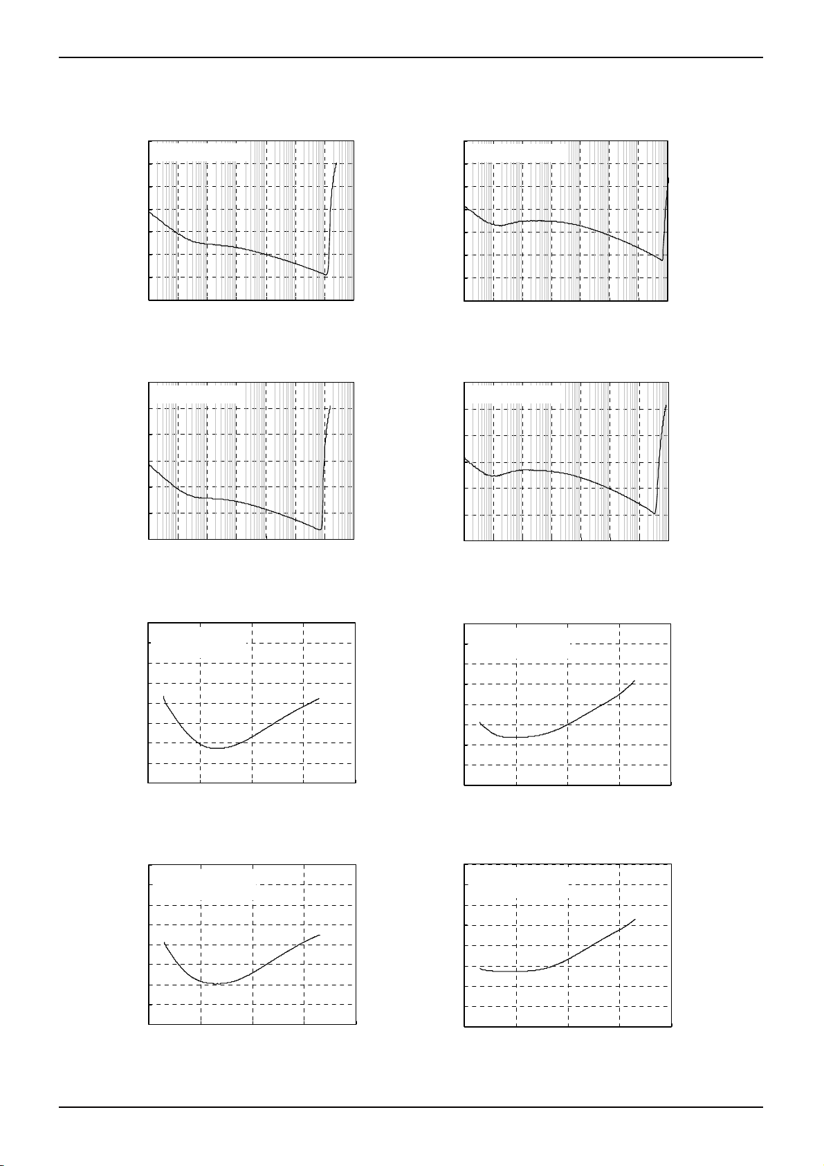
●Electrical characteristics waveform (Reference data)
Ta=25°C, f=1kHz, VSS=GND unless otherwise specified. Using circuits are Fig.34 and Fig.35.
Also, RL=16Ω for single ended mode, RL=8Ω for BTL mode
0
VDD=1.5V, SE mode
-10
-20
-30
-40
THD+N [dB]
-50
-60
-70
10n 100n 1u 10u 100u 1m 10m 100m
Ou tput P o w er [W]
Fig. 2 THD+N vs. Output Power
)
0
VDD=1.5V, BTL mode
-10
-20
-30
-40
THD+N [dB]
-50
-60
-70
10n 100n 1u 10u 100u 1m 10m 100m
Ou tput P o w er [W]
Fig. 3 THD+N vs. Output Power
0
VDD=1.2V, SE mode
-10
-20
-30
THD +N [dB ]
-40
-50
-60
10n 100n 1u 10u 100u 1m 10m 100m
Ou tput P o w er [W]
Fig. 4 THD+N vs. Output Power
0
VDD=1.2V, BTL mode
-10
-20
-30
THD+N [dB]
-40
-50
-60
10n 100n 1u 10u 100u 1m 10m 100m
Ou tput P o w er [W]
Fig. 5 THD+N vs. Output Power
0
VDD=1.5V, Po=5mW,
-10
SE mo de, BW<80kHz
-20
-30
-40
-50
THD+N [dB]
-60
-70
-80
10 100 1k 10k 100k
Frequency [Hz]
Fig. 6 THD+N vs. Frequency
0
VDD=1.5V, Po=25mW,
-10
BTL mode, BW<80kHz
-20
-30
-40
-50
THD+N [dB]
-60
-70
-80
10 100 1k 10k 100k
Frequency [Hz]
Fig. 7 THD+N vs. Frequency
0
VDD=1.2V, Po=2.5mW,
-10
SE mo de, BW<80kHz
-20
-30
-40
-50
THD+N [dB]
-60
-70
-80
10 100 1k 10k 100k
Frequency [Hz]
Fig. 8 THD+N vs. Frequency
0
VDD=1.2V, Po=10mW,
-10
BTL mode, BW<80kHz
-20
-30
-40
-50
THD+N [dB]
-60
-70
-80
10 100 1k 10k 100k
Frequency [Hz]
Fig. 9 THD+N vs. Frequency
Technical Note
www.rohm.com
© 2011 ROHM Co., Ltd. All rights reserved.
3/16
2011.05 - Rev.C

BU7150NUV
0
-10
-20
-30
-40
-50
-60
-70
Outpu t Lev el [dBV]
-80
-90
-100
-100 -80 -60 -40 -2 0 0
0
-20
-40
-60
-80
Ou tput L eve l [d BV]
-100
-120
-120 -100 -80 -60 -4 0 -20 0
10
0
-10
-20
Gain [dB]
-30
-40
-50
10 100 1k 10k 100k 1M
10
0
-10
-20
Gain [dB]
-30
-40
-50
10 100 1k 10k 100k 1M
VDD=1.5V, SE mode
Inp ut Le vel [dBV]
Fig. 10 Output Level vs. Input Level
VDD=1.2V, SE mode
Inp ut Le vel [dBV]
Fig. 12 Output Level vs. Input Level
VDD=1.5V, Po=5mW, SE mode
Frequency [Hz]
Fig. 14 Gain vs. Frequency
VDD=1.2V, Po=2.5m W, SE m ode
Frequency [Hz]
Fig. 16 Gain vs. Frequency
0
-10
VDD=1.5V, BTL mode
-20
-30
-40
-50
-60
-70
Outpu t Lev el [dBV]
-80
-90
-100
-100 -80 -60 -4 0 -20 0
Input Level [dBV]
Fig. 11 Output Level vs. Input Level
0
VDD=1.2V, BTL mode
-20
-40
-60
-80
Outpu t Lev el [dBV]
-100
-120
-120 -100 -80 -60 -40 -2 0 0
Inp u t L evel [dBV]
Fig. 13 Output Level vs . Input Level
10
0
-10
-20
Gain [dB]
-30
-40
VDD=1.5V, Po=25mW, BTL m ode
-50
10 100 1k 10k 100k 1M
10
0
-10
-20
Gain [dB]
-30
-40
VDD=1.2V, Po=10mW, BTL m ode
-50
10 100 1k 10k 100k 1M
Frequency [Hz]
Fig. 15 Gain vs. Frequency
Frequency [Hz]
Fig. 17 Gain vs. Frequency
Technical Note
www.rohm.com
© 2011 ROHM Co., Ltd. All rights reserved.
4/16
2011.05 - Rev.C

BU7150NUV
140
120
100
80
60
Power [mW]
40
20
0
Fig. 18 Maximum output Power vs. Supply Voltage
40
35
30
25
20
15
Power [mW]
10
5
0
0.0 0.5 1.0 1.5 2.0
Fig. 20 Maximum output Power vs. Supply Voltage
0
-10
-20
-30
-40
-50
PSRR [dB]
-60
-70
-80
-90
10 100 1k 10k 100k
0
-10
-20
-30
-40
-50
PSRR [dB]
-60
-70
-80
-90
10 100 1k 10k 100k
SE mo de
THD+N = 10%
THD+N = 1%
01234
SE mode
Zoom up
SE m o de, In put Term ina te d i n to 1 0Ω
SE m ode , In p ut Term ina te d in to 10 Ω
Supply Voltage [V]
THD+N = 10%
Supply Voltage [V]
VDD=1.5V, Input=200mV
Frequency [Hz]
Fig. 22 PSRR vs. Frequency
VDD=1.2V, Input=200mV
Frequency [Hz]
Fig. 24 PSRR vs. Frequency
THD+N = 1%
,
P-P
,
P-P
Technical Note
1000
900
BTL mode
800
700
600
500
400
Power [mW]
300
200
100
0
01234
Fig. 19 Maxim um output Power vs . Supply Voltage
200
BTL mode
180
Zoom up
160
140
120
100
80
Power [mW]
60
40
20
0
0.0 0.5 1.0 1.5 2.0
Fig. 21 Maxim um output Power vs . Supply Voltage
0
-10
-20
-30
-40
-50
PSRR [dB]
-60
-70
-80
-90
-10
-20
-30
-40
-50
PSRR [dB]
-60
-70
-80
-90
VDD=1.5V, Input=200mV
BTL m od e, Inp u t Te rm i nate d in to 10 Ω
10 100 1k 10k 100k
0
VDD=1.2V, Input=200mV
BTL m od e, Inp u t Te rm i nate d in to 10 Ω
10 100 1k 10k 100k
THD+N = 10%
THD+N = 1%
Supply Voltage [V]
THD+N = 10%
THD+N = 1%
Supply Voltage [V]
,
P-P
Frequency [Hz]
Fig. 23 PSRR vs. Frequency
,
P-P
Frequency [Hz]
Fig. 25 PSRR vs. Frequency
:WC (PO=7 0 m W
×
TH D+N =1% )
www.rohm.com
© 2011 ROHM Co., Ltd. All rights reserved.
5/16
2011.05 - Rev.C

BU7150NUV
Crosstalk [dB]
-100
-110
-120
Noise Level [dBV]
-100
-120
-140
-160
-40
-50
-60
-70
-80
-90
-20
-40
-60
-80
VDD=1.5V, Input=400mV
SE mode, Input Terminated into 10Ω
10 100 1k 10k 100k
0
VDD=1.5V, SE mode, 20kHz LPF + A-weight
10 100 1k 10k 100k
Fig. 28 Noise Level vs. Frequency
Frequency [Hz]
Fig. 26 Crosstalk vs. Frequency
Frequency [Hz]
,
P-P
-40
VDD=1.2V, Input=400mV
SE m o de, In put Term ina te d i n to 1 0Ω
10 100 1k 10k 100k
0
VDD=1.5V, BTL mode, 20kHz LPF + A-weight
10 100 1k 10k 100k
Frequency [Hz]
Fig. 27 Crosstalk vs . Frequency
Frequency [Hz]
Fig. 29 Noise Level vs. Frequency
Crosstalk [dB]
Noise Level [dBV]
-50
-60
-70
-80
-90
-100
-110
-120
-20
-40
-60
-80
-100
-120
-140
-160
,
P-P
Technical Note
1.2
SE m o de, In put= no s ign al
1
0.8
0.6
IDD [m A ]
0.4
0.2
0
01234
-50
VDD=1.5V, Input=400mV
-55
-60
-65
-70
-75
MU TE L eve l [dB]
-80
-85
-90
10 100 1k 10k 100k
Supply Voltage [V]
Fig . 3 0 ID D vs. Su p ply Vol ta g e
, SE mode
P-P
Frequem cy [Hz]
Fig. 32 MUTE Level vs. Frequency
4.5
SE m ode , In p ut=n o s i gna l
4
3.5
3
2.5
2
ISD [μA]
1.5
1
0.5
0
01234
Supply Voltage [V]
Fig. 31 ISD vs. Supply Voltage
www.rohm.com
© 2011 ROHM Co., Ltd. All rights reserved.
6/16
2011.05 - Rev.C

BU7150NUV
●Application Circuit
+
+
+
・Resistors R
, RF2 should be used in 20kΩ~1MΩ range.
F1
・For gain setting greater than 4 times, then R
Fig. 34 Single-ended mode application circuit
+
+
・Resistors R
, RF2 should be used in 20kΩ~1MΩ range
F1
Fig. 35 BTL mode application circuit
, RC2, CC1, CC2 can be eliminated.
C1
Technical Note
++
www.rohm.com
© 2011 ROHM Co., Ltd. All rights reserved.
7/16
2011.05 - Rev.C

BU7150NUV
●Pin Configuration
No.
Pin Name Function I/O equal circuit
1 IN1 Input Pin 1 A
2 SDB Shutdown Pin (OFF at L) C
3 MUTEB Mute Pin (Mute at L) C
4 BYPASS Bypass Pin D
5 IN2 Input Pin 2 A
6 VSS GND Pin -
7 OUT2 Output Pin 2 B
8 MODE Mode Select Pin (SE at VSS, BTL at VDD) A
9 OUT1 Output Pin 1 B
10 VDD Power Supply Pin -
●I/O equal circuit (Fig. 36)
IN1
IN2
MODE
VDD
50Ω
VDD
Technical Note
VDDVDD
OUT1
OUT2
A B
SDB
MUTEB
VDD
2kΩ
C
BYPASS
VDD
VDD
D
VDD
600kΩ
Fig.36 I/O equal circuit
100kΩ
100kΩ
www.rohm.com
© 2011 ROHM Co., Ltd. All rights reserved.
8/16
2011.05 - Rev.C

BU7150NUV
●Functional descriptions
[Timing Chart]
BU7150NUV can control many mode states. “Active” is normal operation state for output signal. “Shutdown” is IC power
down state for low power. “Mute” is Headphone amplifier power down state for low power and fast turn-on, because
keeping BIAS voltage = VDD/2. “Turn on” and “Turn off” are sweep state.
Also, BU7150NUV has wait time for reduction of pop-sound at turn-on and turn-off. Turn-on wait time is 70msec from IN1
voltage = VDD/2. Turn-off wait time is 140msec from BYPASS voltage = 100mV. Please don't change SDB, MUTEB
condition at 70msec and 140msec wait- time.
Fig. 37 Timing Chart (MODE = VSS: Single-ended mode)
Fig. 38 Timing Chart (MODE = VDD: BTL- mode)
Technical Note
www.rohm.com
© 2011 ROHM Co., Ltd. All rights reserved.
9/16
2011.05 - Rev.C

BU7150NUV
[About Time until Signal Output]
BU7150NUV need wait-time for BIAS charge sweep time and pop-noise reduction.
In the Fig. 37, Ts1 is BIAS charge sweep time from power on or SDB=H. Ts2 is time until signal output from power on or
SDB=H. Also, in the Fig. 38, Tb1 is BIAS charge sweep time from power on. Tb2 is time until signal output from power on.
Tb3 is BIAS charge sweep time from SDB=H. Tb4 is time until signal output from SDB=H.
These values are decided equation (1) ~ (6). However, BIAS charge sweep time (Ts1, Tb1, Tb3) have uneven ±50%, and
wait-time (70msec) is 40msec ~ 126msec for process parameter distribution. (Ta=25°C)
CVDD
1Ts
1Tb
3Tb
In the Fig. 38, Tb1 and Tb3 is differ value, because BU7150NUV’s default is single-ended mode. BU7150NUV need
BYPASS>100mV to recognize for BTL mode.
Also, Td is delay time to C
BYPASS
6
105.2
C2VDD
BYPASS
105.27
CVDD
BYPASS
6
105.27
=VDD/2 from BYPASS=VDD/2. Td is decided by CI1, RI1, and RF1.
I1
・・・
6
・・・
・・・
)1([sec]
)2([sec]07.01Ts2Ts ・・・
)3([sec]
)4([sec]07.01Tb2Tb ・・・
)5([sec]
)6([sec]07.03Tb4Tb ・・・
Technical Note
Fig. 39 Flow of Time until Signal Output
www.rohm.com
© 2011 ROHM Co., Ltd. All rights reserved.
10/16
2011.05 - Rev.C

BU7150NUV
Technical Note
[Operation mode]
・Selecting operation mode
BU7150NUV has two OPAMP in the IC (Fig. 1). BU7150NUV is selected for BTL-mode for mono speaker and
single-ended mode for stereo headphone operation. Mode is composed of external parts and internal control (Fig. 34, 35)
BU7150NUV operates at single-ended mode when MODE pin (pin8) = 0V turn on. BTL mode is operated when MODE
pin (pin8) = VDD turn on. BYPASS voltage = 100mV then operation mode is decided by internal comparator by detecting
MODE voltage.
The difference between Single-ended mode and BTL-mode is mentioned in the following table.
Parameter
Single ended mode
MODE='VSS'
BTL mode
MODE='VDD'
Mute function
Bypass voltage turn on time [Ts1, Tb1, Tb3]
(C
BYPASS
=4.7μF)
Time until Signal Output [Ts2, Tb2,
BYPASS
=4.7μF)
Tb4](C
Maximum Output Power (THD=1%)
Total Harmonic Distortion + Noise
Power Supply Rejection Ratio
(Ta=25℃, VDD=1.5V, f=1kHz)
Ts1=2.82sec
Ts2=2.89sec
disenable
enable
Tb1=598msec
Tb3=256msec
Tb1=668msec
Tb3=326msec
14mW 85mW
0.10% 0.20%
66dB 62dB
www.rohm.com
© 2011 ROHM Co., Ltd. All rights reserved.
11/16
2011.05 - Rev.C

BU7150NUV
・Single-Ended mode
Single-ended mode can be use for stereo headphone amplifier using two internal amplifiers. BU7150NUV can select
amplifier gain A
resistance R
A
V
Amplifier outputs (OUT1, OUT2) need coupling capacitors in single-ended mode operation. Coupling capacitors reduce
DC-voltage at the output and to pass the audio signal.
Single-ended mode has mute mode. Mute mode reduces pop noise and low power (typ. 15μA when MUTEB pin = Low.
Rise time is high-speed though current consumption increases more than the state of the shutdown so that the state of
the mute may keep the output level at the bias level. Mute level is decided by input resistance R
resistance R
Mute level [dB]
BU7150NUV needs phase-compensation circuit using external parts. (Fig. 34) But, for amplifier gain Av > 4 then phase
compensation circuit may be eliminated.
・BTL mode
BTL mode can be used for mono speaker amplifier using two internal amplifiers. BU7150NUV can select amplifier gain A
using external parts. (Fig. 35) 1st stage gain is decided by selecting external parts. But 2nd stage gain = 1. 1st stage
output signal and 2nd stage output signal are of same amplitude but phase difference of 180°.
Amplifiers gain A
in range of 20kΩ~1MΩ.
V
BU7150NUV has no output pop noise at BTL mode operation, because output coupling capacitor is not charged.
Therefore, BTL mode is faster by 11 times compared to single-ended mode. SDB pin and MUTEB pin are same function
in BTL mode operation.
using external parts. (Fig. 34) Two amplifiers gain Av is decided by input resistance RI1, RI2 and feedback
v
, RF2 aspect. Also, Please, use RF1, RF2 value in the range 20kΩ~1MΩ.
F1
R
F
R
I
, RF2 and RL
F1
R
Log20
is decided by input resistance RI1 and feedback resistance RF1 aspect. Also, Please, use RF1, RF2 value
v
R
1F
2A
R
1I
L
RR
FI
Technical Note
, RI2 and feedback
I1
v
www.rohm.com
© 2011 ROHM Co., Ltd. All rights reserved.
12/16
2011.05 - Rev.C
BU7150NUV
Technical Note
[About Maximum Output Power]
Maximum output power of audio amplifier is reduced line impedance. Please, design to provide low impedance for the
wiring between the power source and VDD pin of BU7150NUV. Also, please design to provide low impedance for the
wiring between the GND and VSS pin of BU7150NUV.
VDD
Power source
Impedance
Speaker
Impedance
GND
Impedance
Fig. 40 Line Impedance
www.rohm.com
© 2011 ROHM Co., Ltd. All rights reserved.
13/16
2011.05 - Rev.C

BU7150NUV
Technical Note
[How to select external parts for application]
・Power supply capacitor
Power supply capacitor is important for low noise and rejection of alternating current. Please use 10μF electrolytic or
tantalum capacitor for low frequency and 0.1μF ceramic capacitor for high frequency nearer to BU7150NUV.
・BYPASS pin capacitor
BU7150NUV sweeps “Active” state after 70msec wait time after IN1 voltage = VDD/2. IN1 voltage are subordinated
BYPASS voltage Ts. BYPASS voltage is subordinated BYPASS pin capacitor C
is possible if C
is small value. But, pop noise may occur during turn on time. Therefore, C
BYPASS
. Therefore, High speed turn on time
BYPASS
need to be selected
BYPASS
best value for application.
www.rohm.com
© 2011 ROHM Co., Ltd. All rights reserved.
14/16
2011.05 - Rev.C

BU7150NUV
●Notes for use
(1) Absolute Maximum Ratings
An excess in the absolute maximum ratings, such as supply voltage, temperature range of operating conditions, etc.,
can break down devices, thus making impossible to identify breaking mode such as a short circuit or an open circuit. If
any special mode exceeding the absolute maximum ratings is assumed, consideration should be given to take physical
safety measures including the use of fuses, etc.
(2) Operating conditions
These conditions represent a range within which characteristics can be provided approximately as expected. The
electrical characteristics are guaranteed under the conditions of each parameter.
(3) Reverse connection of power supply connector
The reverse connection of power supply connector can break down ICs. Take protective measures against the
breakdown due to the reverse connection, such as mounting an external diode between the power supply and the IC’s
power supply terminal.
(4) Power supply line
Design PCB pattern to provide low impedance for the wiring between the power supply and the GND lines. In this
regard, for the digital block power supply and the analog block power supply, even though these power supplies has
the same level of potential, separate the power supply pattern for the digital block from that for the analog block, thus
suppressing the diffraction of digital noises to the analog block power supply resulting from impedance common to the
wiring patterns. For the GND line, give consideration to design the patterns in a similar manner.
Furthermore, for all power supply terminals to ICs, mount a capacitor between the power supply and the GND terminal.
At the same time, in order to use an electrolytic capacitor, thoroughly check to be sure the characteristics of the
capacitor to be used present no problem including the occurrence of capacity dropout at a low temperature, thus
determining the constant.
(5) GND voltage
Make setting of the potential of the GND terminal so that it will be maintained at the minimum in any operating state.
Furthermore, check to be sure no terminals are at a potential lower than the GND voltage including an actual electric
transient.
(6) Short circuit between terminals and erroneous mounting
In order to mount ICs on a set PCB, pay thorough attention to the direction and offset of the ICs. Erroneous mounting
can break down the ICs. Furthermore, if a short circuit occurs due to foreign matters entering between terminals or
between the terminal and the power supply or the GND terminal, the ICs can break down.
(7) Operation in strong electromagnetic field
Be noted that using ICs in the strong electromagnetic field can malfunction them.
(8) Inspection with set PCB
On the inspection with the set PCB, if a capacitor is connected to a low-impedance IC terminal, the IC can suffer stress.
Therefore, be sure to discharge from the set PCB by each process. Furthermore, in order to mount or dismount the set
PCB to/from the jig for the inspection process, be sure to turn OFF the power supply and then mount the set PCB to
the jig. After the completion of the inspection, be sure to turn OFF the power supply and then dismount it from the jig. In
addition, for protection against static electricity, establish a ground for the assembly process and pay thorough attention
to the transportation and the storage of the set PCB.
(9) Input terminals
In terms of the construction of IC, parasitic elements are inevitably formed in relation to potential. The operation of the
parasitic element can cause interference with circuit operation, thus resulting in a malfunction and then breakdown of
the input terminal. Therefore, pay thorough attention not to handle the input terminals, such as to apply to the input
terminals a voltage lower than the GND respectively, so that any parasitic element will operate. Furthermore, do not
apply a voltage to the input terminals when no power supply voltage is applied to the IC. In addition, even if the power
supply voltage is applied, apply to the input terminals a voltage lower than the power supply voltage or within the
guaranteed value of electrical characteristics.
(10) Ground wiring pattern
If small-signal GND and large-current GND are provided, It will be recommended to separate the large-current GND
pattern from the small-signal GND pattern and establish a single ground at the reference point of the set PCB so that
resistance to the wiring pattern and voltage fluctuations due to a large current will cause no fluctuations in voltages of
the small-signal GND. Pay attention not to cause fluctuations in the GND wiring pattern of external parts as well.
(11) External capacitor
In order to use a ceramic capacitor as the external capacitor, determine the constant with consideration given to a
degradation in the nominal capacitance due to DC bias and changes in the capacitance due to temperature, etc.
(12) About the rush current
For ICs with more than one power supply, it is possible that rush current may flow instantaneously due to the internal
powering sequence and delays. Therefore, give special consideration to power coupling capacitance, power wiring,
width of GND wiring, and routing of wiring.
(13) Others
In case of use this LSI, please peruse some other detail documents, we called ,Technical note, Functional description,
Application note.
Technical Note
www.rohm.com
© 2011 ROHM Co., Ltd. All rights reserved.
15/16
2011.05 - Rev.C

BU7150NUV
●Ordering part number
B D 7 1 5 0 N U V - E 2
Part No. Part No.
VSON010V3030
3.0±0.1
0.08
1.0MAX
S
2.0±0.1
C0.25
0.4±0.1
0.5
1PIN MARK
0.5
51
610
0.25
3.0±0.1
0.02
+0.03
-
0.02
1.2±0.1
+0.05
-
S
(0.22)
0.04
(Unit : mm)
Package
NUV : VSON010V3030
<Tape and Reel information>
Embossed carrier tapeTape
Quantity
Direction
of feed
3000pcs
E2
The direction is the 1pin of product is at the upper left when you hold
()
reel on the left hand and you pull out the tape on the right hand
Reel
1pin
Packaging and forming specification
E2: Embossed tape and reel
Order quantity needs to be multiple of the minimum quantity.
∗
Technical Note
Direction of feed
www.rohm.com
© 2011 ROHM Co., Ltd. All rights reserved.
16/16
2011.05 - Rev.C

Notes
No copying or reproduction of this document, in part or in whole, is permitted without the
consent of ROHM Co.,Ltd.
The content specied herein is subject to change for improvement without notice.
The content specied herein is for the purpose of introducing ROHM's products (hereinafter
"Products"). If you wish to use any such Product, please be sure to refer to the specications,
which can be obtained from ROHM upon request.
Examples of application circuits, circuit constants and any other information contained herein
illustrate the standard usage and operations of the Products. The peripheral conditions must
be taken into account when designing circuits for mass production.
Great care was taken in ensuring the accuracy of the information specied in this document.
However, should you incur any damage arising from any inaccuracy or misprint of such
information, ROHM shall bear no responsibility for such damage.
The technical information specied herein is intended only to show the typical functions of and
examples of application circuits for the Products. ROHM does not grant you, explicitly or
implicitly, any license to use or exercise intellectual property or other rights held by ROHM and
other parties. ROHM shall bear no responsibility whatsoever for any dispute arising from the
use of such technical information.
The Products specied in this document are intended to be used with general-use electronic
equipment or devices (such as audio visual equipment, ofce-automation equipment, communication devices, electronic appliances and amusement devices).
The Products specied in this document are not designed to be radiation tolerant.
While ROHM always makes efforts to enhance the quality and reliability of its Products, a
Product may fail or malfunction for a variety of reasons.
Please be sure to implement in your equipment using the Products safety measures to guard
against the possibility of physical injury, re or any other damage caused in the event of the
failure of any Product, such as derating, redundancy, re control and fail-safe designs. ROHM
shall bear no responsibility whatsoever for your use of any Product outside of the prescribed
scope or not in accordance with the instruction manual.
The Products are not designed or manufactured to be used with any equipment, device or
system which requires an extremely high level of reliability the failure or malfunction of which
may result in a direct threat to human life or create a risk of human injur y (such as a medical
instrument, transportation equipment, aerospace machinery, nuclear-reactor controller, fuelcontroller or other safety device). ROHM shall bear no responsibility in any way for use of any
of the Products for the above special purposes. If a Product is intended to be used for any
such special purpose, please contact a ROHM sales representative before purchasing.
If you intend to export or ship overseas any Product or technology specied herein that may
be controlled under the Foreign Exchange and the Foreign Trade Law, you will be required to
obtain a license or permit under the Law.
Notice
www.rohm.com
© 2011 ROHM Co., Ltd. All rights reserved.
Thank you for your accessing to ROHM product informations.
More detail product informations and catalogs are available, please contact us.
ROHM Customer Support System
http://www.rohm.com/contact/
R1120
A
 Loading...