

Hall IC Series / Hall IC(Latch type)
Bipolar Detection Hall ICs
BU52001GUL, BU52011HFV, BU52021HFV,
BU52015GUL, BU52025G, BU52051NVX, BD7411G
٨Description
The bipolar Hall ICs are magnetic switches that can operate both S-and N-pole , upon which the output goes from Hi to Low.
In addition to regular single-output Hall ICs, We offers a line up of dual-output units with a reverse output terminal (active
High).
٨Features
1) Bipolar detection
2) Micropower operation (small current using intermittent operation method)(BD7411G is excluded.)
3) Ultra-compact CSP4 package (BU52001GUL,BU52015GUL)
4) Ultra-Small outline package HVSOF5 (BU52011HFV,BU52021HFV)
5) Ultra-Small outline package SSON004X1216 (BU52051NVXV)
6) Small outline package (BU52025G,BD7411G㧕
7) Line up of supply voltage
For 1.8V Power supply voltage㧔BU52011HFV,BU52015GUL,BU52051NVX)
For 3.0V Power supply voltage (BU52001GUL)
For 3.3V Power supply voltage (BU52021HFV,BU52025G)
For 5.0V Power supply voltage (BD7411G)
8) Dual output type (BU52015GUL)
9) High ESD resistance 8kV(HBM)
٨Applications
Mobile phones, notebook computers, digital video camera, digital still camera, white goods etc.
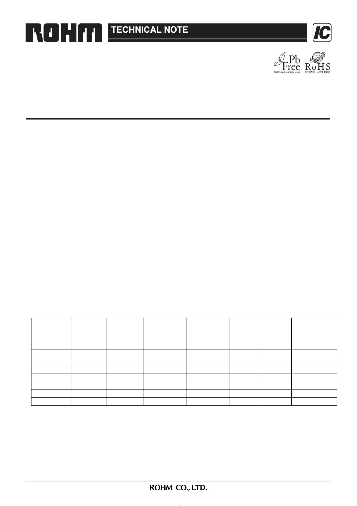
٨Product Lineup
Supply
Product name
BU52001GUL 2.40㨪3.30 +/-3.7 0.8 50 8.0㱘 CMOS VCSP50L1
BU52015GUL 1.65㨪3.30 +/-3.0 0.9 50 5.0㱘 CMOS VCSP50L1
BU52051NVX 1.65㨪3.30 +/-3.0 0.9 50 5.0㱘 CMOS SSON004X1216
BU52011HFV 1.65㨪3.30 +/-3.0 0.9 50 5.0㱘 CMOS HVSOF5
BU52021HFV 2.40㨪3.60 +/-3.7 0.8 50 8.0㱘 CMOS HVSOF5
BU52025G 2.40㨪3.60 +/-3.7 0.8 50 8.0㱘 CMOS SSOP5
BD7411G 4.50㨪5.50 +/-3.4 0.4 - 2.0m CMOS SSOP5
㶎Plus is expressed on the S-pole; minus on the N-pole
voltage
(V)
Operate
point
(mT)
Hysteresis
(mT)
Period
(ms)
Supply
current
(AVG)
(A)
Output
type
Package
Jul. 2008
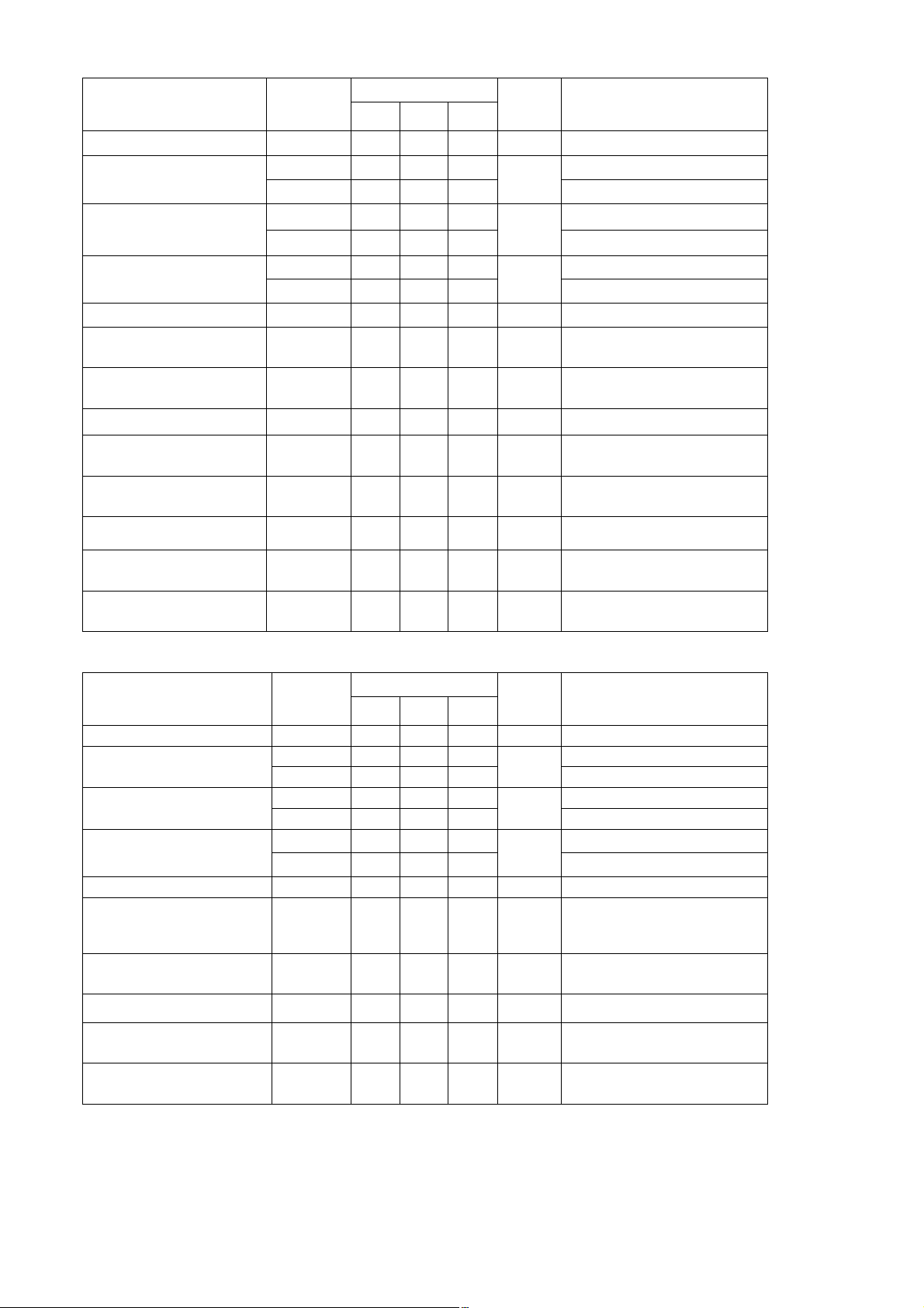
٨Absolute Maximum Ratings
BU52001GUL (Ta=25㷄) BU52015GUL (Ta=25㷄)
PARAMETERS SYMBOL LIMIT UNIT PARAMETERS SYMBOL LIMIT UNIT
1
Power Supply Voltage
Output Current
V
I
OUT
Power Dissipation Pd
Operating Temperature Range T
Storage Temperature Range T
DD
opr
stg
-0.1㨪+4.5
r1
2
420
-40㨪+85
-40㨪+125
㶎1. Not to exceed Pd
㶎2. Reduced by 4.20mW for each increase in Ta of 1㷄 over 25㷄
䋨mounted on 50mm㬍58mm Glass-epoxy PCB䋩
V
mA
mW
Power Supply Voltage
Output Current
Power Dissipation Pd
Operating Temperature Range T
Storage Temperature Range T
㶎3. Not to exceed Pd
㶎4. Reduced by 4.20mW for each increase in Ta of 1㷄 over 25㷄
䋨mounted on 50mm㬍58mm Glass-epoxy PCB䋩
BU52051NVX (Ta=25㷄) BU52011HFV (Ta=25㷄)
PARAMETERS SYMBOL LIMIT UNIT PARAMETERS SYMBOL LIMIT UNIT
5
Power Supply Voltage
Output Current
V
I
OUT
Power Dissipation Pd
Operating Temperature Range T
Storage Temperature Range T
DD
-0.1㨪+4.5
r0.5
6
2049
opr
stg
-40㨪+85
-40㨪+125
V
mA
mW
Power Supply Voltage
Output Current
Power Dissipation Pd
Operating Temperature Range T
Storage Temperature Range T
㶎5. Not to exceed Pd
㶎6. Reduced by 20.49mW for each increase in Ta of 1㷄 over 25㷄
䋨mounted on 70mm㬍70 mm㬍1.6mm Glass-epoxy PCB䋩
㶎7. Not to exceed Pd
㶎8. Reduced by 5.36mW for each increase in Ta of 1㷄 over 25㷄
䋨mounted on 70mm㬍70 mm㬍1.6mm Glass-epoxy PCB䋩
BU52021NVX (Ta=25㷄) BU52025G (Ta=25㷄)
PARAMETERS SYMBOL LIMIT UNIT PARAMETERS SYMBOL LIMIT UNIT
9
Power Supply Voltage
V
DD
-0.1㨪+4.5
V
Power Supply Voltage
V
I
V
I
V
OUT
OUT
3
DD
-0.1㨪+4.5
r0.5
4
420
opr
stg
DD
-40㨪+85
-40㨪+125
-0.1㨪+4.5
r0.5
8
536
opr
stg
-40㨪+85
-40㨪+125
-0.1㨪+4.5
DD
11
V
mA
mW
7
V
mA
mW
V
I
Output Current
OUT
Power Dissipation Pd
Operating Temperature Range T
Storage Temperature Range T
opr
stg
r1
10
536
-40㨪+85
-40㨪+125
㶎9. Not to exceed Pd
㶎10. Reduced by5.36mW for each increase in Ta of 1㷄 over 25㷄
䋨mounted on 70mm㬍70 mm㬍1.6mm Glass-epoxy PCB䋩
mA
mW
Output Current
Power Dissipation Pd
Operating Temperature Range T
Storage Temperature Range T
㶎11. Not to exceed Pd
㶎12. Reduced by 5.40mW for each increase in Ta of 1㷄 over 25㷄
䋨mounted on 70mm㬍70 mm㬍1.6mm Glass-epoxy PCB䋩
BD7411G (Ta=25㷄)
PARAMETERS SYMBOL LIMIT UNIT
13
Power Supply Voltage
Output Current
V
I
OUT
Power Dissipation Pd
Operating Temperature Range T
Storage Temperature Range T
DD
opr
stg
-0.3㨪+7.0
-55㨪+150
r1
14
540
-40㨪+85
㶎13. Not to exceed Pd
㶎14. Reduced by 5.40mW for each increase in Ta of 1㷄 over 25㷄
䋨mounted on 70mm㬍70 mm
㬍1.6mm Glass-epoxy PCB䋩
V
mA
mW
I
OUT
r1
12
540
opr
stg
-40㨪+85
-40㨪+125
mA
mW
2/20

٨Magnetic, Electrical Characteristics
BU52001GUL (Unless otherwise specified, V
PARAMETERS SYMBOL
Power Supply Voltage
Operate Point
Release Point
Hysteresis
2.4 3.0 3.3 V
V
DD
B
- 3.7 5.5
opS
B
opN
0.8 2.9 -
B
rpS
B
rpN
B
hysS
B
hysN
䋽3.0V, Ta䋽25㷄) 㩷㩷㩷㩷 㩷㩷㩷㩷㩷
DD
LIMIT
MIN TYP MAX
-5.5 -3.7 -
- -2.9 -0.8
- 0.8 -
- 0.8 -
UNIT CONDITIONS
mT
mT
mT
Period Tp - 50 100 ms
V
Output High Vol䌴age V
OH
DD
-0.4
- - V
Output Low Voltage VOL - - 0.4 V
Supply Current I
Supply Current
During Startup Time
Supply Current
During Standby Time
- 8 12 ǴA Average
DD(AVG)
I
- 4.7 - mA During Startup Time Value
DD(EN)
- 3.8 - 㱘A During Standby Time Value
I
DD(DIS)
B
<B<B
rpN
=-1.0mA
I
OUT
B<B
opN,BopS
=+1.0mA
I
OUT
15
rpS
<B 15
㶎15 B = Magnetic flux density 㩷㩷㩷㩷㩷㩷㩷㩷㩷㩷㩷㩷㩷㩷㩷㩷㩷㩷㩷㩷㩷㩷㩷㩷㩷㩷㩷㩷㩷㩷㩷㩷㩷㩷㩷㩷㩷㩷
1mT=10Gauss
Positive (“+”) polarity flux is defined as the magnetic flux from south pole which is direct toward to
the branded face of the sensor.
After applying power supply, it takes one cycle of period (T
) to become definite output.
P
Radiation hardiness is not designed.
3/20

BU52015GUL (Unless otherwise specified,
PARAMETERS SYMBOL
㪭㪛㪛䋽㪈㪅㪏㪇㪭㪃㩷㪫㪸䋽㪉㪌㷄㪀
LIMIT
MIN TYP MAX
UNIT CONDITIONS
Power Supply Voltage VDD 1.65 1.80 3.30 V
B
- 3.0 5.0
Operate Point
Release Point
opS
mT
B
-5.0 -3.0 -
opN
B
0.6 2.1 -
rpS
mT
B
- -2.1 -0.6
rpN
Hysteresis
B
hysS
B
hysN
- 0.9 mT
- 0.9 -
Period Tp - 50 100 ms
OUT1: B
OUT2: B<B
I
Output High Vol䌴age V
OH
V
DD
-0.2
- - V
OUT1: B<B
Output Low Voltage VOL - - 0.2 V
OUT2: B
I
Supply Current 1 I
Supply Current
During Startup Time 1
Supply Current
During Standby Time 1
Supply Current 2 I
Supply Current
During Startup Time 2
Supply Current
During Standby Time 2
DD1(AVG)
I
DD1(EN)
I
DD1(DIS)
DD2(AVG)
I
DD2(EN)
I
DD2(DIS)
- 5 8 㱘A VDD=1.8V, Average
- 2.8 - mA
- 1.8 - 㱘A
VDD=1.8V,
During Startup Time Value
VDD=1.8V,
During Standby Time Value
- 8 12 㱘A VDD=2.7V, Average
- 4.5 - mA
- 4.0 - 㱘A
VDD=2.7V,
During Startup Time Value
V
During Standby Time Value
OUT
OUT
DD
=2.7V,
<B<B
rpN
opN
= -0.5mA
opN
<B<B
rpN
= +0.5mA
, B
, B
rpS
opS
opS
rpS
㶎16 B = Magnetic flux density 㩷㩷㩷㩷㩷㩷㩷㩷㩷㩷㩷㩷㩷㩷㩷㩷㩷㩷㩷㩷㩷㩷㩷㩷㩷㩷㩷㩷㩷㩷㩷㩷㩷㩷㩷㩷㩷㩷
1mT=10Gauss
Positive (“+”) polarity flux is defined as the magnetic flux from south pole which is direct toward to
the branded face of the sensor.
After applying power supply, it takes one cycle of period (T
) to become definite output.
P
Radiation hardiness is not designed.
16
㩷㩷㩷 㩷
<B
<B 16
4/20
BU52051NVX , BU52011HFV (Unless otherwise specified, V
LIMIT
PARAMETERS SYMBOL
MIN TYP MAX
䋽1.80V, Ta䋽25㷄)㩷㩷
DD
UNIT CONDITIONS
Power Supply Voltage VDD 1.65 1.80 3.30 V
Operate Point
Release Point
Hysteresis
opS
B
-5.0 -3.0 -
opN
B
0.6 2.1 -
rpS
B
- -2.1 -0.6
rpN
- 0.9 -
B
hysS
B
- 0.9 -
hysN
mT
mT
mT
- 3.0 5.0
B
Period Tp - 50 100 ms
Output High Vol䌴age V
OH
DD
-0.2
- - V
V
Output Low Voltage VOL - - 0.2 V
Supply Current 1 I
Supply Current
During Startup Time 1
Supply Current
During Standby Time 1
Supply Current 2 I
Supply Current
During Startup Time 2
Supply Current
During Standby Time 2
DD1(AVG)
I
DD1(EN)
I
DD1(DIS)
DD2(AVG)
I
DD2(EN)
I
DD2(DIS)
- 5 8 㱘A VDD=1.8V, Average
-
-
-
-
2.8
1.8
-
8
4.5
4.0
- mA
- 㱘A
12 㱘A VDD=2.7V, Average
- mA
- 㱘A
B
<B<B
rpN
=-0.5mA
I
OUT
B<B
opN
=+0.5mA
I
OUT
V
=1.8V,
DD
17
rpS
, B
<B17
opS
During Startup Time Value
VDD=1.8V,
During Standby Time Value
VDD=2.7V,
During Startup Time Value
V
=2.7V,
DD
During Standby Time Value
BU52021HFV,BU52025G (Unless otherwise specified, VDD䋽3.0V, Ta䋽25㷄) 㩷㩷㩷㩷㩷㩷㩷㩷㩷㩷㩷
PARAMETERS SYMBOL
MIN TYP MAX
LIMIT
UNIT CONDITIONS
Power Supply Voltage VDD 2.4 3.0 3.6 V
B
- 3.7 5.5
Operate Point
Release Point
Hysteresis
opS
B
-5.5 -3.7 -
opN
B
0.8 2.9 -
rpS
B
- -2.9 -0.8
rpN
B
hysS
B
hysN
- 0.8 -
- 0.8 -
mT
mT
mT
Period Tp - 50 100 ms
Output High Vol䌴age V
OH
DD
-0.4
- - V
V
Output Low Voltage VOL - - 0.4 V
I
Supply Current
Supply Current
During Startup Time
Supply Current
During Standby Time
DD(AVG)
I
-
DD(EN)
I
-
DD(DIS)
-
8
4.7
3.8
12 ǴA Average
- mA During Startup Time Value
- 㱘A During Standby Time Value
B
<B<B
rpN
=-1.0mA
I
OUT
B<B
opN
=+1.0mA
I
OUT
17
rpS
, B
<B 17
opS
㶎17 B = Magnetic flux density 㩷㩷㩷㩷㩷㩷㩷㩷㩷㩷㩷㩷㩷㩷㩷㩷㩷㩷㩷㩷㩷㩷㩷㩷㩷㩷㩷㩷㩷㩷㩷㩷㩷㩷㩷㩷㩷㩷
1mT=10Gauss
Positive (“+”) polarity flux is defined as the magnetic flux from south pole which is direct toward to
the branded face of the sensor.
After applying power supply, it takes one cycle of period (T
) to become definite output.
P
Radiation hardiness is not designed.
5/20

BD7411G (Unless otherwise specified, V
PARAMETERS SYMBOL
䋽5.0V, Ta䋽25㷄)
DD
LIMIT
MIN TYP MAX
UNIT CONDITIONS
Power Supply Voltage V
Operate Point
Release Point
B
Hysteresis
B
Output High Vol䌴age V
Output Low Voltage V
Supply Current I
B
B
B
B
DD
opS
opN
rpS
rpN
hysS
hysN
OH
OL
DD
4.5 5.0 5.5
- 3.4 5.6
-5.6 -3.4 -
1.5 3.0 -
- -3.0 -1.5
- 0.4 -
- 0.4 -
4.6
- -
- - 0.4
- 2 4
V
mT
mT
mT
B
V
V
rpN
I
OUT
B<B
I
OUT
mA
<B<B
rpS
=-1.0mA
, B
opN
opS
=+1.0mA
18
<B 18
㶎18 B = Magnetic flux density 㩷㩷㩷㩷㩷㩷㩷㩷㩷㩷㩷㩷㩷㩷㩷㩷㩷㩷㩷㩷㩷㩷㩷㩷㩷㩷㩷㩷㩷㩷㩷㩷㩷㩷㩷㩷㩷㩷
1mT=10Gauss
Positive (“+”) polarity flux is defined as the magnetic flux from south pole which is direct toward to
the branded face of the sensor.
Radiation hardiness is not designed.
6/20

٨Figure of measurement circuit
Bop/B
rp
T
p
200ǡ
VDD
VDD
100ǴF
OUT
GND
Bop and Brp are measured with applying the magnetic field
from the outside.
Fig.1 Bop,Brp measurement circuit
V
OH
VDD
VDD
Fig.3 V
100ǴF
measurement circuit
OH
OUT
GND
VDD
Oscilloscope
OUT
GND
V
The period is monitored by Oscilloscope.
VDD
Fig.2 T
measurement circuit
p
Product Name I
OUT
BU52001GUL, BU52021HFV, BU52025G, BD7411G 1.0mA
BU52015GUL, BU52051NVX, BU52011HFV 0.5mA
I
V
OUT
V
OL
VDD
I
DD
VDD
Fig.4 V
A
100ǴF
measurement circuit
OL
C
VDD
GND
VDD
GND
OUT
OUT
Product Name I
OUT
BU52001GUL, BU52021HFV, BU52025G, BD7411G 1.0mA
BU52015GUL, BU52051NVX, BU52011HFV 0.5mA
V
I
OUT
Product Name C
BU52001GUL,BU52015GUL,BU52051NVX,
2200㱘F
BU52011HFV, BU52021HFV, BU52025G
BD7411G
100㱘F
Fig.5 IDDmeasurement circuit
7/20

٨ Technical (Reference) Data
BU52001GUL (V
8.0
6.0
4.0
2.0
0.0
-2.0
-4.0
-6.0
MAGNETIC FLUX DENSITY [mT]
-8.0
-60 - 40 - 20 0 20 40 60 80 100
=2.4V㨪3.3V type)
DD
V
=3.0V㩷
DD
AMBI ENT TEMPER ATURE [㷄]
Bop S
Brp S
Brp N
Bop N
Fig.6 Bop,Brp–
Ambient temperature
8.0
6.0
Ta = 25°C
4.0
2.0
0.0
-2.0
-4.0
-6.0
MAGNETIC FLUX DENSITY [mT]
-8.0
2.02.4 2.83.23.6
SUPPLY VOLT AGE 䌛V
Bop S
Brp S
Brp N
Bop N
䌝
Fig.7 Bop,Brp– Supply voltage
100
90
VDD=3.0V
80
70
60
50
40
PERIOD [ms]
30
20
10
0
-60 - 40 - 20 0 20 40 60 80 100
AMBIEN T TEMPERATUR E [㷄]
Fig.8 T
– Ambient
P
temperature
100
90
Ta = 25°C
80
70
60
50
40
PERIOD [ms]
30
20
10
0
2.0 2. 4 2.8 3. 2 3.6
SUPPLY VOLTAGE [V]
Fig.9 TP– Supply voltage
BU52015GUL, BU52051NVX, BU52011HFV (V
8.0
6.0
=1.8V
V
DD
4.0
2.0
0.0
-2.0
-4.0
-6.0
MAGNETIC FLUX DENSITY [mT]
-8.0
- 60 - 40 - 20 0 20 40 60 80 100
AMBIENT TEM PERAT UR E [㷄]
Bop S
Brp S
Brp N
Bop N
Fig.12 Bop,Brp–
Ambient temperature
14.0
12.0
VDD=3.0V
10.0
8.0
6.0
4.0
2.0
0.0
AVERAGE SUPPLY CURRENT [µA]
-60 -40 -20 0 20 40 60 80 100
AMBIEN T TEMPERATUR E [㷄]
Fig.10 I
– Ambient
DD
temperature
=1.65V㨪3.3V type)
DD
8.0
6.0
Ta = 25°C
4.0
2.0
0.0
-2.0
-4.0
-6.0
MAGNETIC FLUX DENSITY [mT]
-8.0
㪈㪅㪋 㪈㪅 㪏 㪉㪅 㪉 㪉㪅㪍 㪊㪅 㪇 㪊㪅 㪋 㪊㪅㪏
SUPPLY VOLT AGE 䌛V
Bop S
Brp S
Brp N
Bop N
䌝
Fig.13 Bop,Brp– Supply voltage
14.0
12.0
Ta = 25°C
10.0
8.0
6.0
4.0
2.0
AVERAGE SUPPLY CURRENT [µA]
0.0
2.0 2.4 2.8 3.2 3.6
SUPPLY VOLT AGE [V]
Fig.11 IDD – Supply voltage
100
90
VDD=1.8V
80
70
60
50
40
PERIOD [ms]
30
20
10
0
- 60 -40 - 20 0 20 40 60 80 100
AMBIENT TEM PERATU RE [㷄]
Fig.14 T
– Ambient
P
temperature
100
90
Ta = 25°C
80
70
60
50
40
PERIOD [ms]
30
20
10
0
1.4 1.8 2.2 2.6 3.0 3.4 3.8
SUPPLY VOLTAGE [V]
Fig.15 T
– Supply voltage
P
14.0
12.0
VDD=1.8V
10.0
8.0
6.0
4.0
2.0
0.0
AVERAGE SUPPLY CURRENT [µA]
-60 -40 -20 0 20 40 60 80 100
AMBI ENT TEMPER ATURE [㷄]
Fig.16 I
– Ambient
DD
temperature
8/20
14.0
12.0
Ta = 25°C
10.0
8.0
6.0
4.0
2.0
AVERAGE SUPPLY CURRENT [µA]
0.0
1.4 1.8 2.2 2.6 3.0 3.4 3.8
SUPPLY VOLT AGE [V]
Fig.17 I
– Supply voltage
DD

BU52021HFV, BU52025G (V
=2.4V㨪3.6V type)
DD
8.0
6.0
=3.0V
V
DD
4.0
2.0
0.0
-2.0
-4.0
-6.0
MAGNETIC FLUX DENSITY [mT]
-8.0
-60 - 40 -20 0 20 40 60 80 100
AMBIEN T TEMPER ATURE [㷄]
Bop S
Brp S
Brp N
Bop N
Fig.18 Bop,Brp–
Ambient temperature
100
90
Ta = 25°C
80
70
60
50
40
PERIOD [ms]
30
20
10
0
2.0 2. 4 2.8 3.2 3. 6 4.0
SUPPLY VOLTAGE [V]
Fig.21 T
– Supply voltage
P
8.0
6.0
Ta = 25°C
4.0
2.0
0.0
-2.0
-4.0
-6.0
MAGNETIC FLUX DENSITY [mT]
-8.0
2.0 2.4 2.8 3.2 3. 6 4.0
SUPPLY VOLTAGE 䌛V
Bop S
Brp S
Brp N
Bop N
䌝
Fig.19 Bop,Brp– Supply voltage
14.0
12.0
VDD=3.0V
10.0
8.0
6.0
4.0
2.0
0.0
AVERAGE SUPPLY CURRENT [µA]
-60 -40 -20 0 20 40 60 80 100
AMBIEN T TEMPER ATURE [㷄]
Fig.22 I
– Ambient
DD
temperature
100
90
80
VDD=3.0V
70
60
50
40
30
20
10
0
AVERAGE SUPPLY CURRENT [µA]
-60 - 40 - 20 0 20 40 60 80 100
AMBI ENT TEMPER ATURE [㷄]
Fig.20 T
– Ambient
P
temperature
14.0
12.0
Ta = 25°C
10.0
8.0
6.0
4.0
2.0
0.0
AVERAGE SUPPLY CURRENT [µA]
2.0 2.4 2.8 3.2 3.6 4.0
SUPPLY VOLATAGE [V]
Fig.23 I
– Supply voltage
DD
BD7411G (V
8.0
6.0
4.0
2.0
0.0
-2.0
-4.0
-6.0
MAGNETIC FLUX DENSITY [mT]
-8.0
=4.5V㨪5.5V type)
DD
V
=5.0V㩷
DD
- 60 - 40 - 20 0 20 40 60 80 100
AMBIEN T TEMPER ATURE [㷄]
Fig.24 Bop,Brp–
Ambient temperature
6.0
5.0
Ta = 25°C
4.0
3.0
2.0
1.0
0.0
AVERAGE SUPPLY CURRENT [mA]
4.0 4.5 5.0 5.5 6.0
SUPPLY VOLTAGE [V]
Fig.27 I
DD
Bop S
Brp S
Brp N
Bop N
– Supply voltage
8.0
6.0
Ta = 25°C
4.0
2.0
0.0
-2.0
-4.0
-6.0
MAGNETIC FLUX DENSITY [mT]
-8.0
4.04.5 5.05.56.0
SUPPLY VOLTAGE 䌛V
Bop S
Brp S
Brp N
Bop N
䌝
6.0
5.0
VDD=5.0V
4.0
3.0
2.0
1.0
0.0
AVERAGE SUPPLY CURRENT [mA]
-60 -40 -20 0 20 40 60 80 100
AMBIENT TEMPERATURE [㷄]
Fig.25 Bop,Brp– Supply voltage Fig.26 I
temperature
– Ambient
DD
9/20

٨Block Diagram
BU52001GUL
㨂DD
A1
HALL
ELEMENT
TIMING LOGIC
SAMPLE
OFFSET
DYNAMIC
CANCELLATION
& HOLD
Fig.28
PIN No. PIN NAME FUNCTION COMMENT
A1
A2
B1
B2
VDD
GND
OUT
N.C.
POWER SUPPLY 㩷
GROUND 㩷
OUTPUT 㩷
OPEN or Short to GND.
LATCH
B1
A2
0.1ǴF
Adjust the bypass capacitor
value as necessary, according
to voltage noise conditions, etc.
The CMOS output terminals enable direct
OUT
connection to the PC, with no external pull-up
resistor required.
GND
A1
B1
Surface
A2
B2
A2㩷
B2
Reverse
A1
B1㩷
㩷
BU52015GUL
VDD
B2
HALL
ELEMENT
TIMING LOGIC
OFFSET
DYNAMIC
CANCELLATION
SAMPLE
& HOLD
LATCH
Fig.29
PIN No. PIN NAME FUNCTION COMMENT
A1 OUT1 Output pin (Active Low)
A2 OUT2 Output pin (Active High)
B1 GND GROUND
B2 VDD Power Supply Voltage
GND
VDD
0.1ǴF
Adjust the bypass capacitor
value as necessary, according
A1
OUT1
The CMOS output terminals enable direct
connection to the PC, with no external pull-up
resistor required.
A2
OUT2
B1
GND
A1
B1
Surface
to voltage noise conditions, etc.
A2
B2
A2㩷
B2 B1㩷
Reverse
A1
㩷
10/20

BU52051NVX
㨂DD
4
HALL
ELEMENT
TIMING LOGIC
OFFSET
DYNAMIC
CANCELLATION
SAMPLE
& HOLD
Fig.30
PIN No. PIN NAME FUNCTION COMMENT
1
2
3
4
OUT OUTPUT
GND GROUND
N.C. OPEN or Short to GND.
VDD POWER SUPPLY
LATCH
0.1ǴF
Adjust the bypass capacitor
value as necessary, according
to voltage noise conditions, etc.
The CMOS output terminals enable direct
connection to the PC, with no external pull-up
OUT
1
resistor required.
2
GND
4 3
3 4
1 2
Surface
Reverse
2 1
BU52011HFV,BU52021HFV
㨂DD
4
HALL
ELEMENT
TIMING LOGIC
OFFSET
DYNAMIC
CANCELLATION
SAMPLE
& HOLD
Fig.31
PIN No. PIN NAME FUNCTION COMMENT
1
2
3
N.C. OPEN or Short to GND.
GND GROUND
N.C. OPEN or Short to GND.
LATCH
0.1ǴF
Adjust the bypass capacitor
value as necessary, according
to voltage noise conditions, etc.
The CMOS output terminals enable direct
connection to the PC, with no external pull-up
OUT
5
2
resistor required.
GND
5
4
4
5
4
5
VDD POWER SUPPLY
OUT OUTPUT
1
Surface
2
3
3
2
Reverse
1
11/ 20

BU52025G
㨂DD
4
HALL
ELEMENT
TIMING LOGIC
OFFSET
DYNAMIC
CANCELLATION
SAMPLE
& HOLD
Fig.32
PIN No. PIN NAME FUNCTION COMMENT
1
2
3
4
5
N.C. OPEN or Short to GND.
GND GROUND
N.C. OPEN or Short to GND.
VDD POWER SUPPLY
OUT OUTPUT
LATCH
0.1ǴF
Adjust the bypass capacitor
value as necessary, according
to voltage noise conditions, etc.
The CMOS output terminals enable direct
connection to the PC, with no external pull-up
OUT
5
2
resistor required.
GND
5
1
2
Surface
4
3
4
3
5
2
1
Reverse
BD7411G
㨂DD
5
REG
HALL
ELEMENT
TIMING LOGIC
OFFSET
DYNAMIC
CANCELLATION
SAMPLE
& HOLD
Fig.33
PIN No. PIN NAME FUNCTION COMMENT
1
2
3
N.C. OPEN or Short to GND.
GND GROUND
N.C. OPEN or Short to GND.
LATCH
0.1ǴF
Adjust the bypass capacitor
value as necessary, according
to voltage noise conditions, etc.
The CMOS output terminals enable direct
connection to the PC, with no external pull-up
resistor required.
OUT
4
2
GND
5
4
4
5
4
5
OUT OUTPUT
VDD POWER SUPPLY
1
Surface
2
3
3
2
1
Reverse
12/20

٨Description of Operations
(Micropower Operation)
I
DD
Period
Startup time
Standby
Fig.34
(Offset Cancelation)
V
DD
I
B
㬍
GND
Fig.35
䋫
Hall Voltage
䋭
The bipolar detection Hall IC adopts an intermittent
operation method to save energy. At startup, the Hall
elements, amp, comparator and other detection circuits
power ON and magnetic detection begins. During standby,
the detection circuits power OFF, thereby reducing current
consumption. The detection results are held while standby
is active, and then output.
t
Reference period: 50ms (MAX100ms)
Reference startup time: 48Ǵs
BD7411G don’t adopts an intermittent operation method.
The Hall elements form an equivalent Wheatstone (resistor)
bridge circuit. Offset voltage may be generated by a
differential in this bridge resistance, or can arise from
changes in resistance due to package or bonding stress. A
dynamic offset cancellation circuit is employed to cancel this
offset voltage.
When Hall elements are connected as shown in Fig. 35 and a
magnetic field is applied perpendicular to the Hall elements,
voltage is generated at the mid-point terminal of the bridge.
This is known as Hall voltage.
Dynamic cancellation switches the wiring (shown in the
figure) to redirect the current flow to a 90˚ angle from its
original path, and thereby cancels the Hall voltage.
The magnetic signal (only) is maintained in the sample/hold
circuit during the offset cancellation process and then
released.
13/20

(Magnetic Field Detection Mechanism)
S
N
S
Flux
Fig.36
S
S
N
N
Flux
The Hall IC cannot detect magnetic fields that run horizontal to the package top layer.
Be certain to configure the Hall IC so that the magnetic field is perpendicular to the top layer.
Low
The bipolar detection
relationship between magnetic flux density and the distance separating the magnet and the Hall IC: when distance increases
magnetic density falls. When it drops below the operate point (Bop), output goes HIGH. When the magnet gets closer to the IC
and magnetic density rises, to the operate point, the output switches LOW. In LOW output mode, the distance from the magnet to
the IC increases again until the magnetic density falls to a point just below Bop, and output returns HIGH. (This point, where
magnetic flux density restores HIGH output, is known as the release point, Brp.) This detection and adjustment mechanism is
designed to prevent noise, oscillation and other erratic system operation.
High
Bop N Brp N
Hall IC detects magnetic fields running perpendicular to the top surface of the package. There is an inverse
S
S
N
Flux
N-Pole
OUT [V]
High
0
Magnetic flux density [mT]
Fig.37
N
N
S
Flux
Brp S
High
Bop S
S-Pole
Low
B
14/20

٨Intermittent Operation at Power ON
Power ON
VDD
Startup time
Supply current
(Intermittent action)
Standby time
Startup time
Standby time
OUT
Indefinite
(No magnetic
field present)
Indefinite
(Magnetic
field present)
High
Low
Fig.38
The bipolar detection Hall IC adopts an intermittent operation method in detecting the magnetic field during startup, as
shown in Fig. 38. It outputs to the appropriate terminal based on the detection result and maintains the output condition
during the standby period. The time from power ON until the end of the initial startup period is an indefinite interval, but it
cannot exceed the maximum period, 100ms. To accommodate the system design, the Hall IC output read should be
programmed within 100ms of power ON, but after the time allowed for the period ambient temperature and supply voltage.
BD7411G don’t adopts an intermittent operation method.
٨Magnet Selection
Of the two representative varieties of permanent magnet, neodymium generally offers greater magnetic power per volume
than ferrite, thereby enabling the highest degree of miniaturization, Thus, neodymium is best suited for small equipment
applications. Fig. 39 shows the relation between the size (volume) of a neodymium magnet and magnetic flux density. The
graph plots the correlation between the distance (L) from three versions of a 4mm X 4mm cross-section neodymium magnet
(1mm, 2mm, and 3mm thick) and magnetic flux density. Fig. 40 shows Hall IC detection distance – a good guide for
determining the proper size and detection distance of the magnet. Based on the BU52011HFV, BU52015GUL operating
point max 5.0 mT, the minimum detection distance for the 1mm, 2mm and 3mm magnets would be 7.6mm, 9.22mm, and
10.4mm, respectively. To increase the magnet’s detection distance, either increase its thickness or sectional area.
10
9
8
7
t=1mm
t=3mm
t=2mm
6
5
4
3
㪤㪸㪾㫅㪼㫋㫀㪺㩷㪽㫃㫌㫏㩷㪻㪼㫅㫊㫀㫋㫐㪲㫄㪫㪴
2
1
0
7.6mm
9.2mm
10.4mm
02468101214161820
㪛㫀㫊㫋㪸㫅㪺㪼㩷㪹㪼㫋㫎㪼㪼㫅㩷㫄㪸㪾㫅㪼㫋㩷㪸㫅㪻㩷㪟㪸㫃㫃㩷㪠㪚㩷㩷㪲㫄㫄㪴
Magnet material: NEOMAX-44H (material)
Y
X
t
X=Y=4mm
t=1mm,2mm,3mm
Magnet size
Fig.39
Magnet
t
L: Variable
Flux density measuring point
Maker: NEOMAX CO.,LTD.
Fig.40 Magnet Dimensions and
Flux Density Measuring Point
15/20

٨Position of the Hall Effect IC(Reference)
(
)
(
)
VCSP50L1
0.55
0.55
0.35
٨Footprint dimensions (Optimize footprint dimensions to the board design and soldering condition)
VCSP50L1
SSON004X1216
0.6
0.8
0.2
SSON004X1216
HVSOF5
0.6
0.2
HVSOF5
SSOP5
0.8
1.45
0.6
UNIT㧦mm
SSOP5
٨Terminal Equivalent Circuit Diagram
OUT , OUT1, OUT2
VDD
UNIT㧦mm
Because they are configured for CMOS (inverter) output, the
output pins require no external resistance and allow direct
connection to the PC. This, in turn, enables reduction of the
current that would otherwise flow to the external resistor
during magnetic field detection, and supports overall low
current (micropower) operation.
GND
Fig.41
16/20

䃂Operation Notes
1䋩 Absolute maximum ratings
Exceeding the absolute maximum ratings for supply voltage, operating conditions, etc. may result in damage to or
destruction of the IC. Because the source (short mode or open mode) cannot be identified if the device is damaged in this
way, it is important to take physical safety measures such as fusing when implementing any special mode that operates in
excess of absolute rating limits.
2) GND voltage
Make sure that the GND terminal potential is maintained at the minimum in any operating state, and is always kept lower
than the potential of all other pins.
3) Thermal design
Use a thermal design that allows for sufficient margin in light of the power dissipation (Pd) in actual operating conditions.
4) Pin shorts and mounting errors
Use caution when positioning the IC for mounting on printed circuit boards. Mounting errors, such as improper positioning or
orientation, may damage or destroy the device. The IC may also be damaged or destroyed if output pins are shorted
together, or if shorts occur between the output pin and supply pin or GND.
5) Positioning components in proximity to the Hall IC and magnet
Positioning magnetic components in close proximity to the Hall IC or magnet may alter the magnetic field, and therefore the
magnetic detection operation. Thus, placing magnetic components near the Hall IC and magnet should be avoided in the
design if possible. However, where there is no alternative to employing such a design, be sure to thoroughly test and
evaluate performance with the magnetic component(s) in place to verify normal operation before implementing the design.
6) Slide-by position sensing
Fig.42 depicts the slide-by configuration employed for position sensing. Note that when the gap (d) between the magnet and
the Hall IC is narrowed, the reverse magnetic field generated by the magnet can cause the IC to malfunction. As seen in
Fig.43, the magnetic field runs in opposite directions at Point A and Point B. Since the bipolar detection Hall IC can detect
the S-pole at Point A and the N-pole at Point B, it can wind up switching output ON as the magnet slides by in the process of
position detection. Fig. 44 plots magnetic flux density during the magnet slide-by. Although a reverse magnetic field was
generated in the process, the magnetic flux density decreased compared with the center of the magnet. This demonstrates
that slightly widening the gap (d) between the magnet and Hall IC reduces the reverse magnetic field and prevents
malfunctions.
Magnet
Slide
d
L
Hall IC
Fig.42
7) Operation in strong electromagnetic fields
Flux
A
S
N
Fig.43
B
Flux
10
8
6
4
2
0
-2
-4
-6
-8
-10
Magnetic fux density[mT]
012345678910
Horizontal distance f rom the magnet [mm]
Reverse
Fig.44
Exercise extreme caution about using the device in the presence of a strong electromagnetic field, as such use may cause
the IC to malfunction.
8) Common impedance
Make sure that the power supply and GND wiring limits common impedance to the extent possible by, for example,
employing short, thick supply and ground lines. Also, take measures to minimize ripple such as using an inductor or
capacitor.
9) GND wiring pattern
When both a small-signal GND and high-current GND are provided, single-point grounding at the reference point of the set
PCB is recommended, in order to separate the small-signal and high-current patterns, and to ensure that voltage changes
due to the wiring resistance and high current do not cause any voltage fluctuation in the small-signal GND. In the same way,
care must also be taken to avoid wiring pattern fluctuations in the GND wiring pattern of external components.
17/20

10) Exposure to strong light
p
Exposure to halogen lamps, UV and other strong light sources may cause the IC to malfunction. If the IC is subject to such
exposure, provide a shield or take other measures to protect it from the light. In testing, exposure to white LED and
fluorescent light sources was shown to have no significant effect on the IC.
11) Power source design
Since the IC performs intermittent operation, it has peak current when it’s ON. Please taking that into account and under
examine adequate evaluations when designing the power source.
㩷
٨Product Designations (Selecting a model name when ordering)
B
U
502
0
1
GU L
E2
ROHM model
VCSP50L1
<Dimensions>
1PIN MARK
4-φ0.25±0.05
0.05
A
0.30±0.1 0.50
SSON004X1216
<Dimensions>
Part number
1.10±0.1
S
0.08
B
A
B
A
12
1.10±0.10.10±0.05
0.55MAX
0.30±0.10.50
B
(Unit: mm)
Package type
VSCP50L1
SSON004X1216
HVSOF5
SSOP5
< Tape/Reel Info >
S
< Tape/Reel Info >
Tape
Quantity
Direction
of feed
Tape
Quantity
Direction
of feed
TR, E2 = Reel-wound embossed taping
: GUL
: NVX
: HFV
: G
VSCP50L1
SSON004X1216
HVSOF5
SSOP5
Embossed carrier tape
3000pcs
E2
(Correct direction: With reel in the left hand, the 1pin of the product should be
at the upper left. Pull tape out with the right hand)
1234 1234 1234 1234 1234
Reel
1pin
㶎Orders are available in complete units only.
Embossed carrier tape
cs
5000
TR
(Correct direction: With reel in the left hand, the 1pin of the product
should be at the upper left. Pull tape out with the right hand)
: E2
: TR
: TR
: TR
1234
Direction of feed
Feed direction
(Unit:mm)
Reel
1pin
㶎Orders are available in complete units only.
18/20

SSOP5
p
p
<Dimensions>
HVSOF5
<Dimensions>
1.0±0.05
2.8±0.2
1.25Max.
1.1±0.05
2.9±0.2
5
+0.2
−0.1
1.6
12
0.95
0.05±0.05
1.6±0.05
(0.05)
5
4
0.05
±
123
1.6
0.05
±
1.2
(MAX 1.28 include BURR)
4
3
0.42
0.3
(0.91)
0.1
0.8
45
321
(0.41)
+0.05
−0.04
< Tape/Reel Info >
Tape
°
+
6
°
4
°
−
4
Quantity
Direction
of feed
0.2Min.
+0.05
0.13
−0.03
(Unit:mm)
Embossed carrier tape
cs
3000
TR
(Correct direction: With reel in the left hand, the 1pin of the product
should be at the upper left. Pull tape out with the right hand)
XXX
XXX
XXX
XXX
1pin
XXX
XXX
XX X
XX X
X X X
XX X
Feed direction
Reel
㶎Orders are available in complete units only.
< Tape/Reel Info >
0.2Max.
0.13±0.05
Tape
Quantity
Direction
of feed
Embossed carrier tape
3000
cs
TR
(Correct direction: With reel in the left hand, the 1pin of the product
should be at the upper left. Pull tape out with the right hand)
XXX
XXX
XXX
XXX
XXX
XXX
XX X
XX X
X X X
XX X
0.6Max.
0.5
0.22
±0.05
(Unit: mm)
Reel
1pin
㶎Orders are available in complete units only.
Feed direction
19/20

20/20
Catalog No.08T155A '08.7 ROHM ©
 Loading...