ROHM BU52001GUL, BU52011HFV, BU52021HFV, BU52015GUL, BU52025G Technical data
...
Hall IC Series / Hall IC(Latch type)
Bipolar Detection Hall ICs
BU52001GUL, BU52011HFV, BU52021HFV,
BU52015GUL, BU52025G, BU52051NVX, BD7411G
٨Description
The bipolar Hall ICs are magnetic switches that can operate both S-and N-pole , upon which the output goes from Hi to Low.
In addition to regular single-output Hall ICs, We offers a line up of dual-output units with a reverse output terminal (active
High).
٨Features
1) Bipolar detection
2) Micropower operation (small current using intermittent operation method)(BD7411G is excluded.)
3) Ultra-compact CSP4 package (BU52001GUL,BU52015GUL)
4) Ultra-Small outline package HVSOF5 (BU52011HFV,BU52021HFV)
5) Ultra-Small outline package SSON004X1216 (BU52051NVXV)
6) Small outline package (BU52025G,BD7411G㧕
7) Line up of supply voltage
For 1.8V Power supply voltage㧔BU52011HFV,BU52015GUL,BU52051NVX)
For 3.0V Power supply voltage (BU52001GUL)
For 3.3V Power supply voltage (BU52021HFV,BU52025G)
For 5.0V Power supply voltage (BD7411G)
8) Dual output type (BU52015GUL)
9) High ESD resistance 8kV(HBM)
٨Applications
Mobile phones, notebook computers, digital video camera, digital still camera, white goods etc.
٨Product Lineup
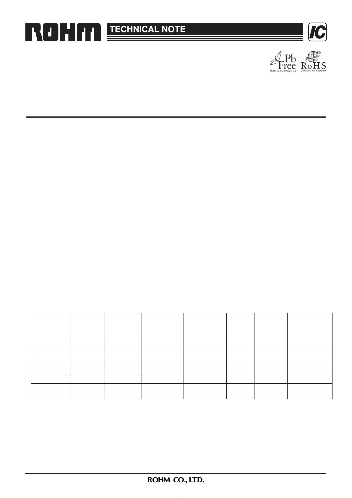
Supply
Product name
BU52001GUL 2.40㨪3.30 +/-3.7 0.8 50 8.0㱘 CMOS VCSP50L1
BU52015GUL 1.65㨪3.30 +/-3.0 0.9 50 5.0㱘 CMOS VCSP50L1
BU52051NVX 1.65㨪3.30 +/-3.0 0.9 50 5.0㱘 CMOS SSON004X1216
BU52011HFV 1.65㨪3.30 +/-3.0 0.9 50 5.0㱘 CMOS HVSOF5
BU52021HFV 2.40㨪3.60 +/-3.7 0.8 50 8.0㱘 CMOS HVSOF5
BU52025G 2.40㨪3.60 +/-3.7 0.8 50 8.0㱘 CMOS SSOP5
BD7411G 4.50㨪5.50 +/-3.4 0.4 - 2.0m CMOS SSOP5
㶎Plus is expressed on the S-pole; minus on the N-pole
voltage
(V)
Operate
point
(mT)
Hysteresis
(mT)
Period
(ms)
Supply
current
(AVG)
(A)
Output
type
Package
Jul. 2008

٨Absolute Maximum Ratings
BU52001GUL (Ta=25㷄) BU52015GUL (Ta=25㷄)
PARAMETERS SYMBOL LIMIT UNIT PARAMETERS SYMBOL LIMIT UNIT
1
Power Supply Voltage
Output Current
V
I
OUT
Power Dissipation Pd
Operating Temperature Range T
Storage Temperature Range T
DD
opr
stg
-0.1㨪+4.5
r1
2
420
-40㨪+85
-40㨪+125
㶎1. Not to exceed Pd
㶎2. Reduced by 4.20mW for each increase in Ta of 1㷄 over 25㷄
䋨mounted on 50mm㬍58mm Glass-epoxy PCB䋩
V
mA
mW
Power Supply Voltage
Output Current
Power Dissipation Pd
Operating Temperature Range T
Storage Temperature Range T
㶎3. Not to exceed Pd
㶎4. Reduced by 4.20mW for each increase in Ta of 1㷄 over 25㷄
䋨mounted on 50mm㬍58mm Glass-epoxy PCB䋩
BU52051NVX (Ta=25㷄) BU52011HFV (Ta=25㷄)
PARAMETERS SYMBOL LIMIT UNIT PARAMETERS SYMBOL LIMIT UNIT
5
Power Supply Voltage
Output Current
V
I
OUT
Power Dissipation Pd
Operating Temperature Range T
Storage Temperature Range T
DD
-0.1㨪+4.5
r0.5
6
2049
opr
stg
-40㨪+85
-40㨪+125
V
mA
mW
Power Supply Voltage
Output Current
Power Dissipation Pd
Operating Temperature Range T
Storage Temperature Range T
㶎5. Not to exceed Pd
㶎6. Reduced by 20.49mW for each increase in Ta of 1㷄 over 25㷄
䋨mounted on 70mm㬍70 mm㬍1.6mm Glass-epoxy PCB䋩
㶎7. Not to exceed Pd
㶎8. Reduced by 5.36mW for each increase in Ta of 1㷄 over 25㷄
䋨mounted on 70mm㬍70 mm㬍1.6mm Glass-epoxy PCB䋩
BU52021NVX (Ta=25㷄) BU52025G (Ta=25㷄)
PARAMETERS SYMBOL LIMIT UNIT PARAMETERS SYMBOL LIMIT UNIT
9
Power Supply Voltage
V
DD
-0.1㨪+4.5
V
Power Supply Voltage
V
I
V
I
V
OUT
OUT
3
DD
-0.1㨪+4.5
r0.5
4
420
opr
stg
DD
-40㨪+85
-40㨪+125
-0.1㨪+4.5
r0.5
8
536
opr
stg
-40㨪+85
-40㨪+125
-0.1㨪+4.5
DD
11
V
mA
mW
7
V
mA
mW
V
I
Output Current
OUT
Power Dissipation Pd
Operating Temperature Range T
Storage Temperature Range T
opr
stg
r1
10
536
-40㨪+85
-40㨪+125
㶎9. Not to exceed Pd
㶎10. Reduced by5.36mW for each increase in Ta of 1㷄 over 25㷄
䋨mounted on 70mm㬍70 mm㬍1.6mm Glass-epoxy PCB䋩
mA
mW
Output Current
Power Dissipation Pd
Operating Temperature Range T
Storage Temperature Range T
㶎11. Not to exceed Pd
㶎12. Reduced by 5.40mW for each increase in Ta of 1㷄 over 25㷄
䋨mounted on 70mm㬍70 mm㬍1.6mm Glass-epoxy PCB䋩
BD7411G (Ta=25㷄)
PARAMETERS SYMBOL LIMIT UNIT
13
Power Supply Voltage
Output Current
V
I
OUT
Power Dissipation Pd
Operating Temperature Range T
Storage Temperature Range T
DD
opr
stg
-0.3㨪+7.0
-55㨪+150
r1
14
540
-40㨪+85
㶎13. Not to exceed Pd
㶎14. Reduced by 5.40mW for each increase in Ta of 1㷄 over 25㷄
䋨mounted on 70mm㬍70 mm
㬍1.6mm Glass-epoxy PCB䋩
V
mA
mW
I
OUT
r1
12
540
opr
stg
-40㨪+85
-40㨪+125
mA
mW
2/20

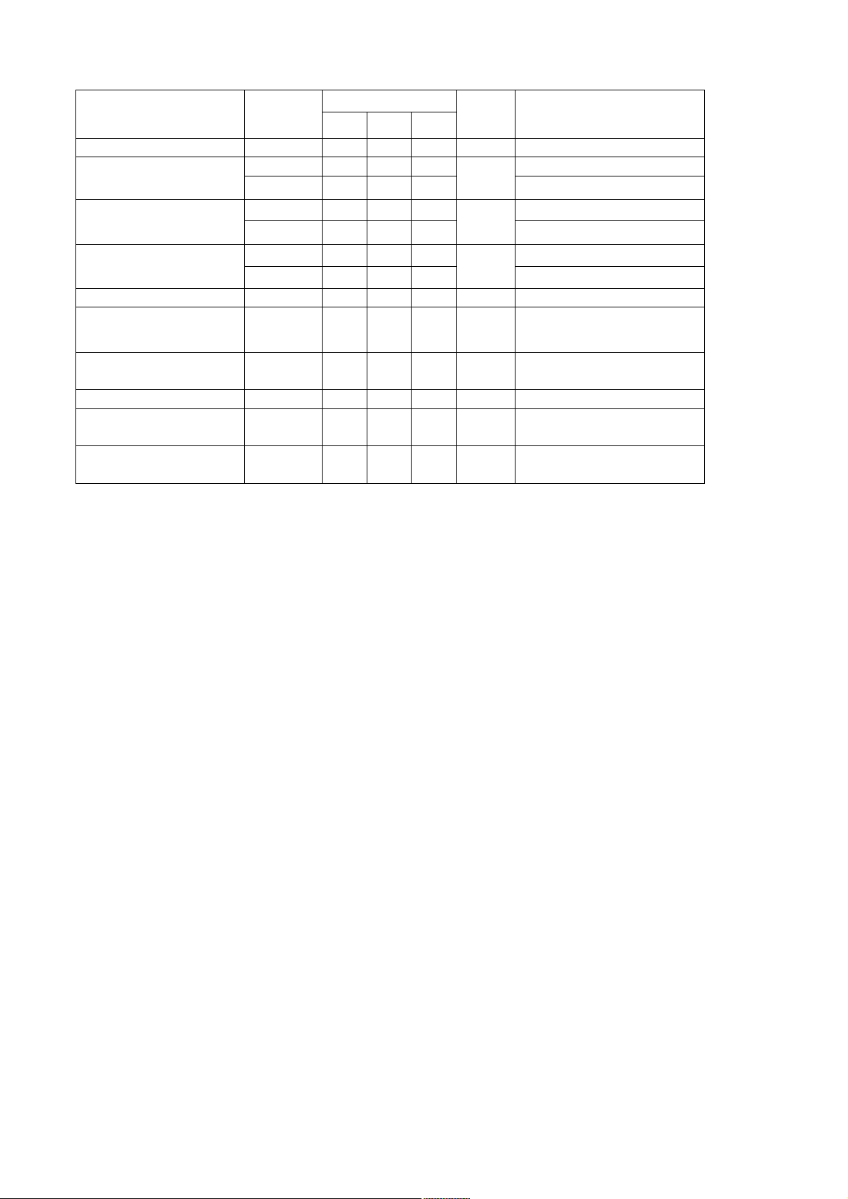
٨Magnetic, Electrical Characteristics
BU52001GUL (Unless otherwise specified, V
PARAMETERS SYMBOL
Power Supply Voltage
Operate Point
Release Point
Hysteresis
2.4 3.0 3.3 V
V
DD
B
- 3.7 5.5
opS
B
opN
0.8 2.9 -
B
rpS
B
rpN
B
hysS
B
hysN
䋽3.0V, Ta䋽25㷄) 㩷㩷㩷㩷 㩷㩷㩷㩷㩷
DD
LIMIT
MIN TYP MAX
-5.5 -3.7 -
- -2.9 -0.8
- 0.8 -
- 0.8 -
UNIT CONDITIONS
mT
mT
mT
Period Tp - 50 100 ms
V
Output High Vol䌴age V
OH
DD
-0.4
- - V
Output Low Voltage VOL - - 0.4 V
Supply Current I
Supply Current
During Startup Time
Supply Current
During Standby Time
- 8 12 ǴA Average
DD(AVG)
I
- 4.7 - mA During Startup Time Value
DD(EN)
- 3.8 - 㱘A During Standby Time Value
I
DD(DIS)
B
<B<B
rpN
=-1.0mA
I
OUT
B<B
opN,BopS
=+1.0mA
I
OUT
15
rpS
<B 15
㶎15 B = Magnetic flux density 㩷㩷㩷㩷㩷㩷㩷㩷㩷㩷㩷㩷㩷㩷㩷㩷㩷㩷㩷㩷㩷㩷㩷㩷㩷㩷㩷㩷㩷㩷㩷㩷㩷㩷㩷㩷㩷㩷
1mT=10Gauss
Positive (“+”) polarity flux is defined as the magnetic flux from south pole which is direct toward to
the branded face of the sensor.
After applying power supply, it takes one cycle of period (T
) to become definite output.
P
Radiation hardiness is not designed.
3/20

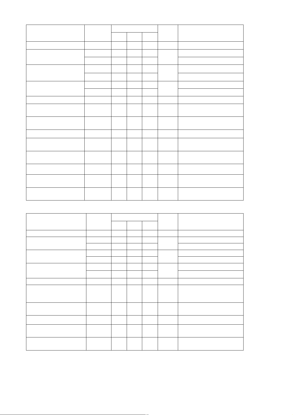
BU52015GUL (Unless otherwise specified,
PARAMETERS SYMBOL
㪭㪛㪛䋽㪈㪅㪏㪇㪭㪃㩷㪫㪸䋽㪉㪌㷄㪀
LIMIT
MIN TYP MAX
UNIT CONDITIONS
Power Supply Voltage VDD 1.65 1.80 3.30 V
B
- 3.0 5.0
Operate Point
Release Point
opS
mT
B
-5.0 -3.0 -
opN
B
0.6 2.1 -
rpS
mT
B
- -2.1 -0.6
rpN
Hysteresis
B
hysS
B
hysN
- 0.9 mT
- 0.9 -
Period Tp - 50 100 ms
OUT1: B
OUT2: B<B
I
Output High Vol䌴age V
OH
V
DD
-0.2
- - V
OUT1: B<B
Output Low Voltage VOL - - 0.2 V
OUT2: B
I
Supply Current 1 I
Supply Current
During Startup Time 1
Supply Current
During Standby Time 1
Supply Current 2 I
Supply Current
During Startup Time 2
Supply Current
During Standby Time 2
DD1(AVG)
I
DD1(EN)
I
DD1(DIS)
DD2(AVG)
I
DD2(EN)
I
DD2(DIS)
- 5 8 㱘A VDD=1.8V, Average
- 2.8 - mA
- 1.8 - 㱘A
VDD=1.8V,
During Startup Time Value
VDD=1.8V,
During Standby Time Value
- 8 12 㱘A VDD=2.7V, Average
- 4.5 - mA
- 4.0 - 㱘A
VDD=2.7V,
During Startup Time Value
V
During Standby Time Value
OUT
OUT
DD
=2.7V,
<B<B
rpN
opN
= -0.5mA
opN
<B<B
rpN
= +0.5mA
, B
, B
rpS
opS
opS
rpS
㶎16 B = Magnetic flux density 㩷㩷㩷㩷㩷㩷㩷㩷㩷㩷㩷㩷㩷㩷㩷㩷㩷㩷㩷㩷㩷㩷㩷㩷㩷㩷㩷㩷㩷㩷㩷㩷㩷㩷㩷㩷㩷㩷
1mT=10Gauss
Positive (“+”) polarity flux is defined as the magnetic flux from south pole which is direct toward to
the branded face of the sensor.
After applying power supply, it takes one cycle of period (T
) to become definite output.
P
Radiation hardiness is not designed.
16
㩷㩷㩷 㩷
<B
<B 16
4/20

BU52051NVX , BU52011HFV (Unless otherwise specified, V
LIMIT
PARAMETERS SYMBOL
MIN TYP MAX
䋽1.80V, Ta䋽25㷄)㩷㩷
DD
UNIT CONDITIONS
Power Supply Voltage VDD 1.65 1.80 3.30 V
Operate Point
Release Point
Hysteresis
opS
B
-5.0 -3.0 -
opN
B
0.6 2.1 -
rpS
B
- -2.1 -0.6
rpN
- 0.9 -
B
hysS
B
- 0.9 -
hysN
mT
mT
mT
- 3.0 5.0
B
Period Tp - 50 100 ms
Output High Vol䌴age V
OH
DD
-0.2
- - V
V
Output Low Voltage VOL - - 0.2 V
Supply Current 1 I
Supply Current
During Startup Time 1
Supply Current
During Standby Time 1
Supply Current 2 I
Supply Current
During Startup Time 2
Supply Current
During Standby Time 2
DD1(AVG)
I
DD1(EN)
I
DD1(DIS)
DD2(AVG)
I
DD2(EN)
I
DD2(DIS)
- 5 8 㱘A VDD=1.8V, Average
-
-
-
-
2.8
1.8
-
8
4.5
4.0
- mA
- 㱘A
12 㱘A VDD=2.7V, Average
- mA
- 㱘A
B
<B<B
rpN
=-0.5mA
I
OUT
B<B
opN
=+0.5mA
I
OUT
V
=1.8V,
DD
17
rpS
, B
<B17
opS
During Startup Time Value
VDD=1.8V,
During Standby Time Value
VDD=2.7V,
During Startup Time Value
V
=2.7V,
DD
During Standby Time Value
BU52021HFV,BU52025G (Unless otherwise specified, VDD䋽3.0V, Ta䋽25㷄) 㩷㩷㩷㩷㩷㩷㩷㩷㩷㩷㩷
PARAMETERS SYMBOL
MIN TYP MAX
LIMIT
UNIT CONDITIONS
Power Supply Voltage VDD 2.4 3.0 3.6 V
B
- 3.7 5.5
Operate Point
Release Point
Hysteresis
opS
B
-5.5 -3.7 -
opN
B
0.8 2.9 -
rpS
B
- -2.9 -0.8
rpN
B
hysS
B
hysN
- 0.8 -
- 0.8 -
mT
mT
mT
Period Tp - 50 100 ms
Output High Vol䌴age V
OH
DD
-0.4
- - V
V
Output Low Voltage VOL - - 0.4 V
I
Supply Current
Supply Current
During Startup Time
Supply Current
During Standby Time
DD(AVG)
I
-
DD(EN)
I
-
DD(DIS)
-
8
4.7
3.8
12 ǴA Average
- mA During Startup Time Value
- 㱘A During Standby Time Value
B
<B<B
rpN
=-1.0mA
I
OUT
B<B
opN
=+1.0mA
I
OUT
17
rpS
, B
<B 17
opS
㶎17 B = Magnetic flux density 㩷㩷㩷㩷㩷㩷㩷㩷㩷㩷㩷㩷㩷㩷㩷㩷㩷㩷㩷㩷㩷㩷㩷㩷㩷㩷㩷㩷㩷㩷㩷㩷㩷㩷㩷㩷㩷㩷
1mT=10Gauss
Positive (“+”) polarity flux is defined as the magnetic flux from south pole which is direct toward to
the branded face of the sensor.
After applying power supply, it takes one cycle of period (T
) to become definite output.
P
Radiation hardiness is not designed.
5/20

BD7411G (Unless otherwise specified, V
PARAMETERS SYMBOL
䋽5.0V, Ta䋽25㷄)
DD
LIMIT
MIN TYP MAX
UNIT CONDITIONS
Power Supply Voltage V
Operate Point
Release Point
B
Hysteresis
B
Output High Vol䌴age V
Output Low Voltage V
Supply Current I
B
B
B
B
DD
opS
opN
rpS
rpN
hysS
hysN
OH
OL
DD
4.5 5.0 5.5
- 3.4 5.6
-5.6 -3.4 -
1.5 3.0 -
- -3.0 -1.5
- 0.4 -
- 0.4 -
4.6
- -
- - 0.4
- 2 4
V
mT
mT
mT
B
V
V
rpN
I
OUT
B<B
I
OUT
mA
<B<B
rpS
=-1.0mA
, B
opN
opS
=+1.0mA
18
<B 18
㶎18 B = Magnetic flux density 㩷㩷㩷㩷㩷㩷㩷㩷㩷㩷㩷㩷㩷㩷㩷㩷㩷㩷㩷㩷㩷㩷㩷㩷㩷㩷㩷㩷㩷㩷㩷㩷㩷㩷㩷㩷㩷㩷
1mT=10Gauss
Positive (“+”) polarity flux is defined as the magnetic flux from south pole which is direct toward to
the branded face of the sensor.
Radiation hardiness is not designed.
6/20
 Loading...