

Hall ICs
Unipolar Detection
Hall ICs
BU52002GUL,BU52003GUL,BU52012NVX,BU52012HFV,BU52013HFV
●Description
The unipolar Detection Hall IC detects only either the N pole or S pole.
The output turns ON (active Low) upon detection.
●Features
1) Unipolar detection
2) Micropower operation (small current using intermittent operation method)
3) Ultra-compact CSP4 package (BU52002GUL, BU52003GUL)
4) Ultra- Small outline package (BU52012NVX)
5) Small outline package (BU52012HFV, BU52013HFV)
6) Line up of supply voltage
For 1.8V Power supply voltage (BU52012NVX, BU52012HFV, BU52013HFV)
For 3.0V Power supply voltage (BU52002GUL, BU52003GUL)
7) High ESD resistance 8kV(HBM)
●Applications
Mobile phones, notebook computers, digital video camera, digital still camera, etc.
●Lineup matrix
Supply
current
(AVG.)
(µA)
Output type Package
Function Product name
BU52002GUL 2.40~3.30 3.7
Supply
voltage
(V)
Operate
point
(mT)
Hysteresis
(mT)
※
0.8 50 6.5
Period
(ms)
CMOS
No.10045ECT03
VCSP50L1
S pole
N pole
※Plus is expressed on the S-pole; minus on the N-pole
BU52012NVX 1.65~3.60 3.0 ※ 0.9 50 3.5
BU52012HFV 1.65~3.30 3.0 ※ 0.9 50 3.5
BU52003GUL 2.40~3.30 -3.7
BU52013HFV 1.65~3.30 -3.0 ※ 0.9 50 3.5
※
0.8 50 6.5
COMS
CMOS
CMOS
CMOS
SSON004X1216
HVSOF5
VCSP50L1
HVSOF5
www.rohm.com
© 2010 ROHM Co., Ltd. All rights reserved.
1/19
2010.08 - Rev.C

BU52002GUL,BU52003GUL,BU52012NVX,BU52012HFV,BU52013HFV
●Absolute maximum ratings
BU52002GUL,BU52003GUL (Ta=25℃) BU52012NVX (Ta=25℃)
Parameter Symbol Ratings Unit Parameter Symbol Ratings Unit
1
Power Supply Voltage VDD -0.1~+4.5
※
V Power Supply Voltage VDD -0.1~+4.5
Technical Note
3
※
V
Output Current I
OUT
Power Dissipation Pd 420
Operating
Temperature Range
Storage
Temperature Range
※1. Not to exceed Pd
※2. Reduced by 4.20mW for each increase in Ta of 1℃ over 25℃
(mounted on 50mm×58mm Glass-epoxy PCB)
T
-40~+85 ℃
opr
-40~+125 ℃
T
stg
±1 mA Output Current I
2
※
mW Power Dissipation Pd 2049
BU52012HFV,BU52013HFV (Ta=25℃)
Parameter Symbol Ratings Unit
5
±0.5
536
※
6
※
Power Supply Voltage VDD
Output Current I
OUT
-0.1~+4.5
Power Dissipation Pd
Operating
Temperature Range
Storage
Temperature Range
※5. Not to exceed Pd
※6. Reduced by 5.36mW for each increase in Ta of 1℃ over 25℃
(mounted on 70mm×70mm×1.6mm Glass-epoxy PCB)
T
-40~+85
-40~+125
opr
T
stg
●Magnetic, Electrical characteristics
BU52002GUL (Unless otherwise specified, VDD=3.0V, Ta=25℃)
Parameter Symbol
Min. Typ. Max.
Operating
Temperature Range
Storage
Temperature Range
※3. Not to exceed Pd
※4. Reduced by 5.36mW for each increase in Ta of 1℃ over 25℃
(mounted on 70mm×70mm×1.6mm Glass-epoxy PCB)
V
mA
mW
℃
℃
Limits
OUT
T
-40~+85 ℃
opr
-40~+125 ℃
T
stg
±0.5 mA
※4
mW
Unit Conditions
Power Supply Voltage VDD 2.4 3.0 3.3 V
Operate Point B
Release Point B
Hysteresis B
- 3.7 5.5 mT
opS
0.8 2.9 - mT
rpS
- 0.8 - mT
hysS
Period TP - 50 100 ms
B<B
Output High Voltage VOH VDD-0.4 - - V
Output Low Voltage VOL - - 0.4 V
Supply Current I
Supply Current
During Startup Time
Supply Current
During Standby Time
※7. B = Magnetic flux density
1mT=10Gauss
Positive (“+”) polarity flux is defined as the magnetic flux from south pole which is direct toward to the branded face of the sensor.
After applying power supply, it takes one cycle of period (T
Radiation hardiness is not designed.
- 6.5 9 µA Average
DD(AVG)
I
- 4.7 - mA During Startup Time Value
DD(EN)
- 3.8 - µA During Standby Time Value
I
DD(DIS)
) to become definite output.
P
rpS
I
=-1.0mA
OUT
<B
B
opS
I
=+1.0mA
OUT
7
※
7
※
www.rohm.com
© 2010 ROHM Co., Ltd. All rights reserved.
2/19
2010.08 - Rev.C

BU52002GUL,BU52003GUL,BU52012NVX,BU52012HFV,BU52013HFV
BU52003GUL (Unless otherwise specified, VDD=3.0V, Ta=25℃)
Parameter Symbol
Min. Typ. Max.
Limits
Unit Conditions
Power Supply Voltage VDD 2.4 3.0 3.3 V
Technical Note
Operate Point B
Release Point B
Hysteresis B
-5.5 -3.7 - mT
opN
- -2.9 -0.8 mT
rpN
- 0.8 - mT
hysN
Period TP - 50 100 ms
<B
B
Output High Voltage VOH VDD-0.4 - - V
Output Low Voltage VOL - - 0.4 V
Supply Current I
Supply Current
During Startup Time
Supply Current
During Standby Time
※8. B = Magnetic flux density
1mT=10Gauss
Positive (“+”) polarity flux is defined as the magnetic flux from south pole which is direct toward to the branded face of the sensor.
After applying power supply, it takes one cycle of period (T
Radiation hardiness is not designed.
- 6.5 9 µA Average
DD(AVG)
- 4.7 - mA During Startup Time Value
I
DD(EN)
- 3.8 - µA During Standby Time Value
I
DD(DIS)
) to become definite output.
P
rpN
I
=-1.0mA
OUT
B<B
opN
I
=+1.0mA
OUT
8
※
8
※
www.rohm.com
© 2010 ROHM Co., Ltd. All rights reserved.
3/19
2010.08 - Rev.C

BU52002GUL,BU52003GUL,BU52012NVX,BU52012HFV,BU52013HFV
BU52012NVX (Unless otherwise specified, VDD=1.80V, Ta=25℃)
Parameter Symbol
Min. Typ. Max.
Limits
Unit Conditions
Power Supply Voltage VDD 1.65 1.80 3.60 V
Technical Note
Operate Point B
Release Point B
Hysteresis B
- 3.0 5.0 mT
opS
0.6 2.1 - mT
rpS
- 0.9 - mT
hysS
Period TP - 50 100 ms
B<B
Output High Voltage VOH VDD-0.2 - - V
Output Low Voltage VOL - - 0.2 V
Supply Current 1 I
Supply Current
During Startup Time 1
Supply Current
During Standby Time 1
Supply Current 2 I
Supply Current
During Startup Time 2
Supply Current
During Standby Time 2
※9. B = Magnetic flux density
1mT=10Gauss
Positive (“+”) polarity flux is defined as the magnetic flux from south pole which is direct toward to the branded face of the sensor.
After applying power supply, it takes one cycle of period (T
Radiation hardiness is not designed.
- 3.5 5.5 µA VDD=1.8V, Average
DD1(AVG)
- 2.8 - mA
I
DD1(EN)
- 1.8 - µA
I
DD1(DIS)
- 8.0 12.5 µA VDD=3.0V, Average
DD2(AVG)
I
- 5.3 - mA
DD2(EN)
I
- 5.2 - µA
DD2(DIS)
) to become definite output.
P
rpS
I
=-0.5mA
OUT
B
<B
opS
I
=+0.5mA
OUT
=1.8V,
V
DD
During Startup Time Value
=1.8V,
V
DD
During Standby Time Value
=3.0V,
V
DD
During Startup Time Value
VDD=3.0V,
During Standby Time Value
9
※
9
※
www.rohm.com
© 2010 ROHM Co., Ltd. All rights reserved.
4/19
2010.08 - Rev.C

BU52002GUL,BU52003GUL,BU52012NVX,BU52012HFV,BU52013HFV
BU52012HFV (Unless otherwise specified, VDD=1.80V, Ta=25℃)
Parameter Symbol
Min. Typ. Max.
Limits
Unit Conditions
Power Supply Voltage VDD 1.65 1.80 3.30 V
Technical Note
Operate Point B
Release Point B
Hysteresis B
- 3.0 5.0 mT
opS
0.6 2.1 - mT
rpS
- 0.9 - mT
hysS
Period TP - 50 100 ms
B<B
Output High Voltage VOH VDD-0.2 - - V
Output Low Voltage VOL - - 0.2 V
Supply Current 1 I
Supply Current
During Startup Time 1
Supply Current
During Standby Time 1
Supply Current 2 I
Supply Current
During Startup Time 2
Supply Current
During Standby Time 2
※10. B = Magnetic flux density
1mT=10Gauss
Positive (“+”) polarity flux is defined as the magnetic flux from south pole which is direct toward to the branded face of the sensor.
After applying power supply, it takes one cycle of period (T
Radiation hardiness is not designed.
- 3.5 5.5 µA VDD=1.8V, Average
DD1(AVG)
- 2.8 - mA
I
DD1(EN)
- 1.8 - µA
I
DD1(DIS)
- 6.5 9 µA VDD=2.7V, Average
DD2(AVG)
I
- 4.5 - mA
DD2(EN)
I
- 4.0 - µA
DD2(DIS)
) to become definite output.
P
rpS
I
=-0.5mA
OUT
B
<B
opS
I
=+0.5mA
OUT
=1.8V,
V
DD
During Startup Time Value
=1.8V,
V
DD
During Standby Time Value
=2.7V,
V
DD
During Startup Time Value
VDD=2.7V,
During Standby Time Value
10
※
10
※
www.rohm.com
© 2010 ROHM Co., Ltd. All rights reserved.
5/19
2010.08 - Rev.C

BU52002GUL,BU52003GUL,BU52012NVX,BU52012HFV,BU52013HFV
BU52013HFV (Unless otherwise specified, VDD=1.80V, Ta=25℃)
Parameter Symbol
Min. Typ. Max.
Limits
Unit Conditions
Power Supply Voltage VDD 1.65 1.80 3.30 V
Technical Note
Operate Point B
Release Point B
Hysteresis B
-5.0 -3.0 - mT
opN
- -2.1 -0.6 mT
rpN
- 0.9 - mT
hysN
Period TP - 50 100 ms
Output High Voltage VOH
DD
-0.2
- - V
V
Output Low Voltage VOL - - 0.2 V
Supply Current 1 I
Supply Current
During Startup Time 1
Supply Current
During Standby Time 1
Supply Current 2 I
Supply Current
During Startup Time 2
Supply Current
During Standby Time 2
※11. B = Magnetic flux density
1mT=10Gauss
Positive (“+”) polarity flux is defined as the magnetic flux from south pole which is direct toward to the branded face of the sensor.
After applying power supply, it takes one cycle of period (T
Radiation hardiness is not designed.
- 3.5 5.5 µA VDD=1.8V, Average
DD1(AVG)
- 2.8 - mA
I
DD1(EN)
- 1.8 - µA
I
DD1(DIS)
- 6.5 9 µA VDD=2.7V, Average
DD2(AVG)
I
- 4.5 - mA
DD2(EN)
I
- 4.0 - µA
DD2(DIS)
) to become definite output.
P
B
<B
rpN
I
=-0.5mA
OUT
B<B
opN
I
=+0.5mA
OUT
=1.8V,
V
DD
During Startup Time Value
=1.8V,
V
DD
During Standby Time Value
=2.7V,
V
DD
During Startup Time Value
VDD=2.7V,
During Standby Time Value
11
※
11
※
www.rohm.com
© 2010 ROHM Co., Ltd. All rights reserved.
6/19
2010.08 - Rev.C

BU52002GUL,BU52003GUL,BU52012NVX,BU52012HFV,BU52013HFV
●Figure of measurement circuit
B
op/Brp
Tp
200Ω
VDD
100µF
VDD
GND
OUT
VDD
Oscilloscope
V
Bop and Brp are measured with applying the magnetic field
from the outside.
Fig.1 Bop,Brp measurement circuit
The period is monitored by Oscilloscope.
Fig.2 Tp measurement circuit
OH
V
Product Name I
VDD
100µF
VDD
GND
OUT
BU52002GUL, BU52003GUL 1.0mA
I
OUT
V
BU52012NVX, BU52012HFV,
BU52013HFV
Fig.3 V
measurement circuit
OH
V
OL
Product Name I
VDD
100µF
VDD
GND
OUT
BU52002GUL, BU52003GUL 1.0mA
I
V
OUT
BU52012NVX, BU52012HFV,
BU52013HFV
Fig.4 VOL measurement circuit
IDD
VDD
A
2200µF
VDD
OUT
GND
Fig.5 IDD measurement circuit
Technical Note
VDD
OUT
GND
OUT
0.5mA
OUT
0.5mA
www.rohm.com
© 2010 ROHM Co., Ltd. All rights reserved.
7/19
2010.08 - Rev.C

BU52002GUL,BU52003GUL,BU52012NVX,BU52012HFV,BU52013HFV
●Technical (Reference) Data
BU52002GUL (VDD=2.4~3.3V type)
8.0
V
=3.0V
DD
6.0
4.0
2.0
0.0
-2.0
-4.0
-6.0
MAGNETIC FLUX DENSITY [mT]
-8.0
-60 -40 - 20 0 20 40 60 80 100
AMBIENT TEM PERATU RE [℃]
Bop S
Brp S
Fig.6 Bop,Brp – Ambient temperature
8.0
Ta = 25°C
6.0
4.0
2.0
0.0
-2.0
-4.0
-6.0
MAGNETIC FLUX DENSITY [mT]
-8.0
2.0 2.4 2.8 3.2 3.6
SUPPLY VOLTAGE [V
Bop S
Brp S
]
Fig.7 Bop,Brp – Supply voltage
100
90
80
70
60
50
40
PERIOD [ms]
30
20
10
0
-60 -40 - 20 0 20 40 60 80 100
Fig.8 T
100
90
Ta = 25°C
80
70
60
50
40
30
PERIOD [ms]
20
10
0
2.0 2.4 2. 8 3.2 3.6
SUPPLY VOLTAGE [V]
Fig.9 T
– Supply voltage
P
20.0
18.0
VDD=3.0V
16.0
14.0
12.0
10.0
8.0
6.0
4.0
2.0
0.0
AVERAGE SUPPLY CURRENT [µA]
-60 -40 -20 0 20 40 60 80 100
AMBIEN T TEMPER ATURE [℃]
Fig.10 IDD – Ambient temperature
20.0
18.0
16.0
14.0
12.0
10.0
8.0
6.0
4.0
2.0
0.0
AVERAGE SUPPLY CURRENT [µA]
Fig.11 I
BU52003GUL (VDD=2.4~3.3V type)
8.0
6.0
VDD=3.0V
4.0
2.0
0.0
-2.0
-4.0
-6.0
MAGNETIC FLUX DENSITY [mT]
-8.0
-60 -40 - 20 0 20 40 60 80 100
AMBIENT TEM PERATU RE [℃]
Brp N
Bop N
Fig.12 Bop,Brp – Ambient temperature
8.0
Ta = 25°C
6.0
4.0
2.0
0.0
-2.0
-4.0
-6.0
MAGNETIC FLUX DENSITY [mT]
-8.0
2.0 2. 4 2.8 3.2 3.6
SUPPLY VOLT AGE [V
Brp N
Bop N
]
Fig.13 Bop,Brp – Supply voltage
100
90
80
70
60
50
40
PERIOD [ms]
30
20
10
Fig.14 T
100
Ta = 25°C
90
80
70
60
50
40
PERIOD [ms]
30
20
10
0
2.0 2.4 2.8 3.2 3.6
SUPPLY VOLTAGE [ V]
Fig.15 T
–Supply voltage
P
20.0
18.0
VDD=3.0V
16.0
14.0
12.0
10.0
8.0
6.0
4.0
2.0
0.0
AVERAGE SUPPLY CURRENT [µA]
-60 -40 -20 0 20 40 60 80 100
AMBIEN T TEMPERAT UR E [℃]
Fig.16 I
– Ambient temperature Fig.17 IDD – Supply voltage
DD
20.0
18.0
16.0
14.0
12.0
10.0
8.0
6.0
4.0
2.0
0.0
AVERAGE SUPPLY CURRENT [µA]
Technical Note
VDD=3.0V
AMBIEN T TEMPER ATURE [℃]
–Ambient temperature
P
Ta = 25°C
2.0 2.4 2.8 3.2 3. 6
SUPPLY VOLTAGE [V]
– Supply voltage
DD
VDD=3.0V
0
-60 - 40 -20 0 20 40 60 80 100
AMBIEN T TEMPER ATURE [℃]
– Ambient temperature
P
Ta = 25°C
2.0 2.4 2. 8 3.2 3.6
SUPPLY VOLTAGE [V]
www.rohm.com
© 2010 ROHM Co., Ltd. All rights reserved.
8/19
2010.08 - Rev.C

BU52002GUL,BU52003GUL,BU52012NVX,BU52012HFV,BU52013HFV
BU52012NVX (VDD=1.65~3.6V type)
8.0
VDD=1.8V
6.0
4.0
2.0
0.0
-2.0
-4.0
-6.0
MAGNETIC FLUX DENSITY [mT]
-8.0
-60 -40 - 20 0 20 40 60 80 100
AMBIEN T TEMPER ATU RE [℃]
Bop S
Brp S
Fig.18 Bop,Brp – Ambient temperature
8.0
Ta = 25°C
6.0
4.0
2.0
0.0
-2.0
-4.0
-6.0
MAGNETIC FLUX DENSITY [mT]
-8.0
1.4 1.8 2. 2 2.6 3.0 3.4 3.8
SUPPLY VOLTAGE [V
Bop S
Brp S
]
Fig.19 Bop,Brp – Supply voltage
100
PERIOD [ms]
Fig.20 TP – Ambient temperature
100
90
Ta = 25°C
80
70
60
50
40
PERIOD [ms]
30
20
10
0
1.41.82.22.63.03.43.8
SUPPLY VOLTAGE [V]
Fig.21 TP – Supply voltage
20.0
18.0
VDD=1.8V
16.0
14.0
12.0
10.0
8.0
6.0
4.0
2.0
0.0
AVERAGE SUPPLY CURRENT [µA]
-60 -40 -20 0 20 40 60 80 100
AMBIEN T TEMPER ATURE [℃]
Fig.22 I
– Ambient temperature
DD
AVERAGE SUPPLY CURRENT [µA]
BU52012HFV (V
DD=1.65~3.3V type)
8.0
VDD=1.8V
6.0
4.0
2.0
0.0
-2.0
-4.0
-6.0
MAGNETIC FLUX DENSITY [mT]
-8.0
-60 - 40 -20 0 20 40 60 80 100
AMBIEN T TEMPER ATU RE [℃]
Bop S
Brp S
Fig.24 Bop,Brp – Ambient temperature
8.0
Ta = 25°C
6.0
4.0
2.0
0.0
-2.0
-4.0
-6.0
MAGNETIC FLUX DENSITY [mT]
-8.0
1.4 1.8 2. 2 2.6 3.0 3.4 3.8
SUPPLY VOLTAGE [V
Bop S
Brp S
]
Fig.25 Bop,Brp – Supply voltage
100
90
80
70
60
50
40
PERIOD [ms]
30
20
10
Fig.26 T
100
90
Ta = 25°C
80
70
60
50
40
PERIOD [ms]
30
20
10
0
1.4 1.8 2.2 2.6 3.0 3.4 3.8
SUPPLY VOLTAGE [V]
Fig.27 TP – Supply voltage
20.0
18.0
VDD=1.8V
16.0
14.0
12.0
10.0
8.0
6.0
4.0
2.0
0.0
AVERAGE SUPPLY CURRENT [µA]
-60 - 40 - 20 0 20 40 60 80 100
AMBIEN T TEMPER ATURE [℃]
Fig.28 IDD – Ambient temperature
20.0
18.0
16.0
14.0
12.0
10.0
8.0
6.0
4.0
2.0
0.0
AVERAGE SUPPLY CURRENT [µA]
Fig.29 I
Technical Note
90
VDD=1.8V
80
70
60
50
40
30
20
10
0
-60 -40 -20 0 20 40 60 80 100
AMBIEN T TEMPER ATUR E [℃]
20.0
18.0
Ta = 25°C
16.0
14.0
12.0
10.0
8.0
6.0
4.0
2.0
0.0
1.4 1.8 2.2 2.6 3.0 3.4 3.8
SUPPLY VOLT AGE [V]
Fig.23 I
VDD=1.8V
0
-60 - 40 - 20 0 20 40 60 80 100
AMBIEN T TEMPER ATUR E [℃]
Ta = 25°C
1.4 1.8 2.2 2.6 3.0 3.4 3.8
– Supply voltage
DD
– Ambient temperature
P
SUPPLY VOLT AGE [V]
– Supply voltage
DD
www.rohm.com
© 2010 ROHM Co., Ltd. All rights reserved.
9/19
2010.08 - Rev.C

BU52002GUL,BU52003GUL,BU52012NVX,BU52012HFV,BU52013HFV
BU52013HFV (VDD=1.65~3.3V type)
8.0
VDD=1.8V
6.0
4.0
2.0
0.0
-2.0
-4.0
-6.0
MAGNETIC FLUX DENSITY [mT]
-8.0
-60 - 40 -20 0 20 40 60 80 100
AMBIEN T TEMPER ATU RE [℃]
Brp N
Bop N
Fig.30 Bop,Brp – Ambient temperature
8.0
Ta = 25°C
6.0
4.0
2.0
0.0
-2.0
-4.0
-6.0
MAGNETIC FLUX DENSITY [mT]
-8.0
1.4 1.8 2. 2 2.6 3.0 3.4 3.8
SUPPLY VOLTAGE [V
Brp N
Bop N
]
Fig.31 Bop,Brp – Supply voltage
100
90
80
70
60
50
40
PERIOD [ms]
30
20
10
0
Fig.32 T
100
90
Ta = 25°C
80
70
60
50
40
PERIOD [ms]
30
20
10
0
1.41.82.22.63.03.43.8
SUPPLY VOLTAGE [ V]
Fig.33 T
– Supply voltage
P
20.0
18.0
VDD=1.8V
16.0
14.0
12.0
10.0
8.0
6.0
4.0
2.0
AVERAGE SUPPLY CURRENT [µA]
0.0
-60 - 40 - 20 0 20 40 60 80 100
AMBIEN T TEMPER ATUR E [℃]
Fig.34 IDD – Ambient temperature
20.0
18.0
16.0
14.0
12.0
10.0
8.0
6.0
4.0
2.0
0.0
AVERAGE SUPPLY CURRENT [µA]
Fig.35 I
Technical Note
VDD=1.8V
-60 - 40 -20 0 20 40 60 80 100
AMBIEN T TEMPER ATURE [℃]
– Ambient temperature
P
Ta = 25°C
1.4 1.8 2. 2 2.6 3.0 3.4 3.8
SUPPLY VOLT AGE [V]
– Supply voltage
DD
www.rohm.com
© 2010 ROHM Co., Ltd. All rights reserved.
10/19
2010.08 - Rev.C

BU52002GUL,BU52003GUL,BU52012NVX,BU52012HFV,BU52013HFV
●Block Diagram
BU52002GUL, BU52003GUL
HALL
ELEMENT
×
TIMING LOGIC
OFFSET
DYNAMIC
CANCELLATION
VDD
A1
SAMPLE
& HOLD
Fig.36
The CMOS output terminals enable direct connection to
the PC, with no external pull-up resistor required.
B1
OUT
LATCH
A2
GND
A1
PIN No. PIN NAME FUNCTION COMMENT
A1 VDD POWER SUPPLY
A2 GND GROUND
B1 OUT OUTPUT
B2 N.C. OPEN or Short to GND.
B1
Surface
BU52012NVX
HALL
ELEMENT
×
TIMING LOGIC
OFFSET
DYNAMIC
CANCELLATION
VDD
SAMPLE
& HOLD
4
Fig.37
LATCH
The CMOS output terminals enable direct
connection to the PC, with no external pull-up
resistor required.
OUT
1
2
GND
4 3
PIN No. PIN NAME FUNCTION COMMENT
1 OUT OUTPUT
2 GND GROUND
3 N.C. OPEN or Short to GND.
4 VDD POWER SUPPLY
1 2
Surface
Technical Note
0.1µF
Adjust the bypass capacitor value as
necessary, according to voltage noise
conditions, etc.
A2
A2
B2
0.1µF
Adjust the bypass capacitor value as
necessary, according to voltage
noise conditions, etc.
A1
B2
B1
Reverse
3 4
2 1
Reverse
www.rohm.com
© 2010 ROHM Co., Ltd. All rights reserved.
11/19
2010.08 - Rev.C

BU52002GUL,BU52003GUL,BU52012NVX,BU52012HFV,BU52013HFV
BU52012HFV, BU52013HFV
HALL
ELEMENT
×
TIMING LOGIC
OFFSET
DYNAMIC
CANCELLATION
VDD
SAMPLE
& HOLD
4
The CMOS output terminals enable direct connection to
the PC, with no external pull-up resistor required.
OUT
5
LATCH
2
GND
Fig.38
5
PIN No. PIN NAME FUNCTION COMMENT
1 N.C. OPEN or Short to GND.
2 GND GROUND
3 N.C. OPEN or Short to GND.
4 VDD POWER SUPPLY
5 OUT OUTPUT
1
Surface
●Description of Operations
(Micropower Operation)
I
DD
Startup time
Fig.39
The unipolar detection Hall IC adopts an intermittent operation
method to save energy. At startup, the Hall elements, amp,
comparator and other detection circuit power ON and magnetic
detection begins. During standby, the detection circuits power
OFF, thereby reducing current consumption. The detection results
are held while standby is active, and then output.
Reference period: 50ms (MAX100ms)
Reference startup time: 24µs
t
(Offset Cancelation)
VDD
B
×
GND
I
bridge circuit. Offset voltage may be generated by a differential in
this bridge resistance, or can arise from changes in resistance
due to package or bonding stress. A dynamic offset cancellation
circuit is employed to cancel this offset voltage.
When Hall elements are connected as shown in Fig. 40 and a
The Hall elements form an equivalent Wheatstone (resistor)
+
magnetic field is applied perpendicular to the Hall elements,
voltage is generated at the mid-point terminal of the bridge. This
is known as Hall voltage.
Hall Voltage
Dynamic cancellation switches the wiring (shown in the figure) to
redirect the current flow to a 90˚ angle from its original path, and
-
thereby cancels the Hall voltage.
The magnetic signal (only) is maintained in the sample/hold
circuit during the offset cancellation process and then released.
Fig.40
Technical Note
0.1µF
Adjust the bypass capacitor value as
necessary, according to voltage noise
conditions, etc.
4
2
3
4
3
Reverse
5
2
1
www.rohm.com
© 2010 ROHM Co., Ltd. All rights reserved.
12/19
2010.08 - Rev.C

BU52002GUL,BU52003GUL,BU52012NVX,BU52012HFV,BU52013HFV
(Magnetic Field Detection Mechanism)
The Hall IC cannot detect magnetic fields that run horizontal to the package top layer.
Be certain to configure the Hall IC so that the magnetic field is perpendicular to the top layer.
S
S
S
N
Flux
Fig.41
S
Technical Note
N
N
Flux
www.rohm.com
© 2010 ROHM Co., Ltd. All rights reserved.
13/19
2010.08 - Rev.C

BU52002GUL,BU52003GUL,BU52012NVX,BU52012HFV,BU52013HFV
BU52002GUL,BU52012HFV
S-Pole
S
S
N
OUT [V]
High
BU52002GUL, BU52012HFV detects and outputs for the S-pole only. Since it is unipolar, it does not recognize the N-pole.
BU52003GUL, BU52013HFV
N-Pole
High
Low
Bop N
BU52003GUL, BU52013HFV detects and outputs for the N-pole only. Since it is unipolar, it does not recognize the S-pole.
The unipolar detection Hall IC detects magnetic fields running perpendicular to the top surface of the package. There is an
inverse relationship between magnetic flux density and the distance separating the magnet and the Hall IC: when distance
increases magnetic density falls. When it drops below the operate point (Bop), output goes HIGH. When the magnet gets
closer to the IC and magnetic density rises, to the operate point, the output switches LOW. In LOW output mode, the
distance from the magnet to the IC increases again until the magnetic density falls to a point just below Bop, and output
returns HIGH. (This point, where magnetic flux density restores HIGH output, is known as the release point, Brp.) This
detection and adjustment mechanism is designed to prevent noise, oscillation and other erratic system operation.
Flux
N-Pole
Fig.42 S-Pole Detection
S
S
N
Flux
Brp N
N-Pole
Fig.43 N-Pole Detection
High
0
Magnetic flux density [mT]
OUT [V]
High
0
Magnetic flux density [mT]
N
N
S
Flux
Brp S
S-Pole
N
N
S
Flux
S-Pole
Technical Note
High
Low
Bop S
High
B
B
www.rohm.com
© 2010 ROHM Co., Ltd. All rights reserved.
14/19
2010.08 - Rev.C
BU52002GUL,BU52003GUL,BU52012NVX,BU52012HFV,BU52013HFV
Technical Note
●Intermittent Operation at Power ON
Power ON
VDD
Supply current
(Intermittentaction)
OUT
(No magnetic
field present)
OUT
(Magnetic
field present)
Startup time
Indefinite
interval
Indefinite
interval
Standby time
High
Low
Fig.44
Startup time
Standby time
The unipolar detection Hall IC adopts an intermittent operation method in detecting the magnetic field during startup, as
shown in Fig.44. It outputs to the appropriate terminal based on the detection result and maintains the output condition
during the standby period. The time from power ON until the end of the initial startup period is an indefinite interval, but it
cannot exceed the maximum period, 100ms. To accommodate the system design, the Hall IC output read should be
programmed within 100ms of power ON, but after the time allowed for the period ambient temperature and supply voltage.
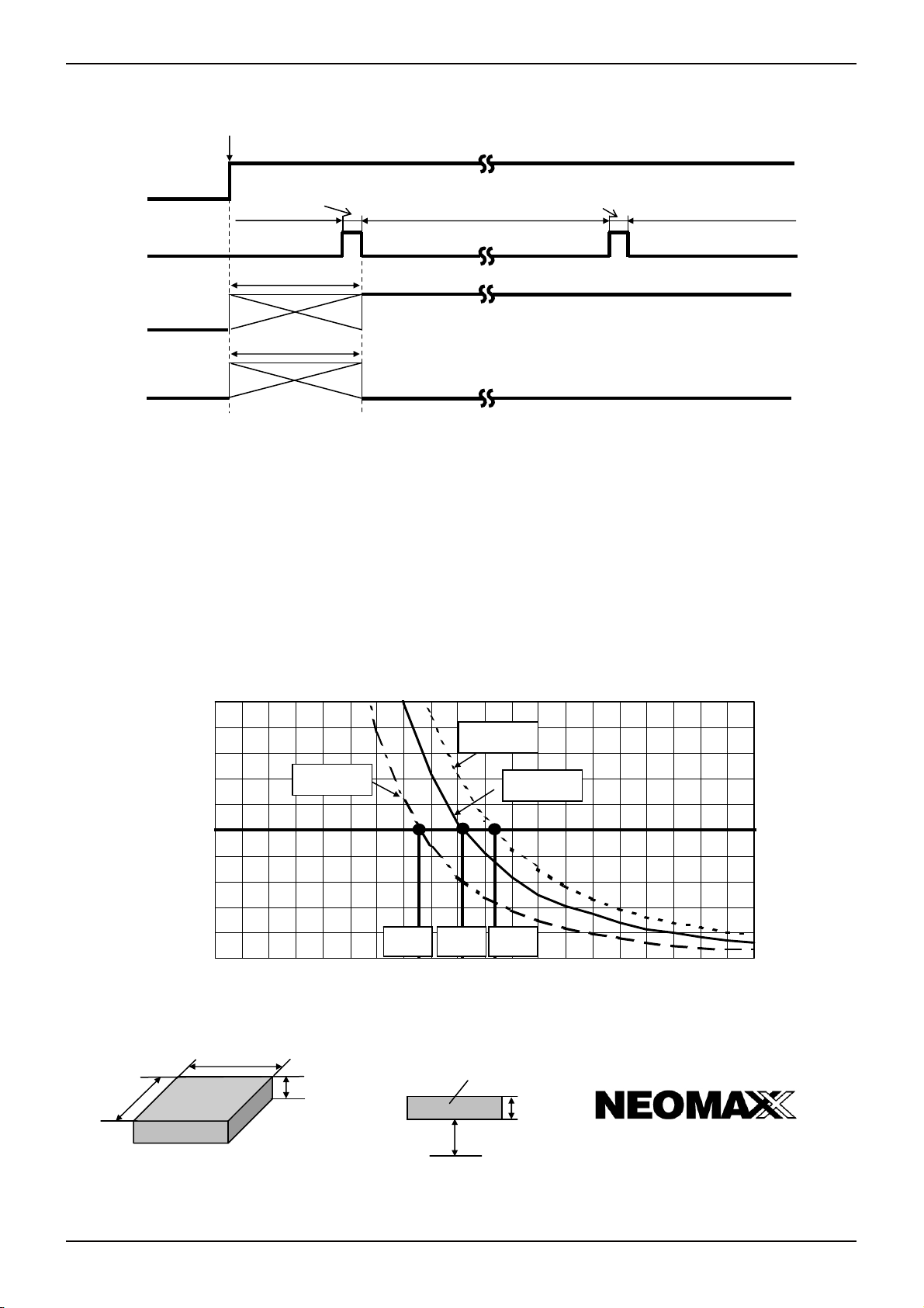
●Magnet Selection
Of the two representative varieties of permanent magnet, neodymium generally offers greater magnetic power per volume
than ferrite, thereby enabling the highest degree of miniaturization, thus, neodymium is best suited for small equipment
applications. Fig.45 shows the relation between the size (volume) of a neodymium magnet and magnetic flux density. The
graph plots the correlation between the distance (L) from three versions of a 4mm X 4mm cross-section neodymium magnet
(1mm, 2mm, and 3mm thick) and magnetic flux density. Fig.46 shows Hall IC detection distance – a good guide for
determining the proper size and detection distance of the magnet. Based on the BU52012HFV, BU52013HFV operating
point max 5.0 mT, the minimum detection distance for the 1mm, 2mm and 3mm magnets would be 7.6mm, 9.22mm, and
10.4mm, respectively. To increase the magnet’s detection distance, either increase its thickness or sectional area.
10
9
8
7
t=1mm
t=3mm
t=2mm
6
5
4
3
Magnetic flux density[mT]
2
1
7.6mm
9.2mm
10.4mm
0
02468101214161820
Distance between magnet and Hall IC [mm]
Fig.45
Y
Magnet size
X
Magnet
t
X=Y=4mm
t=1mm,2mm,3mm
L: Variable
t
…Flux density measuring point
Magnet material: NEOMAX-44H (material)
Maker: NEOMAX CO.,LTD.
Fig.46 Magnet Dimensions and Flux Density Measuring Point
www.rohm.com
© 2010 ROHM Co., Ltd. All rights reserved.
15/19
2010.08 - Rev.C

BU52002GUL,BU52003GUL,BU52012NVX,BU52012HFV,BU52013HFV
●Position of the Hall effect IC(Reference)
●Footprint dimensions (Optimize footprint dimensions to the board design and soldering condition)
VCSP50L1 SSON004X1216
0.55
0.35
VCSP50L1
0.55
SSON004X1216
0.6
0.8
0.2
0.8
0.2
HVSOF5
0.6
Technical Note
(UNIT: mm)
Please avoid having potential overstress from
PCB material, strength, mounting positions.
If you had any further questions or concerns,
please contact your Rohm sales and affiliate.
HVSOF5
(UNIT: mm)
www.rohm.com
© 2010 ROHM Co., Ltd. All rights reserved.
16/19
2010.08 - Rev.C

BU52002GUL,BU52003GUL,BU52012NVX,BU52012HFV,BU52013HFV
●Operation Notes
1) Absolute maximum ratings
Exceeding the absolute maximum ratings for supply voltage, operating conditions, etc. may result in damage to or
destruction of the IC. Because the source (short mode or open mode) cannot be identified if the device is damaged in this
way, it is important to take physical safety measures such as fusing when implementing any special mode that operates in
excess of absolute rating limits.
2) GND voltage
Make sure that the GND terminal potential is maintained at the minimum in any operating state, and is always kept lower
than the potential of all other pins.
3) Thermal design
Use a thermal design that allows for sufficient margin in light of the power dissipation (Pd) in actual operating conditions.
4) Pin shorts and mounting errors
Use caution when positioning the IC for mounting on printed circuit boards. Mounting errors, such as improper positioning
or orientation, may damage or destroy the device. The IC may also be damaged or destroyed if output pins are shorted
together, or if shorts occur between the output pin and supply pin or GND.
5) Positioning components in proximity to the Hall IC and magnet
Positioning magnetic components in close proximity to the Hall IC or magnet may alter the magnetic field, and therefore
the magnetic detection operation. Thus, placing magnetic components near the Hall IC and magnet should be avoided in
the design if possible. However, where there is no alternative to employing such a design, be sure to thoroughly test and
evaluate performance with the magnetic component(s) in place to verify normal operation before implementing the design.
6) Operation in strong electromagnetic fields
Exercise extreme caution about using the device in the presence of a strong electromagnetic field, as such use may cause
the IC to malfunction.
7) Common impedance
Make sure that the power supply and GND wiring limits common impedance to the extent possible by, for example,
employing short, thick supply and ground lines. Also, take measures to minimize ripple such as using an inductor or
capacitor.
8) GND wiring pattern
When both a small-signal GND and high-current GND are provided, single-point grounding at the reference point of the set
PCB is recommended, in order to separate the small-signal and high-current patterns, and to ensure that voltage changes
due to the wiring resistance and high current do not cause any voltage fluctuation in the small-signal GND. In the same
way, care must also be taken to avoid wiring pattern fluctuations in the GND wiring pattern of external components.
9) Exposure to strong light
Exposure to halogen lamps, UV and other strong light sources may cause the IC to malfunction. If the IC is subject to such
exposure, provide a shield or take other measures to protect it from the light. In testing, exposure to white LED and
fluorescent light sources was shown to have no significant effect on the IC.
10) Power source design
Since the IC performs intermittent operation, it has peak current when it’s ON. Please taking that into account and under
examine adequate evaluations when designing the power source.
Technical Note
www.rohm.com
© 2010 ROHM Co., Ltd. All rights reserved.
17/19
2010.08 - Rev.C

BU52002GUL,BU52003GUL,BU52012NVX,BU52012HFV,BU52013HFV
●Ordering part number
B U 5 2 0 0 2 G U L - E 2
Part No. Part No.
VCSP50L1
(BU52002GUL)
1PIN MARK
4-φ0.25±0.05
0.05
0.30±0.1
VCSP50L1
(BU52003GUL)
1PIN MARK
4-φ0.25±0.05
0.05
0.30±0.1
HVSOF5
1.6±0.05
1.2±0.05
1.6±0.05
1.0±0.05
(0.05)
5
0.6MAX
+0.03
0.02
(MAX 1.28 include BURR)
−0.02
0.5
52002,52003,
52012,52013
1.10±0.1
1.10±0.1
0.08 S
BA
A
1.10±0.1
(0.91)
S
0.1 S
21
21
(0.41)
0.50
0.08 S
A
0.50
0.30±0.1
0.50
1.10±0.1
0.30±0.1
0.50
(0.8)
(0.3)
45
32
0.08
B
A
BA
B
A
4
321
0.22±0.05
0.10±0.05
B
0.10±0.05
B
1
0.55MAX
0.55MAX
M
S
(Unit : mm)
S
(Unit : mm)
0.2MAX
0.13±0.05
(Unit : mm)
Package
GUL : VSCP50L1
HFV : HVSOF5
NVX: SSON004X1216
<Tape and Reel information>
Embossed carrier tapeTape
Quantity
Direction
of feed
<Tape and Reel information>
Quantity
Direction
of feed
<Tape and Reel information>
Quantity
Direction
of feed
3000pcs
E2
The direction is the 1pin of product is at the upper left when you hold
()
reel on the left hand and you pull out the tape on the right hand
Reel
Embossed carrier tapeTape
3000pcs
E2
The direction is the 1pin of product is at the upper left when you hold
()
reel on the left hand and you pull out the tape on the right hand
Reel
Embossed carrier tapeTape
3000pcs
TR
The direction is the 1pin of product is at the upper right when you hold
()
reel on the left hand and you pull out the tape on the right hand
Reel
Packaging and forming specification
E2: Embossed tape and reel
(VSCP50L1)
TR: Embossed tape and reel
(HVSOF5, SSON004X1216)
1pin
Order quantity needs to be multiple of the minimum quantity.
∗
1pin
Order quantity needs to be multiple of the minimum quantity.
∗
Order quantity needs to be multiple of the minimum quantity.
∗
Direction of feed
Direction of feed
1pin
Direction of feed
Technical Note
www.rohm.com
© 2010 ROHM Co., Ltd. All rights reserved.
18/19
2010.08 - Rev.C

BU52002GUL,BU52003GUL,BU52012NVX,BU52012HFV,BU52013HFV
SSON004X1216
1.2± 0.1
1PIN MARK
0.6MAX
0.08 S
+0.05
0.2
0.65± 0.1
-
0.04
0.2± 0.1
0.75± 0.1
1.6± 0.1
S
0.02
(0.12)
-
+0.03
21
0.02
0.8± 0.1
3
4
(Unit : mm)
<Tape and Reel information>
Embossed carrier tapeTape
Quantity
Direction
of feed
5000pcs
TR
The direction is the 1pin of product is at the upper right when you hold
()
reel on the left hand and you pull out the tape on the right hand
Reel
1pin
Order quantity needs to be multiple of the minimum quantity.
∗
Technical Note
Direction of feed
www.rohm.com
© 2010 ROHM Co., Ltd. All rights reserved.
19/19
2010.08 - Rev.C

Notes
No copying or reproduction of this document, in part or in whole, is permitted without the
consent of ROHM Co.,Ltd.
The content specied herein is subject to change for improvement without notice.
The content specied herein is for the purpose of introducing ROHM's products (hereinafter
"Products"). If you wish to use any such Product, please be sure to refer to the specications,
which can be obtained from ROHM upon request.
Examples of application circuits, circuit constants and any other information contained herein
illustrate the standard usage and operations of the Products. The peripheral conditions must
be taken into account when designing circuits for mass production.
Great care was taken in ensuring the accuracy of the information specied in this document.
However, should you incur any damage arising from any inaccuracy or misprint of such
information, ROHM shall bear no responsibility for such damage.
The technical information specied herein is intended only to show the typical functions of and
examples of application circuits for the Products. ROHM does not grant you, explicitly or
implicitly, any license to use or exercise intellectual property or other rights held by ROHM and
other parties. ROHM shall bear no responsibility whatsoever for any dispute arising from the
use of such technical information.
Notice
The Products specied in this document are intended to be used with general-use electronic
equipment or devices (such as audio visual equipment, ofce-automation equipment, communication devices, electronic appliances and amusement devices).
The Products specied in this document are not designed to be radiation tolerant.
While ROHM always makes effor ts to enhance the quality and reliability of its Products, a
Product may fail or malfunction for a variety of reasons.
Please be sure to implement in your equipment using the Products safety measures to guard
against the possibility of physical injury, re or any other damage caused in the event of the
failure of any Product, such as derating, redundancy, re control and fail-safe designs. ROHM
shall bear no responsibility whatsoever for your use of any Product outside of the prescribed
scope or not in accordance with the instruction manual.
The Products are not designed or manufactured to be used with any equipment, device or
system which requires an extremely high level of reliability the failure or malfunction of which
may result in a direct threat to human life or create a risk of human injury (such as a medical
instrument, transportation equipment, aerospace machinery, nuclear-reactor controller, fuelcontroller or other safety device). ROHM shall bear no responsibility in any way for use of any
of the Products for the above special purposes. If a Product is intended to be used for any
such special purpose, please contact a ROHM sales representative before purchasing.
If you intend to export or ship overseas any Product or technology specied herein that may
be controlled under the Foreign Exchange and the Foreign Trade Law, you will be required to
obtain a license or permit under the Law.
Thank you for your accessing to ROHM product informations.
More detail product informations and catalogs are available, please contact us.
ROHM Customer Support System
www.rohm.com
© 2010 ROHM Co., Ltd. All rights reserved.
http://www.rohm.com/contact/
R1010
A
 Loading...