ROHM BU4SU69 Datasheet

1
Standard ICs
Single inverter
BU4SU69
The BU4SU69 is an ultra-compact IC with one circuit of the bufferless inverter, BU4069UB, built into the SMP package. The single-stage gate configuration enables a short propagation time.
•
Features
1) Low current dissipation.
2) Super-mini mold package designed for surface
mounting.
3) Wide range of operating power supply voltage.
4) Direct drive of 2 L-TTL inputs and 1 LS-TTL input.
•
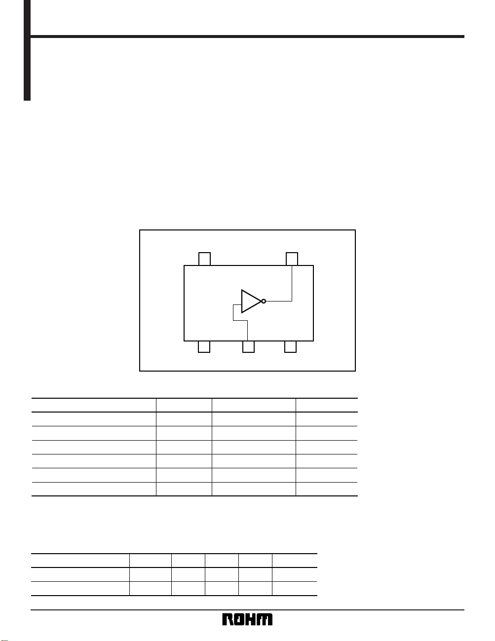
Block diagram
54
123
V
DD Y
NC A V
SS
•
Absolute maximum ratings (Ta = 25°C)
Parameter Symbol Limits Unit
Power supply voltage V
DD VSS – 0.3 ~ VSS + 18 V
Power dissipation Pd 170 mW
Input current I
IN ± 10 mA
Operating temperature Topr – 40 ~ + 85 °C
Storage temperature Tstg – 55 ~ + 150 °C
Input voltage V
IN VSS – 0.3 ~ VDD + 0.3 V
∗1 These values indicate the range limits of the voltage that can be applied to each pin without
destroying it. Operation is not guaranteed at these values.
∗
2 Power dissipation is reduced by 1.7mW for each increase in Ta of 1°C over 25°C.
•
Recommended operating conditions (Ta = 25°C, VSS = 0V)
Parameter Symbol Min. Typ. Max. Unit
Power supply voltage V
DD 3 — 16 V
Input voltage V
IN 0 — VDD V

2
Standard ICs BU4SU69
•
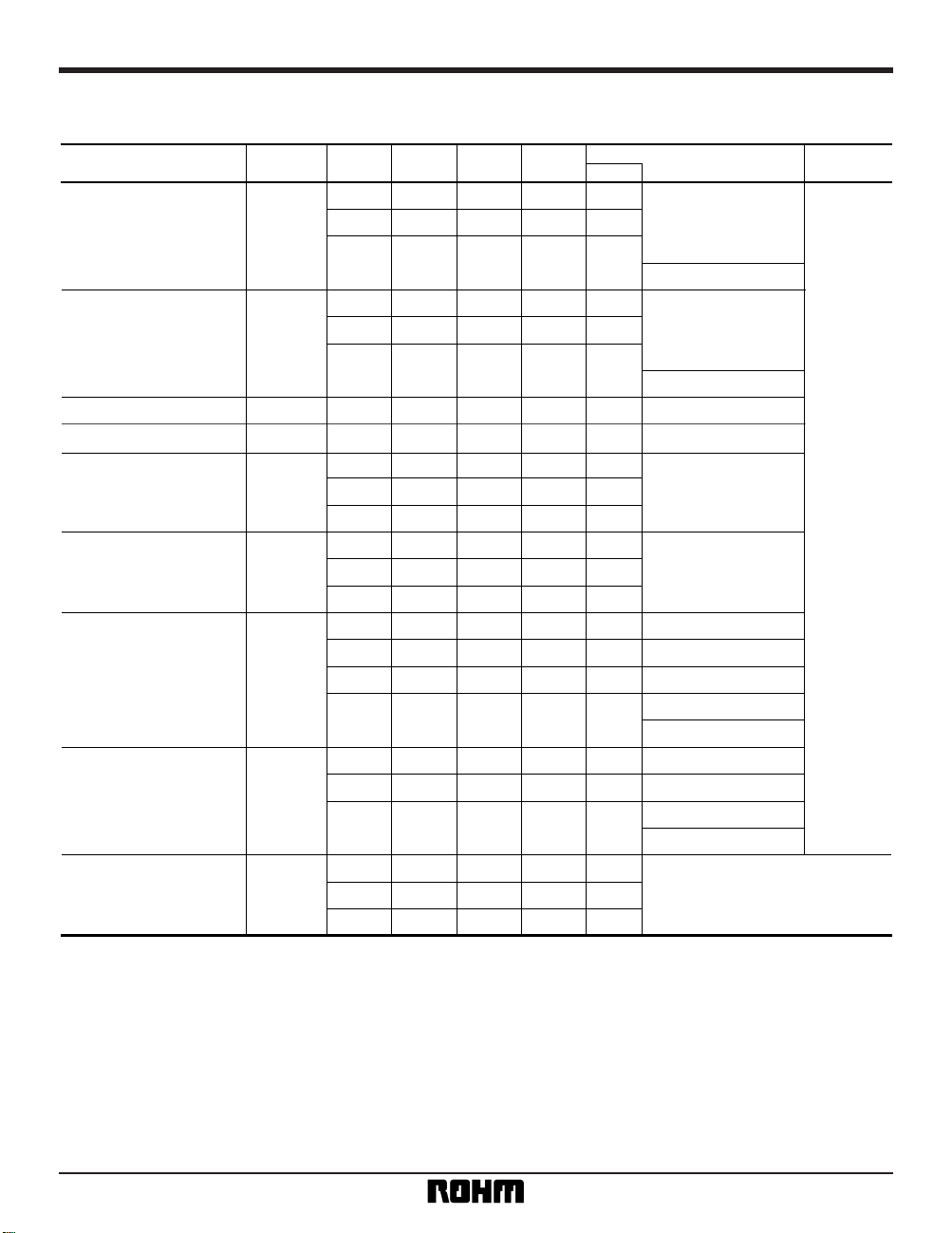
Electrical characteristics
DC characteristics (unless otherwise noted, V
SS = 0V, Ta = 25°C)
Parameter Symbol Min. Typ. Max. Unit
Measurement
circuit
VDD (V)
Input high level voltage V
IH
4.0 — — V 5
V
OUT = 0.5V
V
OUT = 1.0V
V
OUT = 1.5V
Fig.1
8.0 — — V 10
12.0 — — V 15
| I
OUT | < 1µ
A
Input low level voltage
V
IL
— — 1.0 V 5
V
OUT = 4.5V
V
OUT = 9.0V
V
OUT = 13.5V
— — 2.0 V 10
— — 3.0 V 15
| I
OUT | < 1µ
A
Input high level current I
IH — — 0.3
µ
A15VIH = 15V
Input low level current I
IL — — – 0.3
µ
A15VIL = 0V
Output high level voltage V
OH
4.95 — — V 5
| I
OUT | < 1µ
A
V
IN = VSS
9.95 — — V 10
14.95 — — V 15
Output low level voltage V
OL
— — 0.05 V 5
| I
OUT | < 1µ
A
V
IN = VDD
— — 0.05 V 10
— — 0.05 V 15
I
OH
– 0.51 — — mA 5 VOH = 4.6V
– 2.1 — — mA 5 V
OH = 2.5V
– 1.3 — — mA 10 V
OH = 9.5V
– 3.4 — — mA 15
V
OH = 13.5V
V
IN = VSS
IOL
0.51 — — mA 5 VOL = 0.4V
1.3 — — mA 10 V
OL = 0.5V
3.4 — — mA 15
V
OL = 1.5V
V
IN = VDD
Static current dissipation IDD
— — 0.25
µ
A5
V
IN = VSS, VDD— — 0.5
µ
A10
— — 1.0
µ
A15
Conditions
Output high level current
Output low level current
 Loading...