ROHM BU4S66 Datasheet

1
Standard ICs
Single analog switch
BU4S66
The BU4S66 is an ultra-compact IC with one circuit of the bi-directional analog switch BU4066B built into an SMP
package. Setting the enable input (CONT) to the "H" level sets the impedance between the switch input and the output pins low (ON state) and setting CONT to the "L" level sets the impedance high (OFF state).
•
Features
1) Low current dissipation.
2) Super-mini mold package designed for surface
mounting.
3) Wide range of operating power supply voltage.
4) Direct drive of 2 L-TTL inputs and 1 LS-TTL input.
•
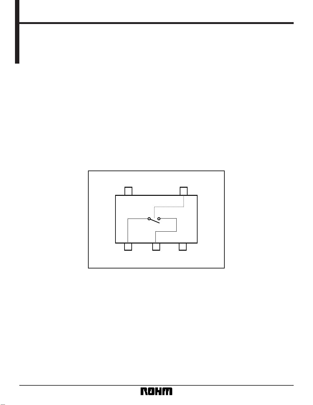
Block diagram
54
123
V
DD CONT
I / O O / I V
SS

2
Standard ICs BU4S66
•
Absolute maximum ratings (Ta = 25°C)
Parameter Symbol Limits Unit
V
DD VSS – 0.3 ~ VSS + 18 V
170 mW
I
IN ± 10 mA
°C
°C
V
IN VSS – 0.3 ~ VDD + 0.3 V
– 55 ~ + 150
– 40 ~ + 85
Pd
Topr
Tstg
Power supply voltage
Power dissipation
Input current
Operating temperature
Storage temperature
Input voltage
∗
1 These values indicate the range limits of the voltage that can be applied to each pin without
destroying it. Operation is not guaranteed at these values.
∗
2 Reduced by 1.7mW for each increase in Ta of 1°C over 25°C.
•
Recommended operating conditions (Ta = 25°C, VSS = 0V)
Parameter Symbol Min. Typ. Max. Unit
V
DD 3 — 16 V
V
IN 0—VDD V
Power supply voltage
Input voltage
•
Electrical characteristics
DC characteristics (unless otherwise noted, V
SS = 0V, Ta = 25°C)
Parameter Symbol Min. Typ. Max. Unit
Measurement
circuit
V
DD
(V)
Control input high level
voltage
V
IH
3.5 — — V 5
Current between input
and output = 10µA
Current between input
and output = 10µA
Fig.1
7.0 — — V 10
11.0 — — V 15
Control input low level
voltage
V
IL
— — 1.5 V 5
— — 3.0 V 10
— — 4.0 V 15
ON resistance R
ON
— 290 950 Ω 5
R
L = 10kΩ
0 ⬉ V
IN ⬉ VDD
Fig.2— 120 250 Ω 10
— 85 160 Ω 15
OFF-channel
leakage current
I
off
— — 0.3
µA
15
Fig.3
— — – 0.3 15
Static current dissipation
I
DD
— — 1.0
µA
5
V
IN = VDD or GND —— — 2.0 10
— — 4.0 15
Input capacitance
(control input)
C
C — 8 — pF — f = 1MHz —
Input capacitance
(switch input)
C
S — 10 — pF — f = 1MHz —
Conditions
= 0V, V
OUT = 15V
V
IN
VIN
= 15V, VOUT = 0V
 Loading...