

1
Standard ICs
Hex Schmitt trigger
BU4584B / BU4584BF / BU4584BFV
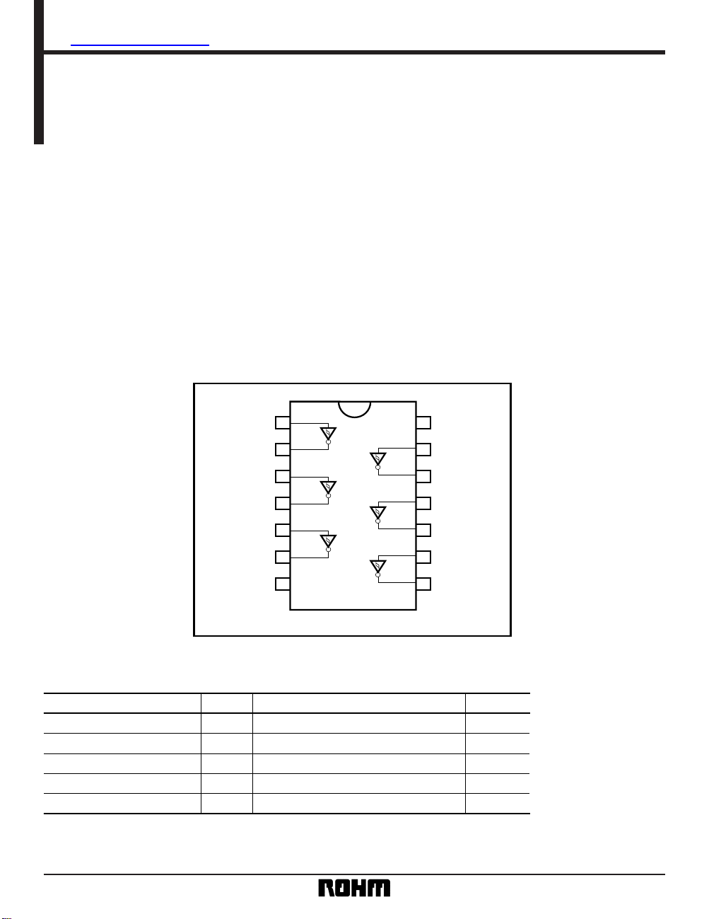
The BU4584B, BU4584BF, and BU4584BFV are inverter-type Schmitt trigger circuits, with six circuits mounted on a
single chip. These are ideal when enhanced noise immunity is required, and when wave form rectification circuits
with slow rise or fall input times are involved.
•
Features
1) Low power dissipation.
2) Wide range of operating power supply voltage.
3) High input impedance.
4) High fan-out.
5) Direct drive of 2 L-TTL inputs and LS-TTL input.
•
Block diagram
1
I
1
2
O
1
3
I
2
4
O
2
5
I
3
6
O
3
7
14
13
12
11
10
9
8
V
SS
VDD
I6
O6
I5
O5
I4
O4
•
Absolute maximum ratings (VSS = 0v, Ta = 25°C)
Parameter Symbol Limits Unit
V
DD V
mW
°C
°C
V
IN V
– 0.3 ~ + 18
Pd
Topr
Tstg
1000 (DIP), 450 (SOP), 350 (SSOP)
Power supply voltage
Power dissipation
Operating temperature
Storage temperature
Input voltage
– 0.3 ~ V
DD + 0.3
– 40 ~ + 85
– 55 ~ + 150
查询BU4584供应商

2
Standard ICs BU4584B / BU4584BF / BU4584BFV
Parameter Symbol Min. Typ. Max. Unit Conditions
Measurement
circuit
VDD (V)
V
IH
3.5
——
V
5
—
7.0
——
10
11.0
——
15
V
IL
——
1.5
V
5
———
3.0 10
——
4.0 15
I
IH
——
0.3 µ
A15V
IH = 15V
I
IL
——
– 0.3 µ
A15V
IL = 0V
V
OH
4.95
——
V
5
I
O = 0mA
Fig.1
109.95
——
1514.95
——
V
OL
——
0.05
V
5
I
O = 0mA10
——
0.05
15
——
0.05
I
OH
– 0.44
——
mA
5VOH = 4.6V
V
OH = 9.5V
V
OH = 13.5V
10– 1.1
——
15– 3.0
——
I
OL
0.44
——
mA
5V
OL = 0.4V
V
OL = 0.5V
V
OL = 1.5V
101.1
——
153.0
——
I
DD
——
1
µ
A
5
————
210
——
45
V
H
0.15
—
0.6
V
5
—
Fig.1100.25
—
1.0
150.40
—
1.5
Input high level voltage
Input low level voltage
Input high level current
Input low level current
Output high level voltage
Output low level voltage
Output high level current
Output low level current
Static current
consumption
Hysteresis voltage
•
Electrical characteristics
DC characteristics (unless otherwise noted, V
SS = 0V, Ta = 25°C)
Switching characteristics (unless otherwise noted, Ta = 25°C, V
SS = 0 V, CL =50pF)
Parameter Symbol Min. Typ. Max. Unit Conditions
Measurement
circuit
VDD (V)
t
TLH
100
—
ns
5
—
Fig.250
—
10
40
—
15
t
THL
100
—
ns
5
—
Fig.250
—
10
40
—
15
t
PLH
125
—
ns
5
—
Fig.260
—
10
50
—
15
t
PHL
125
—
ns
5
—
Fig.260
—
10
50
—
—
—
—
—
—
—
—
—
—
—
—
—
15
Output rise time
Output fall time
Propagation delay time,
"L" to "H"
Propagation delay time,
"H" to "L"
3
Standard ICs BU4584B / BU4584BF / BU4584BFV
•
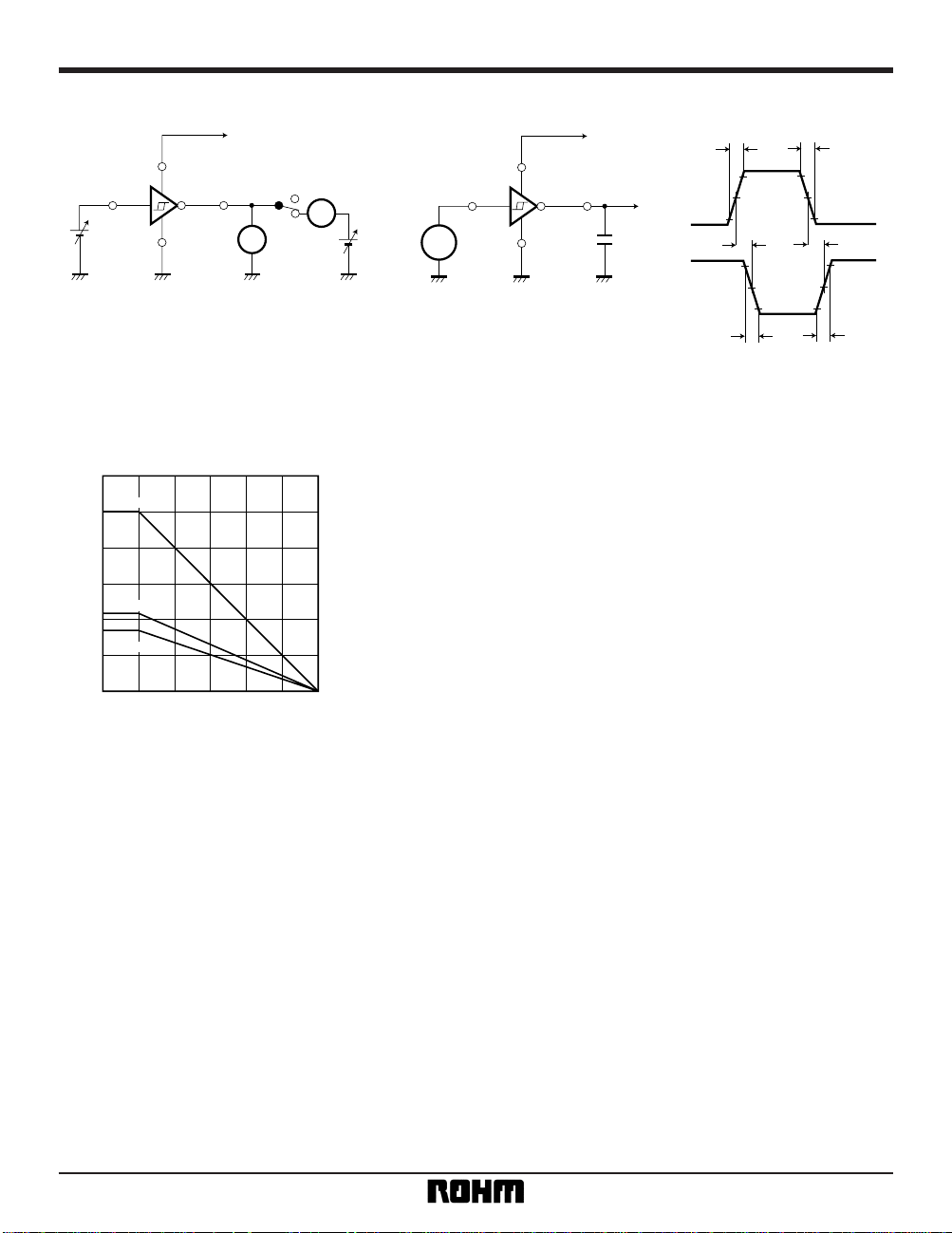
Measurememt circuits
V
A
VDD
Fig.1 DC characteristics
GND
CL
P. G.
VDD
20ns
20ns
t
PHL
tPLH
tTHL
tTLH
Input
Output
Fig.2 Switching characteristics
GND
•
Electrical characteristic curve
POWER DISSIPATION: Pd (mW)
1200
1000
800
600
400
200
0
0 25 50 75 100 125 150
AMBIENT TEMPERATURE: Ta (°C)
SOP14
SSOP-B14
DIP14
Fig.3 Power dissipation vs. Ta

4
Standard ICs BU4584B / BU4584BF / BU4584BFV
•
External dimensions (Units: mm)
BU4584B
BU4584BFV
BU4584BF
DIP14
SSOP-B14
SOP14
6.5 ± 0.3
19.4 ± 0.3
0.5 ± 0.1
3.2 ± 0.2
4.25 ± 0.3
14 8
71
0.3 ± 0.1
0.51Min.
7.62
0° ~ 15°
2.54
0.4
± 0.11.27
1
14
8.7 ± 0.2
7
8
4.4 ± 0.2
6.2 ± 0.3
0.11
1.5 ± 0.1
0.15
0.15 ± 0.1
0.3Min.
0.1
0.22 ± 0.1
0.65
8
7
14
1
6.4 ± 0.3
4.4 ± 0.2
5.0 ± 0.2
1.15 ± 0.1
0.15 ± 0.1
0.3Min.
0.1
 Loading...