

Page 1
General-purpose CMOS Logic IC Series (BU4S,BU4000B Series)
High Voltage CMOS Logic ICs
<Analog Switch>
BU4066BC,BU4066BCF,BU4066BCFV,BU4051BC,
BU4051BCF,BU4051BCFV,BU4052BC,BU4052BCF,BU4052BCFV,
BU4053BC,BU4053BCF,BU4053BCFV,BU4551B,BU4551BF,BU4551BFV
●Description
BU4066BC series ICs each contain 4 independent switches capable of controlling either digital or analog signals.
BU4051BC / BU4052BC / BU4053BC / and BU4551B series ICs are analog selectable composite multiplexer/demultiplexer.
BU4051BC series is configured with 8 channels, BU4052BC is configured with two 4 channels,BU4053BC series is
configured with three 2 channels, BU4551B series is configured with four 2 channels, and s witches applicable for each
channel are turned on according to digital signals of control terminal. Even if the log ic amplitude (VDD-VSS) of the control
signal is small, signals of large amplitude (VDD-VEE) can be switched.
●Features
1) Low power consumption
2) Wide operating supply voltage (3[V]~18[V])
3) High input impedance
4) L-TTL2 input and LS-TTL1 can be driven directly.
5) Applicable channel switches can be turned “ON” and “OFF” by the digital control signal.
6) Small control voltage (VDD-VSS) can control signals of large amplitude (VDD-VEE).
7) Linearity with excellent transfer characteristics
●Use
This product is used as the switch and chopper modulation circuit of analog and digital signals.
Since ON resistance of each switch is low, the product can be connected to low impedance circuit.
The product can be used as ON/OFF switch and changeover switch of high-speed lines without degradi ng analog signals
such as voice and images.
●Lineup
High Voltage CMOS Logic
Analog Switch
4
circuits
1
circuits
2
circuits
3
circuits
4
circuits
switch
8 to 1
multiplexer
4 to 1
multiplexer
2 to 1
multiplexer
2 to 1
multiplexer
BU4066BC/
BU4066BCF/
BU5066BCFV
BU4051BC/
BU4051BCF/
BU4051BCFV
BU4052BC/
BU4052BCF/
BU4052BCFV
BU4053BC/
BU4053BCF/
BU4053BCFV
BU4551B/
BU4551B F/
BU4551B FV
(Quad-analog switch)
(8ch analog multiplexer/demultiplexer)
(Dual 4ch analog multiplexer/demultiplexer)
(Triple 2ch analog multiplexer/demultiplexer)
(Quad 2ch analog multiplexer/demultiplexer)
No.11050EBT05
www.rohm.com
© 2011 ROHM Co., Ltd. All rights reserved.
1/17
2011.08 - Rev.B
Page 2
BU4066BC,BU4066BCF,BU4066BCFV,BU4051BC,BU4051BCF,BU4051BCFV,BU4052BC,
BU4052BCF,BU4052BCFV,BU4053BC,BU4053BCF,BU4053BCFV,BU4551B,BU4551BF,BU4551BFV
Technical Note
●Absolute Maximum Ratings
Parameter Symbol
BU4066BC BU4051BC BU4052BC BU4053BC BU4551B
Limit Unit
Power Supply Voltage VDD -0.5 to 20 -0.3 to 18 V
Supply current Iin ±10 mA
Operating temperature Topr -40 to 85 ℃
Storage temperature Tstg -55 to 150 ℃
Input Voltage VIN -0.5 to VDD+0.5 -0.3 to VDD+0.3 V
Maximum junction temperature Tjmax 150 ℃
●Recommended Operating Conditions
Parameter
Symbol
BU4066BC BU4051BC BU4052BC BU4053BC BU4551B
Limit
Operating Power Supply VDD 3 to 18 3 to 16 V
Input Voltage VIN 0 to VDD V
●Thermal Derating Curve
1400
1200
〕
1000
mW
〔
Pd
800
1180[mV] BU4066BC (*1)
870[mV] BU4066BCFV (*2)
610[mV] BU4066BCF (*3)
600
Dissipation
400
Power
200
0
0 25 50 75 100 125 150 175
Ambient temperature Ta
85℃
●I/O Interface
〔℃〕
VDD
1400
1200
〕
1000
mW
〔
Pd
800
600
Dissipation
400
Power
200
0
0 25 50 75 100 125 150 175
1250[mV] BU4*** (*4)
620[mV] BU4***FV (*5)
380[mV] BU4***F (*6)
(*) Below shows BU4***
85℃
Ambient temperature Ta
〔℃〕
VDD VDD
BU4051BC
BU4052BC
BU4053BC
BU4551B
(*1) 9.5
(*2) 7.0
(*3) 4.9
(*4) 10.0
mW/℃
(*5) 5.0
(*6) 3.1
When used at Ta=25[°C] or above,
values of above are reduced per 1[°C].
Allowable loss is the value for mounting
70[mm] x 70[mm] x 1.6[mm] FR4 glass epoxy
circuit board copper foil area is 3% or less).
<Analog switch input / output>
GND
GND
<Input>
GND
●Description of output rising / falling wave
・tPLH: Time up to 50% of the rise time of input waveform
~ 50% of the rise time of output waveform
・tPHL: Time up to 50% of the fall time of input waveform
~ 50% of the fall time of output waveform
・tPZH: Time up to 50% of input ~ 50% of the
rise time of output waveform
・tPHZ: Time up to 50% of input ~ 50% of the
fall time of output waveform
・tPZH: Time up to 50% of input ~ 50% of the
fall time of output waveform
・tPHZ: Time up to 10% of input ~ 10% of the
rise time of output waveform
Unit
www.rohm.com
© 2011 ROHM Co., Ltd. All rights reserved.
2/17
2011.08 - Rev.B
Page 3

BU4066BC,BU4066BCF,BU4066BCFV,BU4051BC,BU4051BCF,BU4051BCFV,BU4052BC,
BU4052BCF,BU4052BCFV,BU4053BC,BU4053BCF,BU4053BCFV,BU4551B,BU4551BF,BU4551BFV
●Electrical Characteristics(BU4066BC)
DC Characteristics(Unless otherwise noted, VSS=0[V],Ta=25[℃])
Parameter Symbol
Input “H” voltage VIH
Input “L” voltage VIL
Input “H” current IIH - - 0.3 μA 15 VIH=15[V] Input “L” current IIL - - -0.3 μA 15 VIL=0[V] -
ON resistance RON
ON resistance defluxion △RON
Channel-OFF
Leakage current
Static supply current IDD
Input capacitance
(control input)
Input capacitance
(switch input)
Switching Characteristics(Unless otherwise noted, VSS=0[V],Ta=25[℃],CL=50[pF])
Parameter Symbol
Propagation delay time
SWIN→OUT
Propagation delay time
CONT→OUT
Propagation delay time
CONT→OUT
Feed through attenuation FT - 0.7 - MHz 5
Sine wave distortion D - 0.1 - % 5
Cross talk
(CONT→OUT)
Cross talk(2)
Between channels
IOFF
CC - 8 - pF - f=1[MHz] -
CS - 10 - pF - f=1[MHz] -
tPLH
tPHL
tPHZ,tPLZ
tPZH,tPZL
tPHZ,tPLZ
tPZH,tPZL
CTc - - 600 mVp-p 5
CT - 1 - MHz 5
Standard Value
MIN TYP MAX VDD[V]
3.5 - -
11.0 - - 15
- - 1.5
- - 3.75 15
- 150 600
- 500 950 5
200 600 5
120 500 10
- 80 280 15
- 25 -
- 5 - 15
- - 0.3
- - -0.3 15
- - 1.0
- - 4.0 15
Standard Value
MIN TYP MAX
- 20 50
- 12 40 10
- 10 30 15
- 40 90
- 35 80 10
- 30 70 15
- 60 140
- 20 50 10
- 15 40 15
Unit
V
V
Ω
Ω
μA
μA
Unit
ns
ns
ns
5
5
5
5
15
5
VDD[V]
5
5
5
VIN=0.25[V]
RL=10[kΩ]
VIN=2.5[V]
RL=10[kΩ]
VIN=5[V]
RL=10[kΩ]
VIN=5[V]
RL=10[kΩ]
VIN=7.5[V]
RL=10[kΩ]
VI=VDD/2
RL=10[kΩ]
VIN=15[V]
VOUT=0[V]
VIN=0[V]
VOUT=15[V]
VI=VDD or GND - - - 2.0 10
RL=10[kΩ] 2・3
Output“H”“L”
→“Hi Z”
RL=1[kΩ]
Output“Hi Z”
→“H”“L”
RL=1[kΩ]
VSS=-5[V]
RL=10[kΩ]
VSS=-5[V]
RL=10[kΩ]
VSS=-5[V]
RL=10[kΩ],f=1[MHz]
VSS=-5[V]
RL=10[kΩ]
Technical Note
Condition Fig.No
- - 7.0 - - 10
- - - - 3.0 10
Condition Fig.No
1
- - 10 - 10
-
4・5
6・7
-
-
-
-
www.rohm.com
© 2011 ROHM Co., Ltd. All rights reserved.
3/17
2011.08 - Rev.B
Page 4

BU4066BC,BU4066BCF,BU4066BCFV,BU4051BC,BU4051BCF,BU4051BCFV,BU4052BC,
BU4052BCF,BU4052BCFV,BU4053BC,BU4053BCF,BU4053BCFV,BU4551B,BU4551BF,BU4551BFV
●Electrical Characteristics(BU4051BC)
DC Characteristics(Unless otherwise noted, VSS=0[V],Ta=25[℃])
Parameter Symbol
Input “H” voltage VIH
Input “L” voltage VIL
Input “H” current IIH - - 0.3 μA 15 VIH=15[V] Input “L” current IIL - - -0.3 μA 15 VIL=0[V] -
ON resistance RON
ON resistance defluxion △RON
Channel-OFF
Leakage current
Static supply current IDD
Switching Characteristics(Unless otherwise noted, VSS=0[V],Ta=25[℃],CL=50[pF])
Parameter Symbol
Propagation delay time
CHANNEL IN→OUT
Propagation delay time
CONT→OUT
Propagation delay time
INHIBIT→OUT
Maximum propagation
frequency
Feed through attenuation FT - 0.5 - MHz 5 VEE=-5[V] Sine wave distortion D - 0.02 - % 5 VEE=-5[V] Input capacitance
(control input)
Input capacitance
(switch input)
IOFF
tPLH
tPHL
tPHZ,tPLZ
tPZH,tPZL
tPHZ,tPLZ
tPZH,tPZL
fMAX. - 20 - MHz 5 VEE=-5[V] -
CC - 5 - pF - - -
CS - 10 - pF - - -
Standard Value
MIN TYP MAX VDD[V]
3.5 - -
11.0 - - 15
- - 1.5
- - 4.0 15
- - 950
- - 160 15
- 10 -
- 4 - 15
- - 0.3
- - -0.3 15
- - 5
- - 15 15
Standard Value
MIN TYP MAX VDD[V]
- 15 45
- 8 20 10
- 6 15 15
- 170 550
- 90 240 10
- 70 160 15
- 150 450
- 70 210 10
- 50 160 15
Unit
V
V
Ω
Ω
μA
μA
Unit
ns
ns
ns
5
5
5
5
15
5
VI=VDD or GND - - - 10 10
5
5
5
Technical Note
Condition Fig.No
- - 7.0 - - 10
- - - - 3.0 10
- 8 - - 250 10
- - - 6 - 10
- -
Condition Fig.No
- 9・10
-
-
11・12
13・14
15・16
17・18
www.rohm.com
© 2011 ROHM Co., Ltd. All rights reserved.
4/17
2011.08 - Rev.B
Page 5

BU4066BC,BU4066BCF,BU4066BCFV,BU4051BC,BU4051BCF,BU4051BCFV,BU4052BC,
BU4052BCF,BU4052BCFV,BU4053BC,BU4053BCF,BU4053BCFV,BU4551B,BU4551BF,BU4551BFV
●Electrical Characteristics(BU4052BC)
DC Characteristics(Unless otherwise noted, VSS=0[V],Ta=25[℃])
Parameter Symbol
Input “H” voltage VIH
Input “L” voltage VIL
Input “H” current IIH - - 0.3 μA 15 VIH=15[V] Input “L” current IIL - - -0.3 μA 15 VIL=0[V] -
ON resistance RON
ON resistance defluxion △RON
Channel-OFF
Leakage current
Static supply current IDD
Switching Characteristics(Unless otherwise noted, Ta=25℃,CL=50pF)
Parameter Symbol
Propagation delay time
SWITCH IN→OUT
Propagation delay time
CONT→OUT
Propagation delay time
INH→OUT
Maximum propagation
frequency
Feed through attenuation FT - 0.5 - MHz 5 VEE=-5[V] Sine wave distortion D - 0.02 - % 5 VEE=-5[V] Input capacitance
(control input)
Input capacitance
(switch input)
IOFF
tPLH
tPHL
tPHZ,tPLZ
tPZH,tPZL
tPHZ,tPLZ
tPZH,tPZL
fMAX. - 20 - MHz 5 VEE=-5[V] -
CC - 5 - pF - - -
CS - 10 - pF - - -
Standard Value
MIN TYP MAX VDD[V]
3.5 - -
11.0 - - 15
- - 1.5
- - 4.0 15
- - 950
- - 160 15
- 10 -
- 4 - 15
- - 0.3
- - -0.3 15
- - 5
- - 15 15
Standard Value
MIN TYP MAX VDD[V]
- 15 45
- 8 20 10
- 6 15 15
- 170 550
- 90 240 10
- 70 160 15
- 150 450
- 70 210 10
- 50 160 15
Unit
V
V
Ω
Ω
μA
μA
Unit
ns
ns
ns
5
5
5
5
15
5
VI=VDD or GND - - - 10 10
5
5
5
Technical Note
Condition Fig.No
- - 7.0 - - 10
- - - - 3.0 10
- 19 - - 250 10
- - - 6 - 10
- -
Condition Fig.No
- 20・21
-
-
22・23
24・25
26・27
28・29
www.rohm.com
© 2011 ROHM Co., Ltd. All rights reserved.
5/17
2011.08 - Rev.B
Page 6

BU4066BC,BU4066BCF,BU4066BCFV,BU4051BC,BU4051BCF,BU4051BCFV,BU4052BC,
BU4052BCF,BU4052BCFV,BU4053BC,BU4053BCF,BU4053BCFV,BU4551B,BU4551BF,BU4551BFV
●Electrical Characteristics(BU4053BC)
DC Characteristics(Unless otherwise noted, VSS=0[V],Ta=25[℃])
Parameter Symbol
Input “H” voltage VIH
Input “L” voltage VIL
Input “H” current IIH - - 0.3 μA 15 VIH=15[V] Input “L” current IIL - - -0.3 μA 15 VIL=0[V] -
RON resistance RON
RON resistance defluxion △RON
Channel-OFF
Leakage current
Static supply current IDD
Switching Characteristics(Unless otherwise noted, VSS=0[V],Ta=25[℃],CL=50[pF])
Parameter Symbol
Propagation delay time
SW IN→OUT
Propagation delay time
CONT→OUT
Propagation delay time
INH→OUT
Maximum propagation
frequency
Feed through attenuation FT - 0.7 - MHz 5 VEE=-5[V] Sine wave distortion D - 0.02 - % 5 VEE=-5[V] Input capacitance
(control input)
Input capacitance
(switch input)
IOFF
tPLH
tPHL
tPHZ,tPLZ
tPZH,tPZL
tPHZ,tPLZ
tPZH,tPZL
fMAX. - 20 - MHz 5 VEE=-5[V] -
CC - 5 - pF - - -
CS - 10 - pF - - -
Standard Value
MIN TYP MAX VDD[V]
3.5 - -
11.0 - - 15
- - 1.5
- - 4.0 15
- - 950
- - 160 15
- 10 -
- 4 - 15
- - 0.3
- - -0.3 15
- - 5
- - 15 15
Standard Value
MIN TYP MAX VDD[V]
- 15 45
- 8 20 10
- 6 15 15
- 170 550
- 90 240 10
- 70 160 15
- 150 380
- 70 200 10
- 50 160 15
Unit
V
V
Ω
Ω
μA
μA
Unit
ns
ns
ns
5
5
5
5
15
5
VI=VDD or GND - - - 10 10
5
5
5
Technical Note
Condition Fig.No
- - 7.0 - - 10
- - - - 3.0 10
- 30 - - 250 10
- - - 6 - 10
- -
Condition Fig.No
- 31・32
-
-
33・34
35・36
37・38
39・40
www.rohm.com
© 2011 ROHM Co., Ltd. All rights reserved.
6/17
2011.08 - Rev.B
Page 7

BU4066BC,BU4066BCF,BU4066BCFV,BU4051BC,BU4051BCF,BU4051BCFV,BU4052BC,
BU4052BCF,BU4052BCFV,BU4053BC,BU4053BCF,BU4053BCFV,BU4551B,BU4551BF,BU4551BFV
●Electrical Characteristics(BU4551BC)
DC Characteristics(Unless otherwise noted, VSS=0[V],Ta=25[℃])
Parameter Symbol
Input “H” voltage VIH
Input “L” voltage VIL
Input “H” current IIH - - 0.3 μA 15 VIH=15[V] Input “L” current IIL - - -0.3 μA 15 VIL=0[V] -
ON resistance RON
ON resistance defluxion △RON
Channel-OFF
Leakage current
Static supply current IDD
Switching Characteristics(Unless otherwise noted, VSS=0[V],Ta=25[℃],CL=50[pF])
Parameter Symbol
Propagation delay time
SW IN→OUT
Propagation delay time
CONT→OUT
Propagation delay time
INH→OUT
Maximum propagation
frequency
Feed through attenuation FT - 0.7 - MHz - VEE=-5[V] Sine wave distortion D - 0.02 - % - VEE=-5[V] Input capacitance
(control input)
Input capacitance
(switch input)
IOFF
tPLH
tPHL
tPZH
tPHZ
tPZL
tPLZ
fMAX. - 15 - MHz - VEE=-5[V] -
CC - 5 - pF - - -
CS - 10 - pF - - -
Standard Value
MIN TYP MAX VDD[V]
3.5 - -
11.0 - - 15
- - 1.5
- - 4.0 15
- - 1100
- - 280 15
- 25 -
- 5 - 15
- - 0.3
- - -0.3 15
- - 5
- - 15 15
Standard Value
MIN TYP MAX VDD[V]
- 35 -
- 15 - 10
- 12 - 15
- 360 -
- 160 - 10
- 120 - 15
- 360 -
- 160 - 10
- 120 - 15
Unit
V
V
Ω
Ω
μA
μA
Unit
ns
ns
ns
5
5
5
5
15
5
VI=VDD or GND - - - 10 10
5
5
5
Technical Note
Condition Fig.No
- - 7.0 - - 10
- - - - 3.0 10
- 41 - - 500 10
- - - 10 - 10
- -
Condition Fig.No
- 42・43
- 44・45
- 46・47
www.rohm.com
© 2011 ROHM Co., Ltd. All rights reserved.
7/17
2011.08 - Rev.B
Page 8

BU4066BC,BU4066BCF,BU4066BCFV,BU4051BC,BU4051BCF,BU4051BCFV,BU4052BC,
BU4052BCF,BU4052BCFV,BU4053BC,BU4053BCF,BU4053BCFV,BU4551B,BU4551BF,BU4551BFV
Technical Note
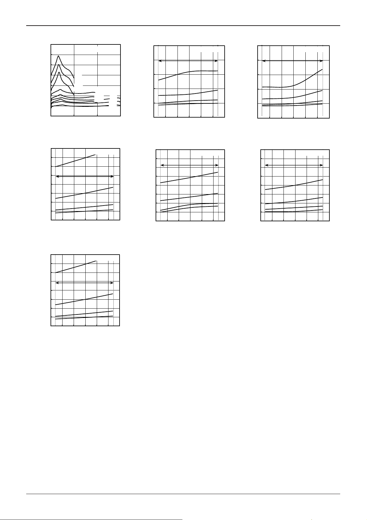
●Reference Data(BU4066BC)
300
250
200
150
100
ON Resistance [Ω]
VDD=5[V]
85[℃]
25[℃]
-40[℃]
50
[BU4066BC/F/FV]
VDD=10[V]
85[℃]
25[℃]
-40[℃]
0
0 5 10 15
Input Voltage [V]
Fig.1 On resistance-input voltage
200
175
150
125
100
75
Propagation Delay [ns]
50
25
0
200
175
150
125
100
75
Propagation Delay [ns]
50
25
0
Fig.7 falling propagation delay
Operating Temperature Range
-50 - 25 0 25 50 75 100
Ambient Temperature [℃]
Fig.4 rising propagation delay
(CONT-OUT ,tPZH)
Operating Temperature Range
-50 - 25 0 25 50 75 100
Ambient Temperature [℃]
(CONT-OUT ,tPZL)
VDD=3[V]
VDD=5[V]
VDD=10[V]
VDD=18[V]
VDD=3[V]
VDD=5[V]
VDD=10[V]
VDD=18[V]
[BU4066BC/F/FV]
[BU4066BC/F/FV]
VDD=15[V]
85[℃]
25[℃]
-40[℃]
50
40
30
20
Propagation Delay [ns]
10
0
Operating Temperature Range
-50 -25 0 25 50 75 100
Ambient Temperature [℃]
[BU4066BC/F/FV]
VDD=3[V]
VDD=5[V]
VDD=10[V]
VDD=18[V]
Fig.2 rising propagation delay
(IN-OUT)
200
175
150
125
100
75
Propagation Delay [ns]
50
25
0
-50 -25 0 25 50 75 100
[BU4066BC/F/FV]
Operating Temperature Range
VDD=3[V]
VDD=5[V]
VDD=10[V]
VDD=18[V]
Ambient Temperature [℃]
Fig.5 falling propagation delay
(CONT-OUT ,tPHZ)
50
40
30
20
Propagation Delay [ns]
10
0
Operating Temperature Range
-50 -25 0 25 50 75 100
Ambient Temperature [℃]
[BU4066BC/F/FV]
VDD=3[V]
VDD=5[V]
VDD=10[V]
VDD=18[V]
Fig.3 falling propagation delay
(IN-OUT)
200
175
150
125
100
Propagation Delay [ns]
75
50
25
0
Operating Temperature Range
-50 - 25 0 25 50 75 100
Ambient Temperature [℃]
[BU4066BC/F/FV]
VDD=3[V]
VDD=5[V]
VDD=10[V]
VDD=18[V]
Fig.6 rising propagation delay
(CONT-OUT ,tPLZ)
www.rohm.com
© 2011 ROHM Co., Ltd. All rights reserved.
8/17
2011.08 - Rev.B
Page 9

BU4066BC,BU4066BCF,BU4066BCFV,BU4051BC,BU4051BCF,BU4051BCFV,BU4052BC,
BU4052BCF,BU4052BCFV,BU4053BC,BU4053BCF,BU4053BCFV,BU4551B,BU4551BF,BU4551BFV
Technical Note
●Reference Data(BU4051BC)
300
250
VDD=5[V]
200
150
85[℃]
25[℃]
-40[℃]
100
ON Resistance [Ω]
50
0
0 5 10 15
Input Voltage [V]
Fig.8 ON resistance-input voltage
500
400
300
Operating Temperature Range
VDD=10[V]
VDD=3[V]
[BU4051BC/F/FV]
85[℃]
25[℃]
-40[℃]
[BU4051BC/F/FV]
200
Propagation Delay [ns]
100
0
-50 -25 0 25 50 75 100
Fig.11 propagation delay time tPZH
500
400
300
VDD=5[V]
VDD=10[V]
VDD=18[V]
Ambient Temperature [℃]
(CONT-OUT)
[BU4051BC/F/FV] [BU4051BC/F/FV]
Operating Temperature Range Operating Temperature Range
VDD=3[V]
200
Propagation Delay [ns]
100
0
-50 - 25 0 25 50 75 100
Ambient Temperature [℃]
Fig.14 propagation delay time tPZL
500
400
300
200
Propagation Delay [ns]
100
0
Fig.17 propagation delay time tPZL
Operating Temperature Range
-50 - 25 0 25 50 75 100
Ambient Temperature [℃]
VDD=5[V]
VDD=10[V]
VDD=18[V]
(CONT-OUT)
[BU4051BC/F/FV] [BU4051BC/F/FV]
VDD=3[V]
VDD=5[V]
VDD=10[V]
VDD=18[V]
(INH-OUT)
VDD=15[V]
85[℃]
25[℃]
-40[℃]
50
40
30
20
Propagation Delay [ns]
10
0
Operating Temperature Range Operating Temperature Range
-50 -25 0 25 50 75 100
Ambient Temperature [℃]
[BU4051BC/F/FV] [BU4051BC/F/FV]
VDD=3[V]
VDD=5[V]
VDD=10[V]
VDD=18[V]
Fig.9 propagation delay time tPLH
(IN-OUT)
500
400
300
200
Propagation Delay [ns]
100
0
Operating Temperature Range Operating Temperature Range
-50 - 25 0 25 50 75 100
Ambient Temperature [℃]
[BU4051BC/F/FV] [BU4051BC/F/FV]
VDD=3[V]
VDD=5[V]
VDD=10[V]
VDD=18[V]
Fig.12 propagation delay time tPHZ
(CONT-OUT)
500
400
300
200
Propagation Delay [ns]
100
0
-50 - 25 0 25 50 75 100
VDD=3[V]
VDD=5[V]
VDD=10[V]
VDD=18[V]
Ambient Temperature [℃]
Fig.15 propagation delay time tPZH
(INH-OUT)
500
400
300
200
Propagation Delay [ns]
100
0
Operating Temperature Range
-50 - 25 0 25 50 75 100
Ambient Temperature [℃]
VDD=3[V]
VDD=5[V]
VDD=10[V]
VDD=18[V]
Fig.18 propagation delay time tPLZ
(INH-OUT)
50
40
30
20
Propagation Delay [ns]
10
0
-50 -25 0 25 50 75 100
Ambient Temperature [℃]
VDD=3[V]
VDD=5[V]
VDD=10[V]
VDD=18[V]
Fig.10 propagation delay time tPHL
(IN-OUT)
500
400
300
200
Propagation Delay [ns]
100
0
-50 - 25 0 25 50 75 100
VDD=10[V]
VDD=18[V]
Ambient Temperature [℃]
VDD=3[V]
VDD=5[V]
Fig.13 propagation delay time tPLZ
(CONT-OUT)
500
400
300
200
Propagation Delay [ns]
100
0
-50 - 25 0 25 50 75 100
[BU4051BC/F/FV]
VDD=3[V]
VDD=5[V]
VDD=10[V]
VDD=18[V]
Operating Temperature Range
Ambient Temperature [℃]
Fig.16 propagation delay time tPHZ
(INH-OUT)
www.rohm.com
© 2011 ROHM Co., Ltd. All rights reserved.
9/17
2011.08 - Rev.B
Page 10

BU4066BC,BU4066BCF,BU4066BCFV,BU4051BC,BU4051BCF,BU4051BCFV,BU4052BC,
BU4052BCF,BU4052BCFV,BU4053BC,BU4053BCF,BU4053BCFV,BU4551B,BU4551BF,BU4551BFV
●Reference Data(BU4052BC)
300
250
200
150
VDD=5[V]
85[℃]
25[℃]
-40[℃]
100
ON Resistance [Ω]
50
[BU4052BC/F/FV]
VDD=10[V]
85[℃]
25[℃]
-40[℃]
VDD=15[V]
85[℃]
25[℃]
-40[℃]
50
40
30
20
Propagation Delay [ns]
10
[BU4052BC/F/FV] [BU4052BC/F/FV]
Operating Temperature Range Operating Temperature Range
VDD=3[V]
VDD=5[V]
VDD=10[V]
VDD=18[V]
50
40
30
20
Propagation Delay [ns]
10
0
0 5 10 15
Input Voltage [V]
Fig.19 ON resistance-input voltage
500
400
300
200
Propagation Delay [ns]
100
[BU4052BC/F/FV]
VDD=3[V]
VDD=5[V]
VDD=10[V]
VDD=18[V]
0
-50 -25 0 25 50 75 100
Ambient Temperature [℃]
Fig.20 propagation delay time tPLH
(IN-OUT)
500
400
300
200
Propagation Delay [ns]
100
[BU4052BC/F/FV] [BU4052BC/F/FV]
VDD=3[V]
VDD=5[V]
VDD=10[V]
VDD=18[V]
0
-50 -25 0 25 50 75 100
Fig.21 propagation delay time tPHL
500
400
300
200
Propagation Delay [ns]
100
0
-50 - 25 0 25 50 75 100
Ambient Temperature [℃]
Fig.22 propagation delay time tPZH
(CONT-OUT)
500
400
300
200
Propagation Delay [ns]
100
0
-50 - 25 0 25 50 75 100
Ambient Temperature [℃]
VDD=3[V]
VDD=5[V]
VDD=10[V]
VDD=18[V]
Fig.25 propagation delay time tPZL
(CONT-OUT)
500
400
300
200
Propagation Delay [ns]
100
0
Fig.28 propagation delay time tPZL
Operating Temperature Range
-50 - 25 0 25 50 75 100
Ambient Temperature [℃]
VDD=3[V]
VDD=5[V]
VDD=10[V]
VDD=18[V]
(INH-OUT)
[BU4052BC/F/FV]
[BU4052BC/F/FV]
0
-50 - 25 0 25 50 75 100
Ambient Temperature [℃]
Fig.23 propagation delay time tPHZ
(CONT-OUT)
500
400
300
200
Propagation Delay [ns]
100
0
Operating Temperature Range Operating Te mperature Range
-50 - 25 0 25 50 75 100
Ambient Temperature [℃]
[BU4052BC/F/FV] [BU4052BC/F/FV]
VDD=3[V]
VDD=5[V]
VDD=10[V]
VDD=18[V]
Fig.26 propagation delay time tPZH
(INH-OUT)
500
400
300
200
Propagation Delay [ns]
100
0
Operating Temperature Range
-50 - 25 0 25 50 75 100
Ambient Temperature [℃]
[BU4052BC/F/FV]
VDD=3[V]
VDD=5[V]
VDD=10[V]
VDD=18[V]
Fig.29 propagation delay time tPLZ
(INH-OUT)
0
-50 -25 0 25 50 75 100
Fig.24 propagation delay time tPLZ
500
400
300
200
Propagation Delay [ns]
100
0
-50 - 25 0 25 50 75 100
Fig.27 propagation delay time tPHZ
Technical Note
VDD=3[V]
VDD=5[V]
VDD=10[V]
VDD=18[V]
Ambient Temperature [℃]
(IN-OUT)
VDD=3[V]
VDD=5[V]
VDD=10[V]
Operating Temperature Range Operating Temperature Range Operating Temperature Range
Ambient Temperature [
(CONT-OUT)
Operating Temperature Range
Ambient Temperature [℃]
(INH-OUT)
VDD=18[V]
VDD=3[V]
VDD=5[V]
VDD=10[V]
VDD=18[V]
]
℃
www.rohm.com
© 2011 ROHM Co., Ltd. All rights reserved.
10/17
2011.08 - Rev.B
Page 11

BU4066BC,BU4066BCF,BU4066BCFV,BU4051BC,BU4051BCF,BU4051BCFV,BU4052BC,
BU4052BCF,BU4052BCFV,BU4053BC,BU4053BCF,BU4053BCFV,BU4551B,BU4551BF,BU4551BFV
●Reference Data(BU4053BC)
300
250
200
150
100
ON Resistance [Ω]
50
VDD=5[V]
85[℃]
25[℃]
-40[℃]
[BU4053BC/F/FV]
VDD=10[V]
85[℃]
VDD=15[V]
25[℃]
-40[℃]
85[℃]
25[℃]
-40[℃]
50
40
30
20
Propagation Delay [ns]
10
[BU4053BC/F/FV] [BU4053BC/F/FV]
Operating Temperature Range Operating Temperature Range
VDD=3[V]
VDD=5[V]
VDD=10[V]
VDD=18[V]
50
40
30
20
Propagation Delay [ns]
10
0
0 5 10 15
Input Voltage [V]
Fig.30 ON resistance-input voltage
500
400
300
VDD=3[V]
[BU4053BC/F/FV] [BU4053BC/F/FV]
0
-50 -25 0 25 50 75 100
Ambient Temperature [℃]
Fig.31 propagation delay time tPLH
(IN-OUT)
500
400
300
Operating Temperature Range Operating Temperature Range
VDD=3[V]
0
-50 -25 0 25 50 75 100
Fig.32 propagation delay time tPHL
500
400
300
200
100
VDD=5[V]
VDD=10[V]
VDD=18[V]
200
Propagation Delay [ns]
100
Propagation Delay [ns]
VDD=5[V]
VDD=10[V]
VDD=18[V]
200
Propagation Delay [ns]
100
0
-50 - 25 0 25 50 75 100
Ambient Temperature [℃]
Fig.33 propagation delay time tPZH
(CONT-OUT)
500
400
300
VDD=3[V]
200
Propagation Delay [ns]
100
0
-50 - 25 0 25 50 75 100
Ambient Temperature [℃]
VDD=5[V]
VDD=10[V]
VDD=18[V]
Fig.36 propagation delay time tPZL
(CONT-OUT)
500
400
300
200
Propagation Delay [ns]
100
VDD=3[V]
VDD=5[V]
VDD=10[V]
VDD=18[V]
0
-50 - 25 0 25 50 75 100
Ambient Temperature [℃]
Fig.39 propagation delay time tPZL
(INH-OUT)
0
-50 - 25 0 25 50 75 100
Ambient Temperature [℃]
Fig.34 propagation delay time tPHZ
(CONT-OUT)
[BU4053BC/F/FV] [BU4053BC/F/FV] [BU4053BC/F/FV]
500
400
300
200
Propagation Delay [ns]
100
0
Operating Temperature Range Operating T emperature Range
VDD=3[V]
VDD=5[V]
VDD=10[V]
VDD=18[V]
-50 - 25 0 25 50 75 100
Ambient Temperature [℃]
Fig.37 propagation delay time tPZH
(INH-OUT)
[BU4053BC/F/FV] [BU4053BC/F/FV]
500
400
300
200
Propagation Delay [ns]
100
0
Operating Temperature Range Operating T emperature Range
VDD=3[V]
VDD=5[V]
VDD=10[V]
VDD=18[V]
-50 - 25 0 25 50 75 100
Ambient Temperature [℃]
Fig.40 propagation delay time tPLZ
(INH-OUT)
0
-50-250 255075100
Fig.35 propagation delay time tPLZ
500
400
300
200
Propagation Delay [ns]
100
0
-50-250 255075100
Fig.38 propagation delay time tPHZ
Technical Note
VDD=3[V]
VDD=5[V]
VDD=10[V]
VDD=18[V]
Ambient Temperature [℃]
(IN-OUT)
[BU4053BC/F/FV]
Operating Temperature Range
VDD=3[V]
VDD=5[V]
VDD=10[V]
VDD=18[V]
Ambient Temperature [℃]
(CONT-OUT)
VDD=3[V]
VDD=5[V]
VDD=10[V]
VDD=18[V]
Operating Temperature Range
Ambient Temperature [℃]
(INH-OUT)
www.rohm.com
© 2011 ROHM Co., Ltd. All rights reserved.
11/17
2011.08 - Rev.B
Page 12
BU4066BC,BU4066BCF,BU4066BCFV,BU4051BC,BU4051BCF,BU4051BCFV,BU4052BC,
BU4052BCF,BU4052BCFV,BU4053BC,BU4053BCF,BU4053BCFV,BU4551B,BU4551BF,BU4551BFV
●Reference Data(BU4551B)
350
300
250
200
150
ON Resistance [Ω]
100
50
Fig.41 ON resistance-input voltage
VDD=5[V]
85[℃]
25[℃]
-40[℃]
0
0 5 10 15
Input Voltage [V]
800
700
600
500
400
300
Propagation Delay [ns]
200
100
0
Fig.44 propagation delay time tPZH
800
700
600
500
400
300
Propagation Delay [ns]
200
100
0
Fig.47 propagation delay time tPZL
VDD=3[V]
Operating Temperature Range
VDD=5[V]
VDD=10[V]
VDD=16[V]
-50 - 25 0 25 50 75 100
Ambient Temperature [℃]
(CONT-OUT)
VDD=3[V]
Operating Temperature Range
VDD=5[V]
VDD=10[V]
VDD=16[V]
-50 - 25 0 25 50 75 100
Ambient Temperature [℃]
(CONT-OUT)
[BU4551B/F/FV] [BU4551B/F/FV] [BU4551B/F/FV]
VDD=10[V]
85[℃]
25[℃]
-40[℃]
[BU4551B/F/FV]
[BU4551B/F/FV]
VDD=15[V]
85[℃]
25[℃]
-40[℃]
50
40
VDD=3[V]
30
20
Propagation Delay [ns]
10
0
-50 -25 0 25 50 75 100
VDD=5[V]
VDD=10[V]
VDD=16[V]
Ambient Temperature [℃]
Fig.42 propagation delay time tPLH
(IN-OUT)
800
700
600
500
400
300
Propagation Delay [ns]
200
100
0
-50 - 25 0 25 50 75 100
VDD=3[V]
VDD=5[V]
VDD=10[V]
VDD=16[V]
Ambient Temperature [℃]
[BU4551B/F/FV] [BU4551B/F/FV]
Fig.45 propagation delay time tPHZ
(CONT-OUT)
50
40
30
20
Propagation Delay [ns]
10
0
-50 -25 0 25 50 75 100
Fig.43 propagation delay time tPHL
800
700
600
500
400
300
Propagation Delay [ns]
200
100
0
-50 - 25 0 25 50 75 100
Fig.46 propagation delay time tPLZ
Technical Note
Operating Temperature Range Operating Temperature Range
VDD=3[V]
VDD=5[V]
VDD=10[V]
VDD=16[V]
Ambient Temperature [℃]
(IN-OUT)
Operating Temperature Range Operating Temperature Range
VDD=3[V]
VDD=5[V]
VDD=10[V]
VDD=16[V]
Ambient Temperature [℃]
(CONT-OUT)
www.rohm.com
© 2011 ROHM Co., Ltd. All rights reserved.
12/17
2011.08 - Rev.B
Page 13
BU4066BC,BU4066BCF,BU4066BCFV,BU4051BC,BU4051BCF,BU4051BCFV,BU4052BC,
T
A
A
BU4052BCF,BU4052BCFV,BU4053BC,BU4053BCF,BU4053BCFV,BU4551B,BU4551BF,BU4551BFV
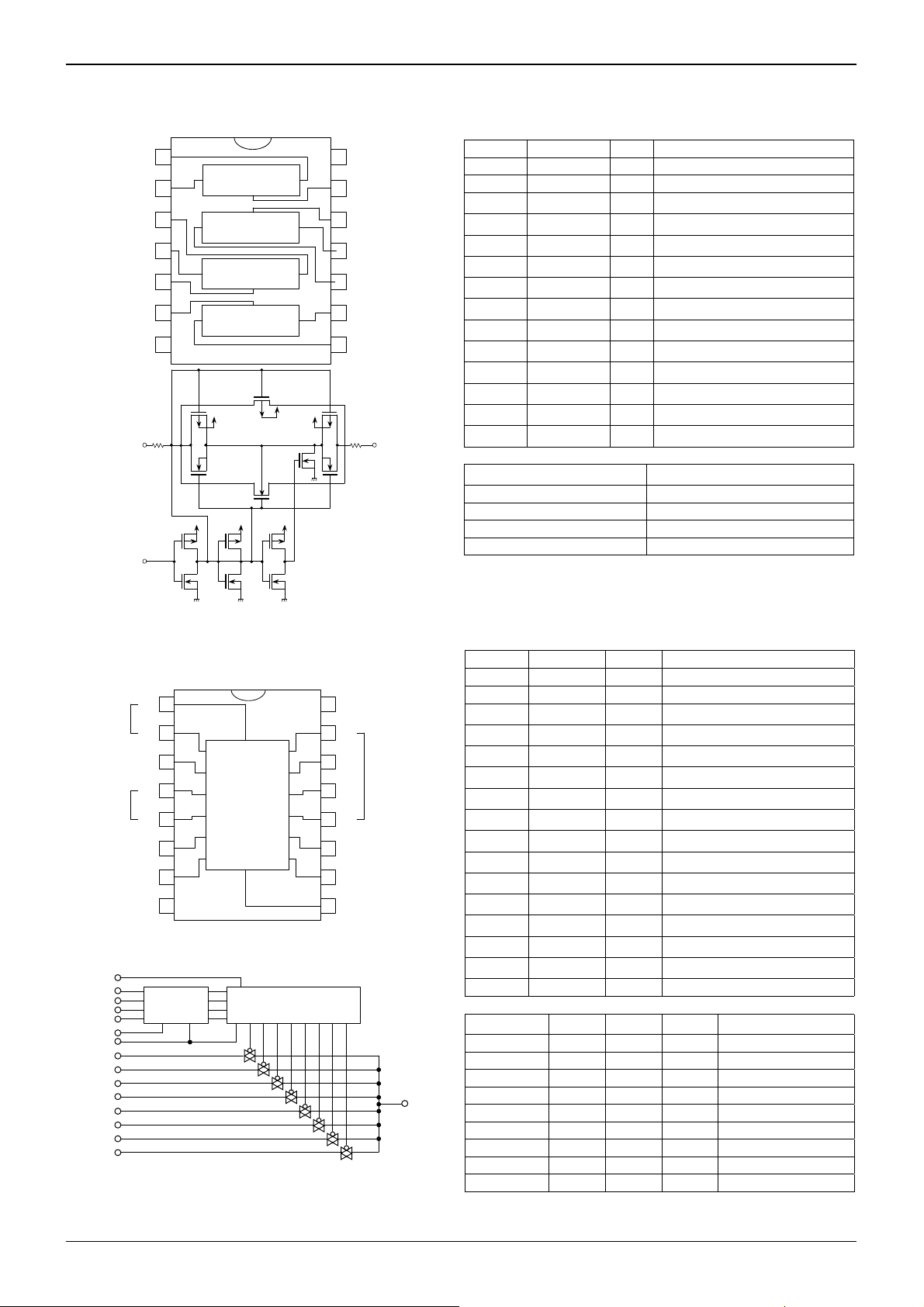
●Pin Configration・Pin Function・Block Diagram ・Truth Table
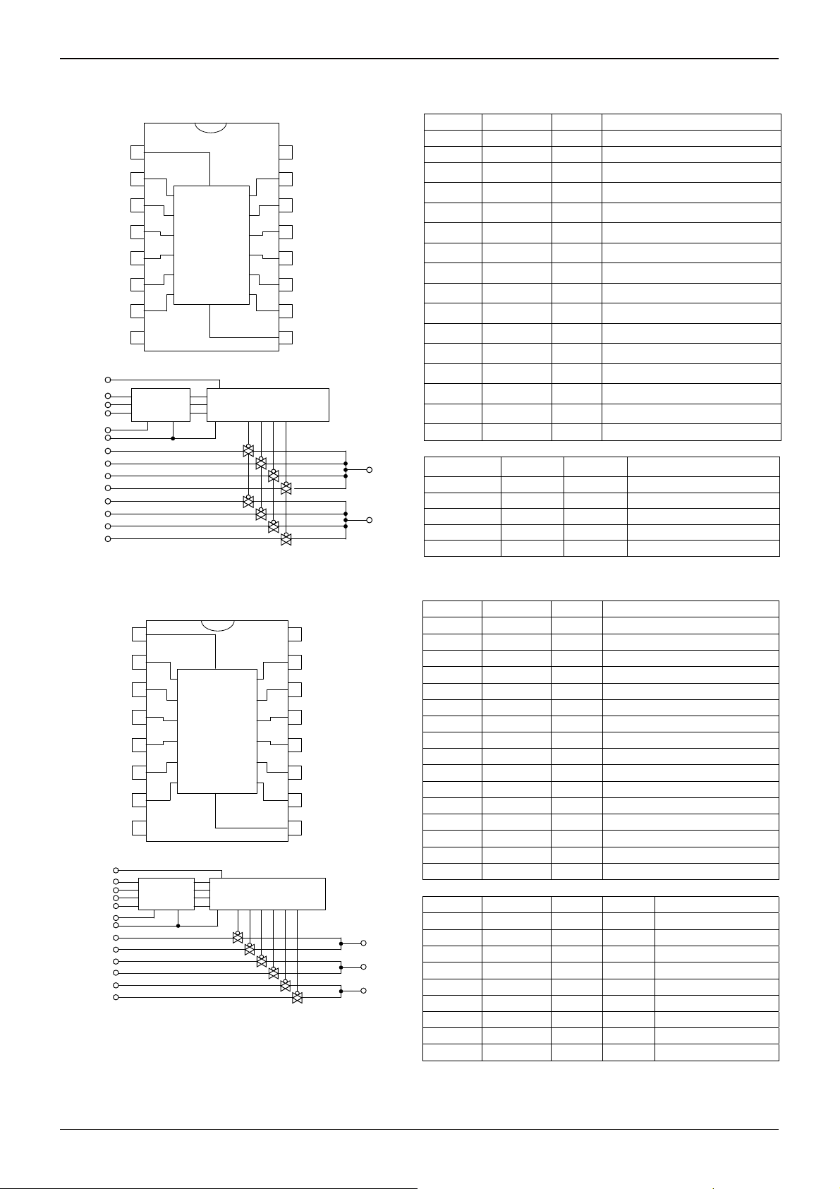
1) BU4066BC Series
PIN FUNCTION
CONT.B
CONT.C
IN/OUT
OUT/IN
OUT/IN
IN/OUT
VEE
IN / OUT
1
2
3
4
5
6
7
OUT/IN IN/OUT
SWA
SWD
OUT/IN IN/OUT
IN/OUT OUT/IN
SWB
SWC
IN/OUT OUT/IN
VDD
VDD VDD
14
VDD
13
CONT.A
12
CONT.D
11
IN/OUT
10
OUT/IN
9
OUT/IN
8
IN/OUT
IN / OUT
PIN No. PIN NAME I/O PIN FUNCTION
1 IN/OUT I/O Analog Switch Input / Output
2 OUT/IN I/O Analog Switch Input / Output
3 OUT/IN I/O Analog Switch Input / Output
4 IN/OUT I/O Analog Switch Input / Output
5 CONT.B I Control Input
6 CONT.C I Control Input
7 VEE - Power Supply(-)
8 IN/OUT I/O Analog Switch Input / Output
9 OUT/IN I/O Analog Switch Input / Output
10 OUT/IN I/O Anal og Switch Input / Output
11 IN/OUT I/O Analog Switch Input / Output
12 CONT.D I Control Input
13 CONT.A I Control Input
14 VDD - Power Supply(+)
TRUTH TABLE
CONTROL ON SWITCH
CONT
A A(1pin-2pin)
B B(3pin-4pin)
C C(8pin-9pin)
D D(10pin-11pin)
2) BU4051BCSeries
PIN FUNCTION
PIN No. PIN NAME I/O PIN FUNCTION
1 X4 I/O Analog Switch Input / Output
2 X6 I/O Analog Switch Input / Output
3 X I/O Analog Switch Input / Output
4 X7 I/O Analog Switch Input / Output
5 X5 I/O Analog Switch Input / Output
6 INHIBIT I Control Input
7 VEE - Power Supply(-)
8 VSS - Power Supply(-)
9 C I Control Input
10 B I Control Input
11 A I Control Input
12 X3 I/O Analog Switch Input / Output
CHANNEL
IN/OUT
COMMON
OUT/IN
INHIBI
X4
X6
X
X7
X5
VEE
VSS
1
2
3
4
5
6
7
8
6
OUT/IN
7
5
INH
VEE
4
C
16
VDD
X2
15
2
14
X1
1
13
0
3
12
11
B
10
CHANNEL
IN/OUT
X0
X3
B
9
C
13 X0 I/O Analog Switch Input / Output
14 X1 I/O Analog Switch Input / Output
VDD
INHIBIT
VSS
VEE
15
A
B
C
X0
X1
X2
X3
X4
X5
X6
X7
LEV EL
CONVERTER
BINARY TO 1 of 8 DECODER
WITH INHIBIT
COMMON
X
16 VDD - Power Supply(+)
TRUTH TABLE
INHIBIT A B C ON SWITCH
L L L L X0
L H L L X1
L L H L X2
L H H L X3
L L L H X4
L H L H X5
L L H H X6
X2 I/O Analog Switch Input / Output
L H H H X7
H X X X NONE
Technical Note
www.rohm.com
© 2011 ROHM Co., Ltd. All rights reserved.
13/17
2011.08 - Rev.B
Page 14
BU4066BC,BU4066BCF,BU4066BCFV,BU4051BC,BU4051BCF,BU4051BCFV,BU4052BC,
A
T
T
BU4052BCF,BU4052BCFV,BU4053BC,BU4053BCF,BU4053BCFV,BU4551B,BU4551BF,BU4551BFV
3) BU4052BC Series
PIN FUNCTION
PIN No. PIN NAME I/O PIN FUNCTION
1 Y0 I/O Analog Switch Input / Output
Y0
Y2
COMMON Y
Y3
Y1
INHIBI
VEE
VSS
1
2
3
4
5
6
7
8 9
2Y
Y OUT/IN
3Y
1Y
INH
VEE
0Y
B
2X
1X
OUT/IN X
OX
3X
A
VDD
16
15
X2
14
X1
COMMON X
13
12
X0
11
X3
10
A
B
2 Y2 I/O Analog Switch Input / Output
3 COMMON Y I/O Analog Switch Input / Output
4 Y3 I/O Analog Switch Input / Output
5 Y1 I/O Analog Switch Input / Output
6 INHIBIT I Control Input
7 VEE - Power Supply(-)
8 VSS - Power Supply(-)
9 B I Control Input
10 A I Control Input
11 X3 I/O Analog Switch Input / Output
12 X0 I/O Anal og Switch Input / Output
13
VDD
INHIBIT
VSS
VEE
A
B
X0
X1
X2
X3
Y0
Y1
Y2
Y3
LEV EL
CONVERTER
BINARY TO 1 of 4 DECODER
WITH INHIBIT
COMMON
X
COMMON
Y
TRUTH TABLE
COMMON X I/O Analog Switch Input / Output
14 X1 I/O Anal og Switch Input / Output
15 X2 I/O Anal og Switch Input / Output
16 VDD - Power Supply(+)
INHIBIT A B ON SWITCH
L L L X0, Y0
L H L X1, Y1
L L H X2, Y2
L H H X3, Y3
H X X NONE
4) BU4053BC Series
PIN FUNCTION
PIN No. PIN NAME I/O PIN FUNCTION
INHIBI
VDD
INHIB IT
VSS
VEE
X0
X1
Y0
Y1
Z0
Z1
1
Y1
2
Y0
3
Z1
4
Z
Z0
5
6
7
VEE
8 9
VSS
A
B
C
LEV EL
CONVERTER
1Y
0Y
1Z
Z
0Z
INH
VEE
C
BINARY TO 1 of 2 DECODER
Y
X
1X
OX
A
B
WITH INHIBIT
VDD
16
15
Y
1
2 Y0 I/O Analog Switch Input / Output
3 Z1 I/O Analog Switch Input / Output
4 Z I/O Analog Switch Input / Output
14
X
13
X1
12
X0
11
10
B
C
5 Z0 I/O Analog Switch Input / Output
6 INHIBIT I Control Input
7 VEE - Power Supply(-)
8 VSS - Power Supply(-)
9 C I Control Input
10 B I Control Input
11 A I Analog Switch Input / Output
12 X0 I/O Analog Switch Input / Output
13 X1 I/O Analog Switch Input / Output
14 X I/O Analog Switch Input / Output
15
16 VDD - Power Supply(+)
TRUTH TABLE
INHIBIT A B C ON SWITCH
COMMON
X
COMMON
Y
COMMON
Z
L L L L X0,Y0,Z0
L H L L X1,Y0,Z0
L L H L X0,Y1,Z0
L H H L X1,Y1,Z0
L L L H X0,Y0,Z1
L H L H X1,Y0,Z1
Y1 I/O Analog Switch Input / Output
Y I/O Analog Switch Input / Output
L L H H X0,Y1,Z1
L H H H X1,Y1,Z1
H X X X NONE
Technical Note
www.rohm.com
© 2011 ROHM Co., Ltd. All rights reserved.
14/17
2011.08 - Rev.B
Page 15

BU4066BC,BU4066BCF,BU4066BCFV,BU4051BC,BU4051BCF,BU4051BCFV,BU4052BC,
W
BU4052BCF,BU4052BCFV,BU4053BC,BU4053BCF,BU4053BCFV,BU4551B,BU4551BF,BU4551BFV
Technical Note
5) BU4551B Series
PIN FUNCTION
W1
1
VDD
16
PIN No. PIN NAME I/O PIN FUNCTION
VDD
CONT
VSS
VEE
W0
W1
X0
X1
Y0
Y1
Z0
Z1
2
X0
3
X1
4
X
5
Y
Y0
6
VEE
7
VSS
8 9
LEV EL
CONVERTER
X0
X1
X
Y
Y0
VEE
1Y
CONT ROL
W0
Z
Z1
Z0
Y1
CONTROL
15
W0
14
W
13
Z
12
Z1
11
Z0
10
Y1
CONTROL
COMMON
W
COMMON
X
COMMON
Y
COMMON
Z
1 W1 I/O Analog Switch Input / Output
2 X0 I/O Analog Switch Input / Output
3 X1 I/O Analog Switch Input / Output
4 X I/O Analog Switch Input / Output
5 Y I/O Analog Switch Input / Output
6 Y0 I/O Control Input
7 VEE - Power Supply(-)
8 VSS - Power Supply(-)
9 CONTROL I Control Input
10 Y1 I/O Control Input
11 Z0 I/O Analog Switch Input / Output
12 Z1 I/O Analog Switch Input / Output
13 Z I/O Analog Switch Input / Output
14 W I/O Analog Switch Input / Output
15 W0 I/O Analog Switch Input / Output
16 VDD - Power Supply(+)
TRUTH TABLE
CONTROL ON SWITCH
0 W0,X0,Y0,Z0
1 W1,X1,Y1,Z1
●Notes for use
1. Absolute maximum ratings
An excess in the absolute maximum ratings, such as supply voltage, temperature range of operating conditions, etc., can
break down the devices, thus making impossible to identify breaking mode, such as short circuit or an open circ uit. If any
over rated values will expect to exceed the absolute maximum ratings, consider adding circuit protection devices, such as
fuses.
2. Connecting the power supply connector backward
Connecting of the power supply in reverse polarity can damage IC. Take precautions when connecting the power supply
lines. An external direction diode can be added.
3. Power Supply lines
Design PCB layout pattern to provide low impedance GND and supply lines. To obtain a low noise ground and supply line,
separate the ground section and supply lines of the digital and analog blocks. Furthermore, for all power terminals to ICs,
connect a capacitor between the power supply and the GND terminal. When applying electrolytic capacitors in the circuit,
not that capacitance characteristic values are reduced at low temperatures.
4. GND voltage
The potential of GND pin must be minimum potential in all operating conditions.
5. Thermal design
Use a thermal design that allows for a sufficient margin in light of the power dissipation (Pd) in actual operating conditions.
6. Inter-pin shorts and mounting errors
Use caution when positioning the IC for mounting on printed circuit boards. The IC may be damaged if there is any
connection error or if pins are shorted together.
7. Actions in strong electromagnetic field
Use caution when using the IC in the presence of a strong electromagnetic field as doin g so may cause the IC to
malfunction.
8. Testing on application boards
When testing the IC on an application board, connecting a capacitor to a pin with low impedance subjects the IC to stress.
Always discharge capacitors after each process or step. Always turn the IC's power supply off before connecting it to or
remove it from a jig or fixture during the inspection process. Ground the IC during assembly steps as an antistatic measure.
Use similar precaution when transporting or storing the IC.
9.Ground Wiring Pattern
When using both small signal and large current GND patterns, it is recommended to isolate the two ground patterns,
placing a signal ground point at the ground potential of application so that the pattern wiring resistance and voltage
variations caused by large currents do not caused by large currents do not cause variations in the small signal ground
voltage. Be careful not to change the GND wiring pattern of any external components, either.
www.rohm.com
© 2011 ROHM Co., Ltd. All rights reserved.
15/17
2011.08 - Rev.B
Page 16

BU4066BC,BU4066BCF,BU4066BCFV,BU4051BC,BU4051BCF,BU4051BCFV,BU4052BC,
BU4052BCF,BU4052BCFV,BU4053BC,BU4053BCF,BU4053BCFV,BU4551B,BU4551BF,BU4551BFV
●Ordering part number
B U 4 5 5 1 B F V - E 2
Technical Note
Part No. Part No.
4066BC
4051BC
4052BC
4053BC
4551B
Package
SOP14
8.7± 0.2
(MAX 9.05 include BURR)
14
8
6.2± 0.3
4.4± 0.2
1
1.5± 0.1
1.27
0.11
0.4± 0.1
7
0.1
0.3MIN
0.15± 0.1
(Unit : mm)
<Tape and Reel information>
Quantity
Direction
of feed
SSOP-B14
6.4 ± 0.3
0.2
±
4.4
14
1
5.0 ± 0.2
8
0.3Min.
7
0.15 ± 0.1
<Tape and Reel information>
Quantity
Direction
of feed
1.15 ± 0.1
0.10
0.65
0.1
0.22 ± 0.1
(Unit : mm)
DIP14
19.4±0.3
14
8
17
6.5±0.3
<Tape and Reel information>
Quantity
Direction of feed
0.51Min.
4.25±0.3
3.2±0.2
2.54
0.5±0.1
7.62
0°−15°
0.3±0.1
(Unit : mm)
Packaging and forming specification
None: DIP14,DIP16
F : SOP14, SOP16
E2: Embossed tape and reel
None:Tray,Tube
FV : SSOP-B14
SSOP-B16
Embossed carrier tapeTape
2500pcs
E2
The direction is the 1pin of product is at the upper left when you hold
()
reel on the left hand and you pull out the tape on the right hand
Reel
Embossed carrier tapeTape
2500pcs
E2
The direction is the 1pin of product is at the upper left when you hold
()
reel on the left hand and you pull out the tape on the right hand
Reel
TubeContainer
1000pcs
Direction of products is fixed in a container tube
1pin
Order quantity needs to be multiple of the minimum quantity.
∗
1pin
Order quantity needs to be multiple of the minimum quantity.
∗
Order quantity needs to be multiple of the minimum quantity.
∗
Direction of feed
Direction of feed
www.rohm.com
© 2011 ROHM Co., Ltd. All rights reserved.
16/17
2011.08 - Rev.B
Page 17

BU4066BC,BU4066BCF,BU4066BCFV,BU4051BC,BU4051BCF,BU4051BCFV,BU4052BC,
BU4052BCF,BU4052BCFV,BU4053BC,BU4053BCF,BU4053BCFV,BU4551B,BU4551BF,BU4551BFV
SOP16
<Tape and Reel information>
10± 0.2
(MAX 10.35 include BURR)
16
9
Quantity
Direction
of feed
4.4± 0.2
6.2± 0.3
1
1.5± 0.1
1.27
0.11
0.4± 0.1
8
0.1
0.3MIN
0.15± 0.1
(Unit : mm)
Embossed carrier tapeTape
2500pcs
E2
The direction is the 1pin of product is at the upper left when you hold
()
reel on the left hand and you pull out the tape on the right hand
Reel
1pin
Order quantity needs to be multiple of the minimum quantity.
∗
SSOP-B16
5.0±0.2
16
4.4±0.2
6.4±0.3
1
9
0.3Min.
8
0.15±0.1
<Tape and Reel information>
Embossed carrier tapeTape
Quantity
Direction
of feed
2500pcs
E2
The direction is the 1pin of product is at the upper left when you hold
()
reel on the left hand and you pull out the tape on the right hand
Technical Note
Direction of feed
DIP16
4.25±0.3
3.2±0.2
1.15±0.1
0.10
0.65
19.4±0.3
16
18
0.51Min.
2.54
0.1
0.22±0.1
9
6.5±0.3
0.5±0.1
7.62
0°−15°
(Unit : mm)
0.3±0.1
(Unit : mm)
Reel
<Tape and Reel information>
TubeContainer
Quantity
Direction of feed
1000pcs
Direction of products is fixed in a container tube
1pin
Order quantity needs to be multiple of the minimum quantity.
∗
Order quantity needs to be multiple of the minimum quantity.
∗
Direction of feed
www.rohm.com
© 2011 ROHM Co., Ltd. All rights reserved.
17/17
2011.08 - Rev.B
Page 18

Notes
No copying or reproduction of this document, in part or in whole, is permitted without the
consent of ROHM Co.,Ltd.
The content specied herein is subject to change for improvement without notice.
The content specied herein is for the purpose of introducing ROHM's products (hereinafter
"Products"). If you wish to use any such Product, please be sure to refer to the specications,
which can be obtained from ROHM upon request.
Examples of application circuits, circuit constants and any other information contained herein
illustrate the standard usage and operations of the Products. The peripheral conditions must
be taken into account when designing circuits for mass production.
Great care was taken in ensuring the accuracy of the information specied in this document.
However, should you incur any damage arising from any inaccuracy or misprint of such
information, ROHM shall bear no responsibility for such damage.
The technical information specied herein is intended only to show the typical functions of and
examples of application circuits for the Products. ROHM does not grant you, explicitly or
implicitly, any license to use or exercise intellectual property or other rights held by ROHM and
other parties. ROHM shall bear no responsibility whatsoever for any dispute arising from the
use of such technical information.
The Products specied in this document are intended to be used with general-use electronic
equipment or devices (such as audio visual equipment, ofce-automation equipment, communication devices, electronic appliances and amusement devices).
The Products specied in this document are not designed to be radiation tolerant.
While ROHM always makes efforts to enhance the quality and reliability of its Products, a
Product may fail or malfunction for a variety of reasons.
Please be sure to implement in your equipment using the Products safety measures to guard
against the possibility of physical injury, re or any other damage caused in the event of the
failure of any Product, such as derating, redundancy, re control and fail-safe designs. ROHM
shall bear no responsibility whatsoever for your use of any Product outside of the prescribed
scope or not in accordance with the instruction manual.
The Products are not designed or manufactured to be used with any equipment, device or
system which requires an extremely high level of reliability the failure or malfunction of which
may result in a direct threat to human life or create a risk of human injury (such as a medical
instrument, transportation equipment, aerospace machinery, nuclear-reactor controller, fuelcontroller or other safety device). ROHM shall bear no responsibility in any way for use of any
of the Products for the above special purposes. If a Product is intended to be used for any
such special purpose, please contact a ROHM sales representative before purchasing.
If you intend to export or ship overseas any Product or technology specied herein that may
be controlled under the Foreign Exchange and the Foreign Trade Law, you will be required to
obtain a license or permit under the Law.
Notice
www.rohm.com
© 2011 ROHM Co., Ltd. All rights reserved.
Thank you for your accessing to ROHM product informations.
More detail product informations and catalogs are available, please contact us.
ROHM Customer Support System
http://www.rohm.com/contact/
R1120
A
 Loading...