

ROHM BU38803, BU38703, BU38603 Datasheet

1
Video ICs
System control servo
BU38603 / BU38703 / BU38803
The BU38603, BU38703 and BU38803 are servo controller ICs for VCRs. They contain a high-speed, 8-bit CPU and
perform the processing required for the drum, capstan, FV and PV completely in software, allowing a large reduction
in the number of external components required. They also contain high-performance linear amplifiers, eliminating the
need for interface ICs. Specialized hardware is included for items that require high-speed processing, to allow
efficient utilization of the CPU.
•
Applications
VHS VCRs and camcorders
•
Features
1) CPU
499 commands (69 types)
Memory-mapped I / O
Minimum command execution time: 250ns (8MHz)
2)ROM capacity
BU38603: 16384 × 8 bit
BU38703: 24576 × 8 bit
BU38803: 32768 × 8 bit
3) RAM capacity: 512 × 8bit
4) Interrupt
Pattern generator: 1
Watch-dog timer: 1
External interrupts: 1
FG interrupts: 5
Internal interrupts: 7
Two timers, serial transmission, interrupt, VHSW,
CTL interval timer (fixed) / VISS
∗ Multi-layer interrupts possible.
5) Free-running counter: 19 bit
6) PWM output: 12 bit × 2
7) Pattern generator
17 bits from FRC MSB used.
Output
Internal: 3 bit
External (PO): 5 bit
External (PIO): 6 bit
8) Programmable pre-scaler
CFG: 7 bit
CTL: 6 bit
9) Head amplifier / chroma rotary
Generated from pattern generator output.
10) Built-in AGC. Five-bits used to switch the gain
control registers for the CTL amplifier.
11) CTL counter: 1 / 30 or 1 / 25
12) Data shift PLL calculation: 24 bit
13) Timer: 8 bit × 2
14) Synchronous serial input/output: 8 bit × 1
15) VH PULSE
V separeted from composite synchronous snal.
Pseudo V generated from pattern generator
output.
Superimposed pseudo H synchronized with
the composite synchronous signal.
16) VISS / VASS
VASS 0 / 1 discrimination
VISS discrimination threshold: 3
Aspect discrimination.
D / A CTL switching.
17) Standard I / O
Parallel I / O (PIO): 32 bit
Parallel output (PO): 6 bit
18) A / D converter: 8 bits × 8 channels
Can be masked-programmed to be parallel inputs.
19) Watch-dog timer
Setting period: 4
20) Linear circuits
DFG: amplifier / comparator
CFG: amplifier / comparator
CTL: differential amplifier / comparator
DPG: comparator
2
Video ICs BU38603 / BU38703 / BU38803
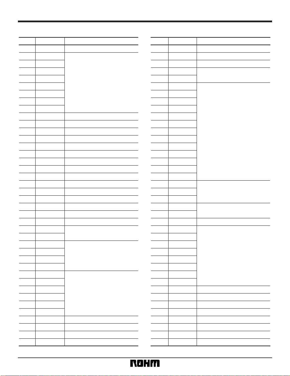
•
Block diagram
CPU
PWM
PTG
VH PULSE
FRC
VISSVASS
ROM / RAM
PI / O
SI / O
PO0-PO5
P1-P31
P0
SI
SO
SCK
ADC0-ADC7
COUNTP
PBCTL
Vref
PWM0
PWM1
VHSW
AHSW
HAMPSW
CHROT
ENVIN
FV
CSYNC
RESETB
CTL + DFGIN DFGOUT DPGIN CFGIN CFGOUTCTLAMPOUTCTL – CTLAMP –
(P0)
Timer
Data bus
Interrupts
Watchdog
A / D converter
Data shift
Linear time counter
Head amp,
chroma
Servo mode register
CFG,
CTL division
Gain control
Linear
•
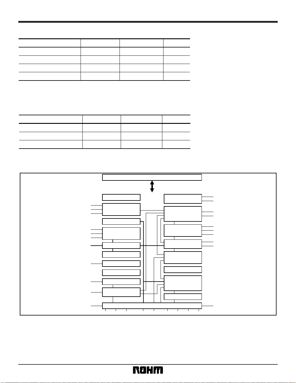
Absolute maximum ratings (Ta = 25°C)
Parameter
Limits
Unit
V
DD, VDDA, VDAD
V
V
IN
VSS – 0.3 ~ VDD + 0.3
V
mW
°C
Symbol
Pd
Tstg
500
∗
1
0.3 ~ 7.0
∗
2
– 55 ~ + 125
∗
1 Reduced by 5mW for each increase in Ta of 1°C over 25°C.
∗
2 Use with VSS = VSSA = VSAD, and VDD = VDDA = VDAD.
Applied voltage
Pin applied voltage
Power dissipation
Storage temperature range
•
Recommended operating conditions
Parameter
Symbol
Limits
Unit
V
DD, VDDA, VDDB
4.5 ~ 5.5
V
F
CK
8
MHz
°CTopr
– 25 ~ + 75
Power supply voltage
Clock frequency
Operating temperature
3
Video ICs BU38603 / BU38703 / BU38803
•
Pin descriptions
1 VSAD
2 ADC0
3 ADC1
4 ADC2
5 ADC3
6 ADC4
7 ADC5
8 ADC6
9 ADC7
10 VDAD
11 DFGOUT
12 DFGIN
13 DPGIN
14 CFGIN
15 CFGOUT
16 VSSA
17 V
ref
18 CTLAMP –
19 CTLAMPOUT
20 CTL –
21 CTL +
22 VDDA
23 RESETB
24 TEST
25 PO5
26 PO4
27 P31
28 P30
29 P29
30 P28
31 P27
32 P26
33 P25
34 P24
35 P23
36 P22
37 PO3
38 VHSW
39 AHSW
40 HAMPSW
41 CHROT
42 FV
43 V
DD
44 PWM0
45 PWM1
46 P21
47 P20
48 P19
49 P18
50 P17
51 P16
52 P15
53 P14
54 P13
55 P12
56 P11
57 P10
58
59 PO2
60 PO1
61 PO0
62 CLOCKO
63 CLOCKI
64 V
SS
65 P8
66 P7
67 P6
68 P5
69 P4
70 P3
71 P2
72 P1
73 P0
74 SI
75 SO
76 SCK
77 ENVIN
78 CSYNC
79 COUNTP
80 PBCTL
P9
Pin name Function
Pin namePin No.
Pin No.Function
A / D convertor circuit GND.
Can be optionally mask – programmed
to be either A / D or parallel inputs.
A / D convertor circuit power supply.
Drum FG amplifier output
Drum FG amplifier input
Drum PG comparator input
Capstan FG amplifier input
Capstan FG amplifier output
Linear circuit GND
Internal BIAS and power-on reset pin
CTL amplifier – input
CTL amplifier output
CTL coil – connection
CTL coil + connection
Linear circuit power supply
Power supply reset
Test mode input (normally GND)
Parallel output
Parallel I / O
Parallel I / O and pattern generator
output
Chroma rotary switch output
Pseudo Vsync output
Logic circuit power supply
PWM output
Parallel I / O
Parallel output
For connection of oscillator
Logic circuit GND
Parallel I / O
Parallel I / O and external interrupt
Serial I / O data input
Serial I / O data I / O
Serial I / O clock I / O
Envelope detector logic input
Composite signal logic input
CTL counter pulse output
CTL logic output
Parallel output and pattern generator output
Head amplifier switch output
Pattern generator AHSW output
Pattern generator VHSW output
 Loading...