

Page 1
CMOS LDO Regulators for Portable Equipments
1ch 200mA
CMOS LDO Regulators
BU□□TD2WNVX series
●Description
BUTD2WNVX series is high-performance FULL CMOS regulator with 200-mA output, which is mounted on micro
miniature package SSON004X1010 (1.0 mm 1.0 mm 0.6 mm). It has excellent noise characteristics and load
responsiveness characteristics despite its low circuit current consumption of 35µA. It is most appropriate for various
applications such as power supplies for logic IC, RF, and camera modules. Micro miniature SSON004X1010 with built-in
heatsink is adopted for the package, which contributes to the space-saving design of the set.
●Features
1) High-accuracy output voltage of 1% (25 mV on Vout<2.5V products)
2) High ripple rejection: 70 dB (Typ., 1 kHz,)
3) Compatible with small ceramic capacitor (CIN=Co=0.47 µF)
4) Low current consumption: 35 µA
5) ON/OFF control of output voltage
6) With built-in overcurrent protection circuit and thermal shutdown circuit
7) With built-in output discharge circuit
8) Adopting ultra-small package SSON004X1010
●Applications
Battery-powered portable equipment, etc.
●Line up
■200 mA BU□□TD2WNVX Series
Product Name 1.0 1.2 1.5 1.8 1.85 1.9 2.0 2.05 2.1 2.3 2.5 Package
No.11020ECT07
BU□□TD2WNVX
Model name:BU□□
Symbol
a
○ ○ ○ ○ ○ ○ ○ ○ ○ ○ ○
SSON004X1010 2.6 2.7 2.8 2.85 2.9 3.0 3.1 3.2 3.3 3.4
○ ○ ○ ○ ○ ○ ○ ○ ○ ○
TD2WNVX
a
Contents
Specification of output voltage
□□
10 1.0 V(Typ.) 20 2.0 V(Typ.) 27 2.7 V(Typ.) 32 3.2 V(Typ.)
12 1.2 V(Typ.) 2A 2.05 V(Typ.) 28 2.8 V(Typ.) 33 3.3 V(Typ.)
15 1.5 V(Typ.) 21 2.1 V(Typ.) 2J 2.85 V(Typ.) 34 3.4 V(Typ.)
18 1.8 V(Typ.) 23 2.3V(Typ.) 29 2.9 V(Typ.)
1J 1.85 V(Typ.) 25 2.5 V(Typ.) 30 3.0 V(Typ.)
19 1.9 V(Typ.) 26 2.6 V(Typ.) 31 3.1 V(Typ.)
Output voltage
(V)
□□
Output voltage
(V)
□□
Output voltage
(V)
□□
Output voltage
(V)
www.rohm.com
© 2011 ROHM Co., Ltd. All rights reserved.
1/41
2011.07 - Rev.C
Page 2
BU□□TD2WNVX series
●Absolute maximum ratings
Parameter Symbol Ratings Unit
Maximum applied power voltage VMAX -0.3 ~ +6.5 V
Technical Note
Power dissipation Pd 560
(*1)
mW
Maximum junction temperature TjMAX +125 ℃
Operational temperature range Topr -40 ~ +85 ℃
Storage temperature range Tstg -55 ~ +125 ℃
(*1) When PCB (70 mm 70 mm, thickness 1.6-mm glass epoxy) a standard ROHM board is implemented.
Reduced to 5.6 mW/℃ when used at Ta=25℃ or higher.
●Recommended operating range (Do not exceed Pd.)
Parameter Symbol Ratings Unit
Input power supply voltage VIN 1.7 ~ 5.5 V
Maximum output current IMAX 200 mA
●Recommended operating conditions
Parameter Symbol
Ratings
Min. Typ. Max.
Unit Conditions
Input capacitor CIN 0.22
Output capacitor CO 0.22
(*2) Set the capacity value of the capacitor so that it does not fall below the minimum value, taking temperature characteristics,
DC device characteristics, and change with time into consideration.
(*2)
0.47 - µF A ceramic capacitor is recommended.
(*2)
0.47 - µF A ceramic capacitor is recommended.
www.rohm.com
© 2011 ROHM Co., Ltd. All rights reserved.
2/41
2011.07 - Rev.C
Page 3

BU□□TD2WNVX series
Technical Note
●Electrical characteristics(Ta=25℃, VIN=VOUT+1.0V
Parameter Symbol
(*3)
, STBY=VIN, CIN=0.47μF, CO=0.47μF, unless otherwise noted.)
Limits
Min. Typ. Max.
Unit Conditions
Overall Device
Output Voltage VOUT
VOUT
×0.99
VOUT
-25mV
VOUT
VOUT
×1.01
VOUT
+25mV
IOUT=10µA,VOUT≧2.5V
V
IOUT=10µA,VOUT<2.5V
Operating Current IIN - 35 60 µA IOUT=0mA
Operating Current (STBY) ISTBY - - 1.0 µA STBY=0V
Ripple Rejection Ratio RR 45 70 - dB VRR=-20dBv,fRR=1kHz,IOUT=10mA
- 280 540 mV
- 260 500 mV
Dropout Voltage VSAT
- 240 460 mV
- 220 420 mV
Line Regulation VDL - 2 20 mV
2.5V≦VOUT≦2.6V
(VIN=0.98*VOUT,IOUT=200mA)
2.7V≦VOUT≦2.85V
(VIN=0.98*VOUT,IOUT=200mA)
2.9V≦VOUT≦3.1V
(VIN=0.98*VOUT,IOUT=200mA)
3.2V≦VOUT≦3.4V
(VIN=0.98*VOUT,IOUT=200mA)
VIN=VOUT+1.0V to 5.5V
IOUT=10µA
(*4)
Load Regulation VDLO - 10 80 mV IOUT=0.01mA to 100mA
Over-current Protection (OCP)
Limit Current ILMAX 220 400 700 mA Vo=VOUT*0.95
Short Current ISHORT 20 70 150 mA Vo=0V
Standby Block
Discharge Resistor RDSC 20 50 80 Ω VIN=4.0V, STBY=0V, VOUT=4.0V
STBY Pin Pull-down Current ISTB 0.1 0.6 2.0 µA STBY=1.5V
ON VSTBH 1.2 - 5.5 V
STBY Control Voltage
OFF VSTBL -0.3 - 0.3 V
* This product does not have radiation-proof design.
(*3) VIN=2.5V for VOUT≦1.5V
(*4) VIN=2.5V to 5.5V for VOUT≦1.5V
●Electrical characteristics
(Ta=25℃, STBY=VIN, CIN=0.47μF, Co=0.47μF, unless otherwise noted.)
Parameter Symbol
of each Output Voltage
Limits
Min. Typ. Max.
80 160 -
Unit Conditions
VIN=1.7V
1.2V
200 - - VIN=2.1V
1.5V
Maximum
output current
1.8V 200 - - VIN=2.4V
1.9V 200 - - VIN=2.5V
www.rohm.com
© 2011 ROHM Co., Ltd. All rights reserved.
60 120 - VIN=1.8V
mA
200 - - VIN=2.2V
3/41
2011.07 - Rev.C
Page 4
BU□□TD2WNVX series
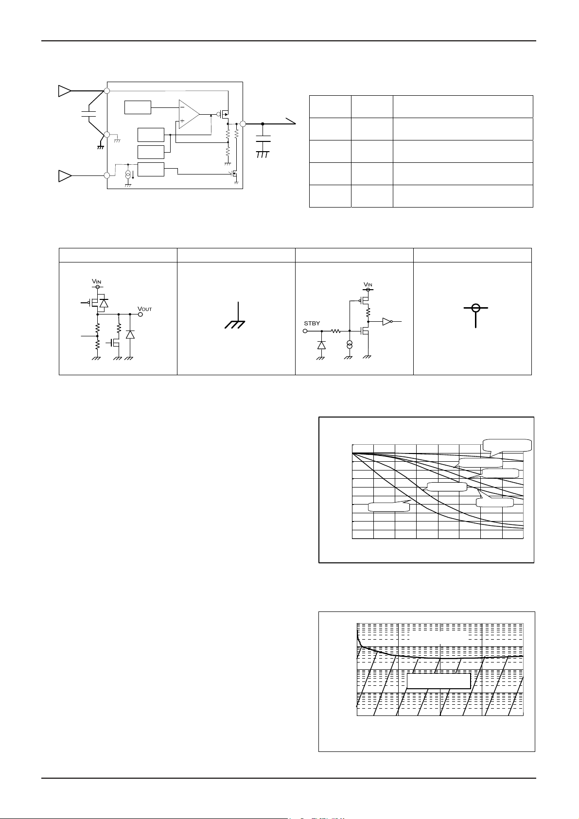
●Block diagram, recommended circuit diagram, and pin configuration diagram
BU□□TD2WNVX
VIN
Cin
VSTBY
VIN
4
VREF
2
GND
STBY
3
Recommended ceramic capacitor for Cin & Co
Murata Manufacturing Co., Ltd.
GRM188B11A474KA61D
OCP
TSD
STBY
Fig.1 Recommended circuit diagram
Discharge
VOUT
1
VOUT
Co
PIN No. Symbol Function
1 VOUT
2 GND
3 STBY
4 VIN
●Input / Output terminal equivalent circuit schematic
1pin (VOUT) 2pin (GND) 3pin (STBY) 4pin (VIN)
Technical Note
Voltage output
Grounding
ON/OFF control of output voltage
(High: ON, Low: OFF)
Power input
Fig.2 Input/Output equivalent circuit
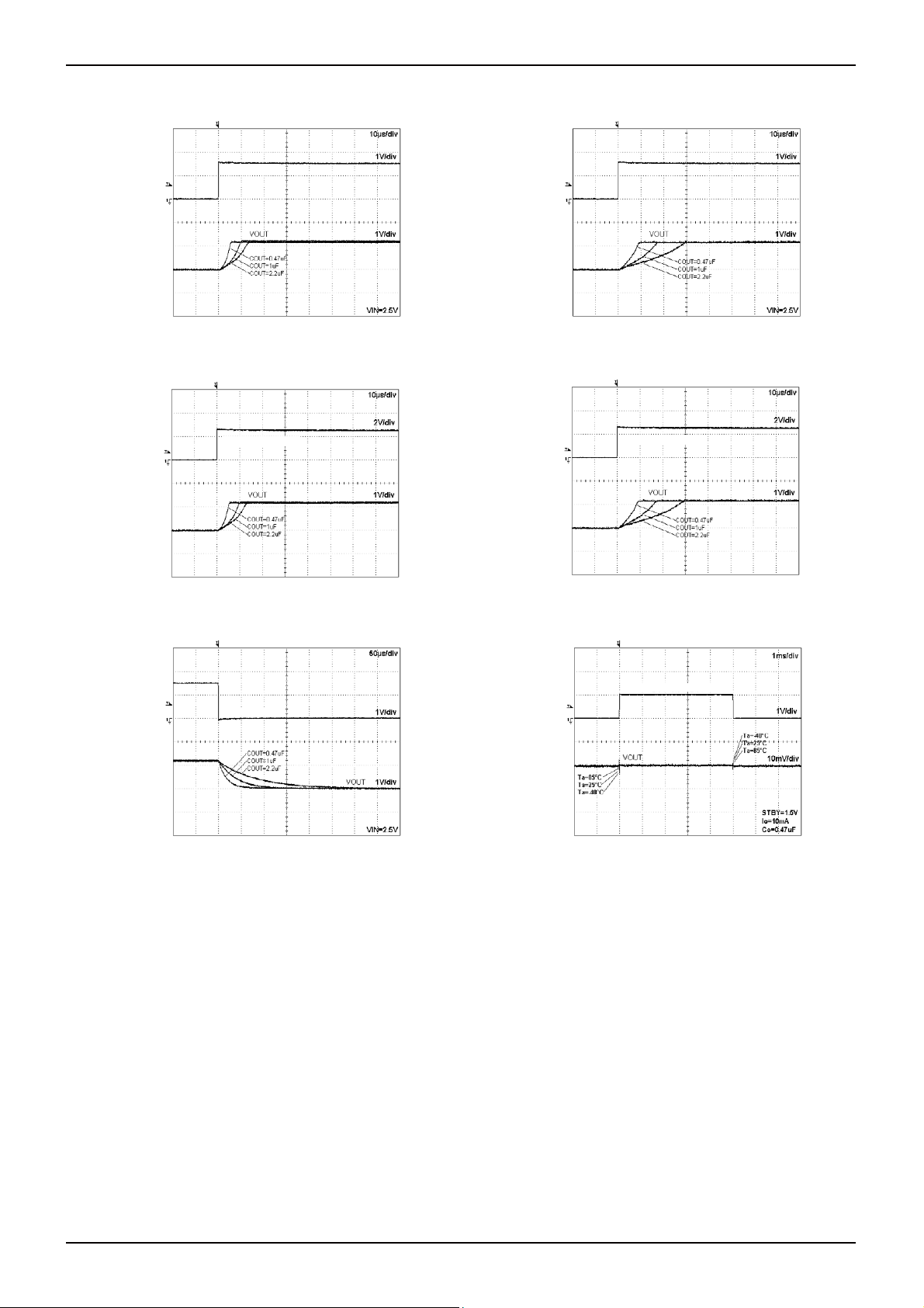
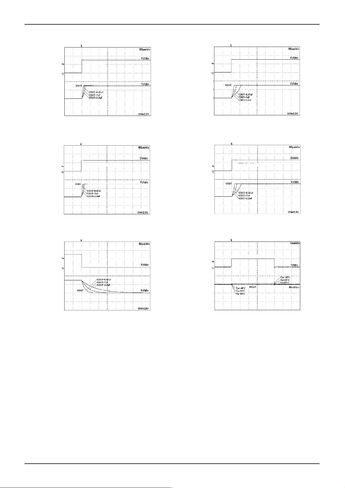
●About input/output capacitor
It is recommended to place a capacitor as close as possible to
the pins between the input terminal and GND or between the
output terminal and GND.
The capacitor between the input terminal and GND becomes
valid when source impedance increases or when wiring is long.
The larger the capacity of the output capacitor between the
output terminal and GND is, the better the stability and
characteristics in output load fluctuation become.
However, please check the status of actual implementation.
Ceramic capacitors generally have variation, temperature
characteristics, and direct current bias characteristics and the
capacity value also decreases with time depending on the
usage conditions. It is recommended to select a ceramic
capacitor upon inquiring about detailed data of the related
manufacturer.
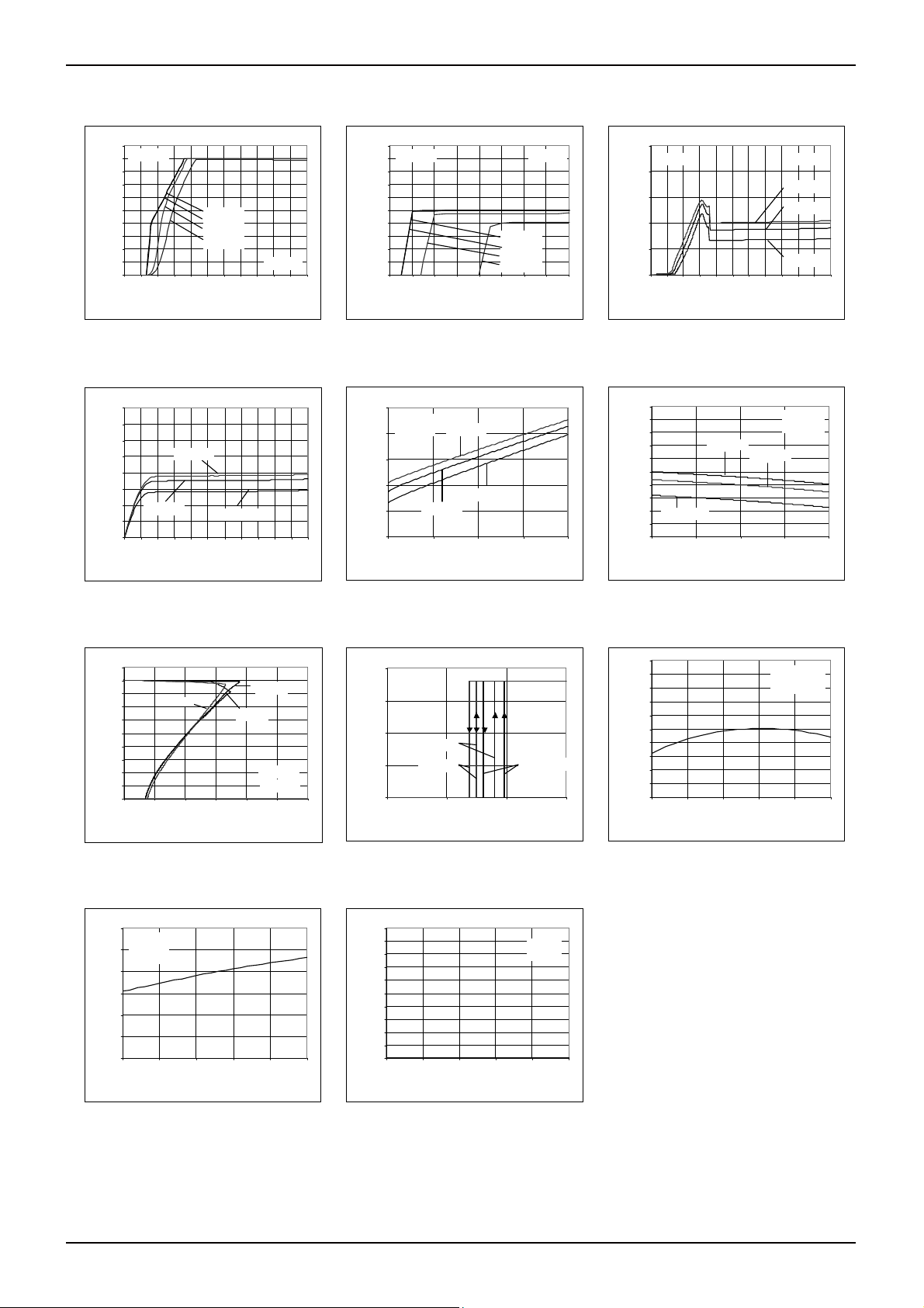
●About the equivalent series resistance (ESR) of a ceramic capacitor
Capacitors generally have ESR (equivalent series resistance)
and it operates stably in the ESR-IOUT area shown on the right.
Since ceramic capacitors, tantalum capacitors, electrolytic
capacitors, etc. generally have different ESR, please check the
ESR of the capacitor to be used and use it within the stability
area range shown in the right graph for evaluation of the actual
application.
Capacity value of ceramic capacitor - DC bias characteristics
10
0
-10
-20
-30
-40
-50
-60
-70
Capacitance Change [%]
-80
-90
-100
10-V wit hstand voltag e
F char acter isti cs
00.511.522.533.54
Example
(
)
10-V withstand voltag e
F char acteri sti cs
DC Bias Voltage [V]
10-V wit hstand volt age
B charac teri stic s
4-V withstand voltag e
X6S characteristics
Fig.3 Capacity – bias characteristics
Cout=0.47μF ,CIN=0.47μF ,Temp=+25℃
100
Unstable region
10
1
ESR [Ω]
ESR [Ω]
0.1
Stable region
0.01
0 50 100 150 200
IOUT [mA ]
Fig.4 Stability area characteristics (Example)
10-V withstand voltag e
B1charac teri sti cs
GRM18 8B11A105KA61D
6.3-V wi thstand volta ge
B charac teri stic s
www.rohm.com
© 2011 ROHM Co., Ltd. All rights reserved.
4/41
2011.07 - Rev.C
Page 5
BU□□TD2WNVX series
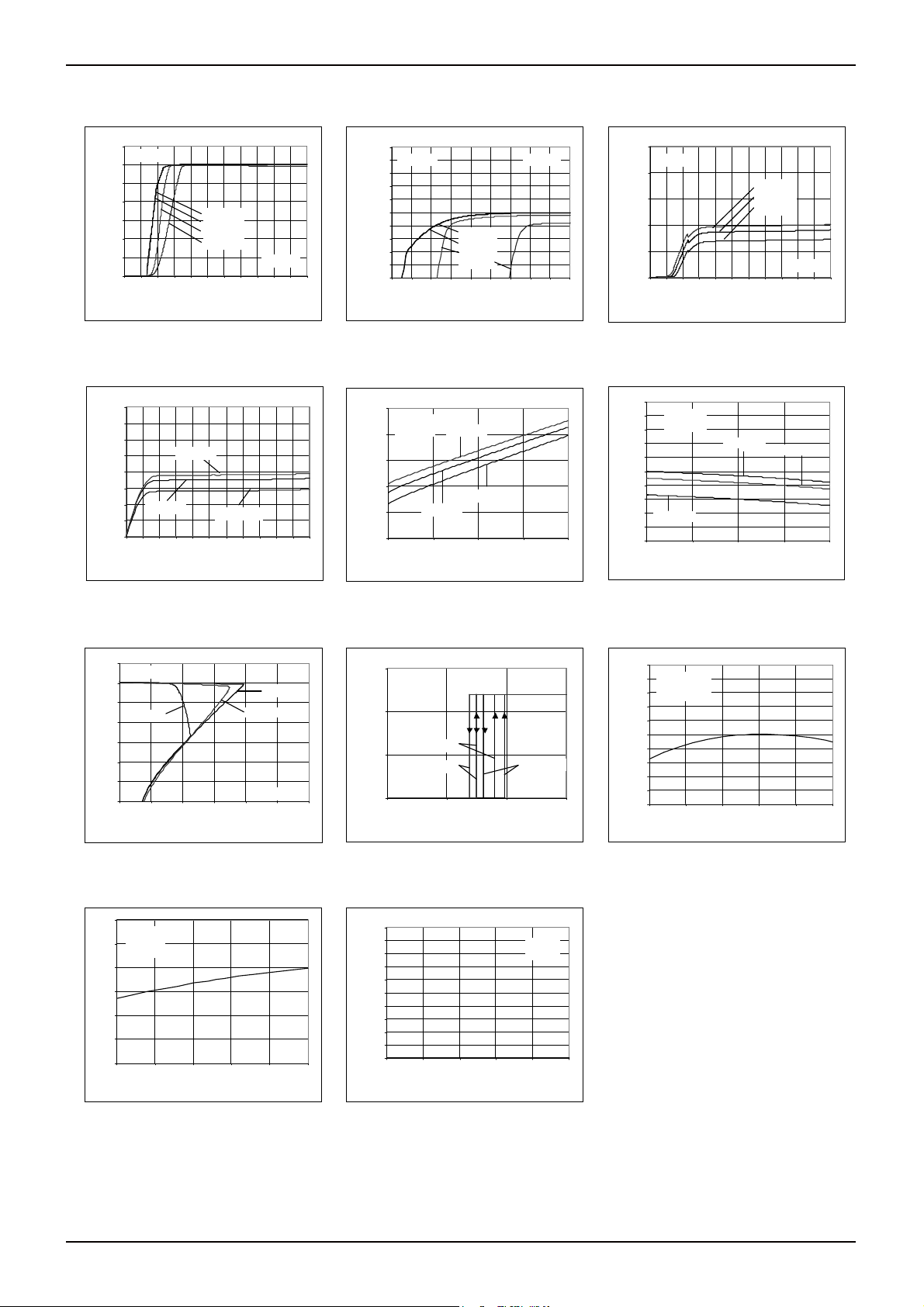
●Reference data BU12TD2WNVX (Ta=25℃ unless otherwise specified.)
1.4
Temp=25°C
1.2
1.0
0.8
0.6
0.4
Output Voltage (V)
0.2
0.0
00.511.522.533.544.555.5
Io=0uA
Io=1 00uA
Io=50mA
Io=200mA
Input Voltage (V)
VIN= STBY
1.25
Temp=25°C
1.24
1.23
1.22
1.21
1.20
1.19
1.18
Output Voltage (V)
1.17
1.16
1.15
1.1 1.2 1.3 1.4 1.5 1.6 1.7 1.8 1.9 2
Io=0uA
Io=1 00uA
Io=50mA
Io=200mA
Input Voltage (V)
Fig.5. Output Voltage
Fig.6. Line Regulation
1.6
1.4
1.2
1.0
0.8
0.6
0.4
STBY Pin Cu rr ent ( uA)
0.2
0.0
00.511.522.5 33.544.555.5
Temp=25°C
Temp=85°C
Temp= -40°C
Input Voltage (V)
100
VIN= 2.5V
STBY= 1.5V
80
60
40
Gnd Curr ent (uA)
20
0
0 0.05 0.1 0.15 0.2
Temp=85°C
Temp=-40°C
Temp=25°C
Output Current (A)
Fig.8. VSTBY - ISTBY
Fig.9. IOUT - IGND Fig.10. Load Regulation
1.4
Temp=25°C
1.2
1.0
VIN=1.7V
0.8
0.6
0.4
Output Voltage (V)
0.2
0.0
0 0.1 0.2 0.3 0.4 0.5 0.6
VIN=5.5V
Output Current (A)
VIN=2.5V
STBY= 1.5V
1.5
VIN= 2.5V
Io=0mA
1.0
0.5
Output Voltage (V)
0.0
Temp=25°C
Temp=85°C
00.511.5
STBY V oltage (V )
Fig.11. OCP Threshold
Fig.12. STBY Threshold
60
VIN =2.5V
STBY=1.5V
50
Io=0mA
40
30
20
Gnd Cur rent (uA)
10
0
-40 -15 10 35 60 85
Temp ( °C)
1.0
0.9
0.8
0.7
0.6
0.5
0.4
0.3
Gnd Curr ent (uA)
0.2
0.1
0.0
-40 -15 10 35 60 85
Temp ( °C)
Fig.14. IGND vs Temp Fig.15. IGND - Temp (STBY)
VIN= STBY
Temp=-40°C
VIN= 2.5V
STBY=0V
Technical Note
100
Io=0uA
80
60
40
Gnd Current (uA)
20
0
00.511.522.533.544.555.5
Input Voltage (V )
Fig.7. Circuit Current IGND
1.25
VIN= 2.5V
1.24
STBY=1.5V
1.23
1.22
1.21
1.20
1.19
1.18
Output Voltage ( V)
1.17
Temp=-40°C
1.16
1.15
0 0. 05 0.1 0.15 0.2
Output Current (A)
1.25
VIN= 2.5V
1.24
STBY=1.5V
1.23
Io=0.1mA
1.22
1.21
1.20
1.19
1.18
Output Voltage (V)
1.17
1.16
1.15
-40 -15 10 35 60 85
Fig.13. VOUT - Temp
Temp=25°C
Temp ( °C)
Temp=85°
Temp=25°C
Temp=-40°C
VIN= STBY
Temp= 85°C
www.rohm.com
© 2011 ROHM Co., Ltd. All rights reserved.
5/41
2011.07 - Rev.C
Page 6
BU□□TD2WNVX series
p
g
(
)
p
(
)
p
g
(
)
p
(
)
●Reference data BU12TD2WNVX (Ta=25 ℃unless otherwise specified.)
IOUT=0mA→50mA
V
e
ut Volta
Out
1.25
1.20
1.15
1.10
Output Current (mA)
100
50
0
Fig.16. Load Response
IOUT=0mA→100mA
1.25
1.20
1.15
Output Voltage (V)
1.10
Output Current (mA)
100
50
0
Fig.18. Load Response
IOUT=0mA→200mA
1.30
1.20
1.10
Output Voltage (V)
1.00
Output Current (mA)
200
100
0
Fig.20. Load Response
IOUT=50mA→100mA
1.25
1.20
1.15
Output Voltage (V)
1.10
Output Current (mA)
100
50
0
Technical Note
IOUT=50mA→0mA
1.30
1.25
1.20
Output Voltage (V)
1.15
Fig.17. Load Response
IOUT=100mA→0mA
1.30
1.25
1.20
Output Voltage (V)
1.15
Fig.19. Load Response
IOUT=200mA→0mA
1.40
1.30
1.20
Output Voltage (V)
1.10
Fig.21. Load Response
IOUT=100mA→50mA
1.25
V
e
1.20
1.15
ut Volta
Out
1.10
Out
100
ut Current
50
mA
0
Output Current (mA)
100
50
0
Output Current (mA)
200
100
0
Out
ut Current
100
50
mA
0
Fig.22. Load Response
www.rohm.com
© 2011 ROHM Co., Ltd. All rights reserved.
6/41
Fig.23. Load Response
2011.07 - Rev.C
Page 7
BU□□TD2WNVX series
●Reference data BU12TD2WNVX (Ta=25℃ unless otherwise specified.)
STBY=0→1.5V
2.0
1.0
0.0
Output Voltage (V)
STBY Voltage (V)
2.0
1.0
0.0
Fig.24. Start Up Time
Iout=0mA
VIN=STBY=0→2.5V
2.0
1.0
0.0
Output Voltage (V)
STBY Voltage (V)
4.0
2.0
0.0
Fig.26. Start Up Time
(VIN=STBY) Iout=0mA
STBY=1.5→0V
2.0
1.0
0.0
Output Voltage (V)
STBY Voltage (V)
2.0
1.0
0.0
Fig.28. Discharge Time
Technical Note
STBY=0→1.5V
2.0
1.0
0.0
Output Voltage (V)
Fig.25. Start Up Time
Iout=200mA
VIN=STBY=0→2.5V
2.0
1.0
0.0
Output Voltage (V)
Fig.27. Start Up Time
(VIN=STBY) Iout=200mA
VIN=2.5V→3.5V→2.5V
1.21
1.20
1.19
Output Voltage (V)
1.18
Fig.29. VIN Response
STBY Voltage (V)
2.0
1.0
0.0
STBY Voltage (V)
4.0
2.0
0.0
Input Voltage (V)
4.5
3.5
2.5
www.rohm.com
© 2011 ROHM Co., Ltd. All rights reserved.
7/41
2011.07 - Rev.C
Page 8
BU□□TD2WNVX series
●Reference data BU15TD2WNVX (Ta=25℃ unless otherwise specified.)
2.0
Temp=25°C
1.8
1.6
1.4
1.2
1.0
0.8
0.6
Output Voltage (V)
0.4
0.2
0.0
00.511.522.533.544.555.5
Io=0uA
Io=100uA
Io=50mA
Io=200mA
Input Voltage (V)
1.55
Temp=25°C
1.54
1.53
1.52
1.51
1.50
1.49
1.48
Output Voltage (V)
1.47
1.46
1.45
1.41.51.61.71.81.9 2 2.1
Io=0uA
Io=1 00uA
Io=50mA
Io=200mA
Input Voltage (V )
Fig.30. Output Voltage
Fig.31. Line Regulation
1.6
1.4
1.2
1.0
0.8
0.6
0.4
STBY Pin Curr ent ( uA)
0.2
0.0
00.511.522.5 33.544.555.5
Temp=25°C
Temp=85°C
Temp= -40°C
Input Voltage (V)
100
VIN= 2.5V
STBY= 1.5V
80
60
40
Gnd Curr ent (uA)
20
0
0 0.05 0.1 0.15 0.2
Temp=85°C
Temp=-40°C
Temp=25°C
Output Current (A )
Fig.33. VSTBY - ISTBY
Fig.34. IOUT - IGND
2.0
Temp=25°C
1.8
1.6
1.4
Output Voltage (V)
VIN=2.0V
1.2
1.0
0.8
0.6
0.4
0.2
0.0
0 0.10.20.30.40.50.6
Output Current (A )
VIN=2.5V
VIN=5.5V
STBY=1.5V
2.0
VIN= 3.8V
Io=0mA
1.5
1.0
0.5
Output Voltage (V)
0.0
Temp=25°C
Temp=85°C
00.511.5
STBY V oltage (V)
Fig.36. OCP Threshold
Fig.37. STBY Threshold Fig.38. VOUT - Temp
60
VIN= 2.5V
STBY=1.5V
50
Io=0mA
40
30
20
Gnd Current (uA)
10
0
-40 -15 10 35 60 85
Temp ( °C)
1.0
0.9
0.8
0.7
0.6
0.5
0.4
0.3
Gnd Curr ent (uA)
0.2
0.1
0.0
-40 -15 10 35 60 85
Temp ( °C)
Fig.39. IGND vs Temp
Fig.40. IGND vs Temp (STBY)
VIN= STBY
Temp=-40°C
VIN= 2.5V
STBY=0V
Technical Note
100
IO=0uA VIN= STBY
80
60
40
Gnd Curr ent (uA)
20
0
00.511.522.533.544.555.5
Fig.32. Circuit Current IGND
1.55
1.54
1.53
1.52
1.51
1.50
1.49
1.48
Output Voltage (V)
1.47
1.46
1.45
0 0.05 0.1 0.15 0.2
Fig.35. Load Regulation
1.55
1.54
1.53
1.52
1.51
1.50
1.49
1.48
Output Voltage (V)
1.47
1.46
1.45
-40 -15 10 35 60 85
VIN= 2.5V
STBY=1.5V
Temp=-40°C
VIN= 2.5V
STBY=1.5V
Io=0.1mA
Input Voltage (V)
Temp=25°C
Temp=85°C
Output Current (A)
Temp ( °C)
Temp= 85°C
Temp= 25°C
Temp= -40°C
www.rohm.com
© 2011 ROHM Co., Ltd. All rights reserved.
8/41
2011.07 - Rev.C
Page 9
BU□□TD2WNVX series
p
g
(
)
p
g
(
)
p
g
(
)
p
g
(
)
p
g
(
)
p
g
(
)
p
g
(
)
p
g
(
)
●Reference data BU15TD2WNVX (Ta=25℃ unless otherwise specified.)
V
e
ut Volta
Out
1.55
1.50
1.45
1.40
IOUT=0mA→50mA
Output Current (mA)
100
50
0
Fig.41. Load Response
IOUT=0mA→100mA
1.55
V
e
1.50
1.45
ut Volta
Out
1.40
Output Current (mA)
100
50
0
Fig.43. Load Response
IOUT=0mA→200mA
V
e
ut Volta
Out
1.60
1.50
1.40
1.30
Output Current (mA)
200
100
0
Fig.45. Load Response
IOUT=50mA→100mA
V
e
ut Volta
Out
1.55
1.50
1.45
1.40
Output Current (mA)
100
50
0
Fig.47. Load Response
V
e
ut Volta
Out
Technical Note
Output Current (mA)
IOUT=50mA→0mA
1.60
1.30
V
e
1.55
1.25
1.50
1.20
ut Volta
Out
1.45
Output Voltage (V)
1.15
Fig.42. Load Response
IOUT=100mA→0mA
1.60
V
e
1.55
1.50
ut Volta
Out
1.45
Fig.44. Load Response
IOUT=200mA→0mA
1.70
1.60
1.50
1.40
Fig.46. Load Response
IOUT=100mA→50mA
1.60
V
e
1.55
1.50
ut Volta
Out
1.45
Fig.48. Load Response
Output Current (mA)
100
100
50
50
0
0
Output Current (mA)
100
50
0
Output Current (mA)
200
100
0
Output Current (mA)
100
50
0
www.rohm.com
© 2011 ROHM Co., Ltd. All rights reserved.
9/41
2011.07 - Rev.C
Page 10
BU□□TD2WNVX series
●Reference data BU15TD2WNVX (Ta=25℃ unless otherwise specified.)
STBY=0→1.5V
2.0
1.0
0.0
Output Voltage (V)
STBY Voltage (V)
2.0
1.0
0.0
Fig.49. Start Up Time
Iout=0mA
VIN=STBY=0→2.5V
2.0
1.0
0.0
Output Voltage (V)
STBY Voltage (V)
4.0
2.0
0.0
Fig.51. Start Up Time
(VIN=STBY) Iout=0mA
STBY=1.5→0V
2.0
1.0
0.0
Output Voltage (V)
STBY Voltage (V)
2.0
1.0
0.0
Fig.53. Discharge Time
Technical Note
STBY=0→1.5V
2.0
1.0
0.0
Output Voltage (V)
Fig.50. Start Up Time
Iout=200mA
VIN=STBY=0→2.5V
2.0
1.0
0.0
Output Voltage (V)
Fig.52. Start Up Time
(VIN=STBY) Iout=200mA
VIN=2.5V→3.5V→2.5V
1.51
1.50
1.49
Output Voltage (V)
1.48
Fig.54. VIN Response
STBY Voltage (V)
2.0
1.0
0.0
STBY Voltage (V)
4.0
2.0
0.0
Input Voltage (V)
4.5
3.5
2.5
www.rohm.com
© 2011 ROHM Co., Ltd. All rights reserved.
10/41
2011.07 - Rev.C
Page 11
BU□□TD2WNVX series
●Reference data BU18TD2WNVX (Ta=25℃ unless otherwise specified.)
2.0
Temp=25°C
1.8
1.6
1.4
1.2
1.0
0.8
0.6
Output Voltage (V)
0.4
0.2
0.0
00.511.522.533.544.555.5
Io=0uA
Io=100uA
Io=50mA
Io=200mA
Input Voltage (V)
VIN= STBY
1.85
Temp=25°C
1.84
1.83
1.82
1.81
1.80
1.79
1.78
Output Voltage (V)
1.77
1.76
1.75
1.7 1.8 1.9 2 2.1 2.2 2.3 2.4 2.5
Io=0uA
Io=1 00uA
Io=50mA
Io=200mA
Input Voltage (V)
Fig.55. Output Voltage
Fig.56. Line Regulation
1.6
1.4
1.2
1.0
0.8
0.6
0.4
STBY Pin Curr ent ( uA)
0.2
0.0
00.511.522.5 33.544.555.5
Temp=25°C
Temp=85°C
Temp= -40°C
Input Voltage (V)
100
VIN= 2.8V
STBY=1.5V
80
60
40
Gnd Current (uA)
20
0
0 0.05 0.1 0.15 0.2
Temp=85°C
Temp=-40°C
Temp=25°C
Output Current (A)
Fig.58. VSTBY - ISTBY
Fig.59. IOUT - IGND
2.0
1.8
1.6
1.4
1.2
1.0
0.8
0.6
Output Voltage (V)
0.4
0.2
0.0
VIN=5.5V
0.00.10.20.30.40.50.6
Output Current (mA)
VIN=2.8V
VIN=2.3V
Temp=25°C
STBY=1.5V
2.0
VIN= 3.8V
Io=0mA
1.5
1.0
0.5
Output Voltage (V)
0.0
Temp=25°C
Temp=85°C
0 0.5 1 1.5
STBY Voltage (V )
Fig.61. OCP Threshold
Fig.62. STBY Threshold
60
VIN= 2.8V
STBY=1.5V
50
Io=0mA
40
30
20
Gnd Current (uA)
10
0
-40 -15 10 35 60 85
Temp ( °C)
1.0
0.9
0.8
0.7
0.6
0.5
0.4
0.3
Gnd Current (uA)
0.2
0.1
0.0
-40 -15 10 35 60 85
Temp ( °C)
Fig.64. IGND - Temp Fig.65. IGND - Temp (STBY)
VIN=ST BY
Temp=-40°C
VIN= 2.8V
STBY=0V
Technical Note
100
Io=0uA
80
60
40
Gnd Current (uA)
20
0
00.511.522.533.544.555.5
Fig.57. Circuit Current IGND
1.85
1.84
1.83
1.82
1.81
1.80
1.79
1.78
Output Voltage (V)
1.77
1.76
1.75
0 0.05 0.1 0.15 0.2
Fig.60. Load Regulation
1.85
1.84
1.83
1.82
1.81
1.80
1.79
1.78
Output Voltage (V)
1.77
1.76
1.75
-40 -15 10 35 60 85
Input Voltage (V)
Temp= 25°C
Temp=85°C
Temp=-40°C
Output Current (A)
Temp ( °C)
Fig.63. VOUT - Temp
VIN= STBY
Temp= 85°C
Temp= 25°C
Temp= -40°C
VIN= 2.8V
STBY=1.5V
VIN= 2.8V
STBY=1.5V
Io=0.1mA
www.rohm.com
© 2011 ROHM Co., Ltd. All rights reserved.
11/41
2011.07 - Rev.C
Page 12
BU□□TD2WNVX series
p
g
(
)
p
g
(
)
p
g
(
)
p
g
(
)
p
g
(
)
p
g
(
)
p
g
(
)
p
g
(
)
●Reference data BU18TD2WNVX (Ta=25℃ unless otherwise specified.)
V
e
ut Volta
Out
IOUT=0mA→50mA
1.85
1.80
1.75
1.70
Output Current (mA)
100
50
0
Fig.66. Load Response
V
e
ut Volta
Out
IOUT=0mA→100mA
1.85
1.80
1.75
1.70
Output Current (mA)
100
50
0
Fig.68. Load Response
V
e
ut Volta
Out
1.90
1.80
1.70
1.60
IOUT=0mA→200mA
Output Current (mA)
200
100
0
Fig.70. Load Response
IOUT=50mA→100mA
V
e
ut Volta
Out
1.90
1.80
1.70
1.60
Output Current (mA)
100
50
0
Fig.72. Load Response
Technical Note
IOUT=50mA→0mA
1.90
V
e
1.85
1.80
ut Volta
Out
1.75
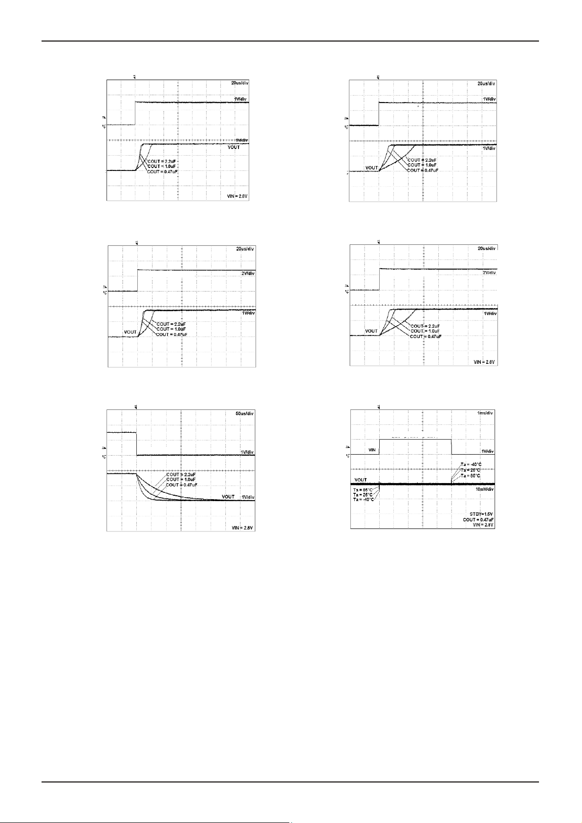
VIN=2.8V
STBY=1.5V
COUT=0.47uF
Fig.67. Load Response
IOUT=100mA→0mA
1.90
V
e
1.85
1.80
ut Volta
Out
1.75
VIN=2.8V
STBY=1.5V
COUT=0.47uF
Fig.69. Load Response
IOUT=200mA→0mA
2.00
V
e
1.90
1.80
ut Volta
Out
1.70
VIN=2.8V
STBY=1.5V
COUT=0.47uF
Fig.71. Load Response
IOUT=100mA→50mA
1.85
V
e
1.80
1.75
ut Volta
Out
1.70
Fig.73. Load Response
VIN=2.8V
STBY=1.5V
COUT=0.47uF
Output Current (mA)
100
50
0
Output Current (mA)
100
50
0
Output Current (mA)
200
100
0
Output Current (mA)
100
50
0
www.rohm.com
© 2011 ROHM Co., Ltd. All rights reserved.
12/41
2011.07 - Rev.C
Page 13
BU□□TD2WNVX series
●Reference data BU18TD2WNVX (Ta=25℃ unless otherwise specified.)
STBY=0→1.5V
2.0
1.0
0.0
Output Voltage (V)
STBY Voltage (V)
2.0
1.0
0.0
Fig.74. Start Up Time
Iout=0mA
VIN=STBY=0→2.8V
STBY Voltage (V)
4.0
2.0
0.0
2.0
1.0
0.0
Output Voltage (V)
2.0
1.0
0.0
Output Voltage (V)
Fig.76. Start Up Time
(VIN=STBY) Iout=0mA
Iout=0mA
STBY=1.5→0V
STBY Voltage (V)
2.0
1.0
0.0
Fig.78. Discharge Time
Technical Note
STBY=0→1.5V
2.0
1.0
0.0
Output Voltage (V)
Fig.75. Start Up Time
Iout=200mA
VIN=STBY=2.8→0V
2.0
1.0
0.0
Output Voltage (V)
Fig.77. Start Up Time
(VIN=STBY) Iout=200mA
VIN=2.8V→3.8V→2.8V
1.81
1.80
1.79
Output Voltage (V)
1.78
Fig.79. VIN Response
STBY Voltage (V)
2.0
1.0
0.0
STBY Voltage (V)
4.0
2.0
0.0
Input Voltage (V)
4.8
3.8
2.8
www.rohm.com
© 2011 ROHM Co., Ltd. All rights reserved.
13/41
2011.07 - Rev.C
Page 14

BU□□TD2WNVX series
)
●Reference data BU19TD2WNVX (Ta=25℃ unless otherwise specified.)
2.0
Temp=25°C
1.8
1.6
1.4
1.2
1.0
0.8
0.6
Output Voltage (V)
0.4
0.2
0.0
0 0.5 1 1.5 2 2.5 3 3 .5 4 4.5 5 5.5
Io=0uA
Io=100uA
Io=50mA
Io=200mA
Input Voltage (V)
Fig.80. Output Voltage Fig.81. Line Regulation
1.95
Temp=25°C
1.94
1.93
1.92
1.91
1.90
1.89
1.88
Output Voltage (V)
1.87
1.86
1.85
1.81.9 2 2.12.22.32.42.5
Io=0uA
Io=1 00uA
Io=50mA
Io=200mA
Input Voltage (V)
1.6
1.4
1.2
1.0
0.8
0.6
0.4
STBY Pin Curr ent ( uA)
0.2
0.0
00.511.522.5 33.544.555.5
Temp=25°C
Temp=85°C
Temp= -40°C
Input Voltage (V)
100
VIN= 3.9V
STBY=1.5V
80
60
40
Gnd Current (uA)
20
0
0 0.05 0.1 0.15 0.2
Temp=85°C
Temp=-40°C
Temp=25°C
Output Current (A)
Fig.83. VSTBY - ISTBY
Fig.84. IOUT - IGND
2.0
1.8
1.6
1.4
1.2
1.0
0.8
0.6
Output Voltage (V
0.4
0.2
0.0
VIN=5.5V
0 0.1 0.2 0.3 0.4 0.5 0.6
VIN=2.9V
VIN=2 .4V
Tem p=2 5°C
STBY=1.5V
Output Current (A)
Fig.86. OCP Threshold
2.0
VIN= 3.9V
Io=0mA
1.5
1.0
0.5
Output Voltage (V)
0.0
Temp=25°C
Temp=85°C
0 0.5 1 1.5
STBY Voltage (V )
Fig.87. STBY Threshold Fig.88. VOUT - Temp
60
VIN= 2.9V
STBY=1.5V
50
Io=0µA
40
30
20
Gnd Current (uA)
10
0
-40 -15 10 35 60 85
Temp ( °C)
1.0
0.9
0.8
0.7
0.6
0.5
0.4
0.3
Gnd Current (uA)
0.2
0.1
0.0
-40 -15 10 35 60 85
Temp ( °C)
Fig.89. IGND - Temp
Fig.90. IGND - Temp (STBY)
VIN= STBY
Temp=-40°C
VIN= 2.9V
STBY=0V
Technical Note
100
IO=0uA
80
60
40
Gnd Current (uA)
20
0
0 0.5 1 1.5 2 2.5 3 3.5 4 4.5 5 5.5
Input Voltage (V)
Fig.82. Circuit Current IGND
1.95
1.94
1.93
1.92
1.91
1.90
1.89
1.88
Output Voltage (V)
1.87
1.86
1.85
0 0.05 0.1 0.15 0.2
Temp=25°C
Temp=-40°C
Output Current (A)
Fig.85. Load Regulation
1.95
1.94
1.93
1.92
1.91
1.90
1.89
1.88
Output Voltage (V)
1.87
1.86
1.85
-40 - 15 10 35 60 85
Temp ( °C)
VIN= STBY
Temp=85°C
Temp=25°C
Temp= -40°C
VIN= 2.9V
STBY=1.5V
Temp=85°C
VIN= 2.9V
STBY=1.5V
Io=100µA
www.rohm.com
© 2011 ROHM Co., Ltd. All rights reserved.
14/41
2011.07 - Rev.C
Page 15

BU□□TD2WNVX series
p
g
(
)
p
g
(
)
p
g
(
)
p
g
(
)
p
g
(
)
p
g
(
)
p
g
(
)
p
g
(
)
●Reference data BU19TD2WNVX (Ta=25℃ unless otherwise specified.)
IOUT=0mA→50mA
V
e
ut Volta
Out
1.95
1.90
1.85
1.80
Output Current (mA)
100
50
0
Fig.91. Load Response
IOUT=0mA→100mA
V
e
ut Volta
Out
1.95
1.90
1.85
1.80
Output Current (mA)
100
50
0
Fig.93. Load Response
IOUT=0mA→200mA
V
e
ut Volta
Out
2.00
1.90
1.80
1.70
Output Current (mA)
200
100
0
Fig.95. Load Response
IOUT=50mA→100mA
V
e
ut Volta
Out
1.95
1.90
1.85
1.80
Output Current (mA)
100
50
0
Fig.97. Load Response
V
e
ut Volta
Out
V
e
ut Volta
Out
V
e
ut Volta
Out
V
e
ut Volta
Out
2.00
1.95
1.90
1.85
2.00
1.95
1.90
1.85
2.10
2.00
1.90
1.80
2.00
1.95
1.90
1.85
Technical Note
IOUT=50mA→0mA
Fig.92. Load Response
IOUT=100mA→0mA
Fig.94. Load Response
IOUT=200mA→0mA
Fig.96. Load Response
IOUT=100mA→50mA
Fig.98. Load Response
Output Current (mA)
100
50
0
Output Current (mA)
100
50
0
Output Current (mA)
200
100
0
Output Current (mA)
100
50
0
www.rohm.com
© 2011 ROHM Co., Ltd. All rights reserved.
15/41
2011.07 - Rev.C
Page 16

BU□□TD2WNVX series
p
g
(
)
●Reference data BU19TD2WNVX (Ta=25℃ unless otherwise specified.)
STBY=0→1.5V
2.0
1.0
0.0
Output Voltage (V)
STBY Voltage (V)
2.0
1.0
0.0
Fig.99. Start Up Time
Iout=0mA
VIN=STBY=0→2.9V
2.0
1.0
0.0
Output Voltage (V)
STBY Voltage (V)
4.0
2.0
0.0
Fig.101. Start Up Time
(VIN=STBY) Iout=0mA
STBY=1.5→0V
2.0
1.0
0.0
Output Voltage (V)
STBY Voltage (V)
2.0
1.0
0.0
Fig.103. Discharge Time
Technical Note
STBY=0→1.5V
2.0
1.0
0.0
Output Voltage (V)
Fig.100. Start Up Time
Iout=200mA
VIN=STBY=0→2.9V
2.0
1.0
0.0
Output Voltage (V)
Fig.102. Start Up Time
(VIN=STBY) Iout=200mA
VIN=2.9V→3.9V→2.9V
1.91
V
e
1.90
1.89
ut Volta
Out
1.88
Fig.104. VIN Response
STBY Voltage (V)
2.0
1.0
0.0
STBY Voltage (V)
4.0
2.0
0.0
Input Voltage (V)
4.9
3.9
2.9
www.rohm.com
© 2011 ROHM Co., Ltd. All rights reserved.
16/41
2011.07 - Rev.C
Page 17

BU□□TD2WNVX series
●Reference data BU25TD2WNVX (Ta=25℃ unless otherwise specified.)
3.5
Temp=25°C
3.0
2.5
2.0
1.5
1.0
Output Voltage (V)
0.5
0.0
00.511.522.533.544.555.5
Io=0uA
Io=100uA
Io=50mA
Io=200mA
Input Voltage (V)
VIN= STBY
2.55
Temp=25°C
2.54
2.53
2.52
2.51
2.50
2.49
2.48
Output Voltage (V)
2.47
2.46
2.45
2.4 2.5 2.6 2.7 2.8 2.9 3 3.1
Io=0uA
Io=100uA
Io=50mA
Io=200mA
Input Voltage (V)
Fig.105. Output Voltage Fig.106. Line Regulation
1.6
1.4
1.2
1.0
0.8
0.6
0.4
STBY Pin Curr ent ( uA)
0.2
0.0
00.511.522.5 33.544.555.5
Temp=85°C
Temp=25°C
Input Voltage (V)
Temp=- 40°C
100
VIN= 3.5V
STBY=1.5V
80
60
40
Gnd Current (uA)
20
0
0 0.05 0.1 0.15 0.2
Temp=85°C
Temp=-40°C
Temp=25°C
Output Current (A)
Fig.108. VSTBY - ISTBY
Fig.109. IOUT - IGND
0.35
0.30
0.25
0.20
0.15
Dropout Voltage ( V)
Temp= -40°C
0.10
0.05
0.00
0 0.05 0.1 0.15 0.2
Temp=85°C
Temp=25°C
VIN = 0.98 x VOUT
STBY=1.5V
Output Current (A)
3.0
Temp =25° C
2.5
2.0
1.5
1.0
Output Voltage (V)
0.5
0.0
VIN=5.5V
0 0.1 0.2 0.3 0.4 0.5 0.6
VIN=3 .5V
Output Current (A)
VIN=3.0V
Fig.111. Dropout Voltage
Fig.112. OCP Threshold
2.55
2.54
2.53
2.52
2.51
2.50
2.49
2.48
Output Voltage ( V)
2.47
2.46
2.45
-40 -15 10 35 60 85
Temp ( °C)
VIN= 3.5V
STBY=1.5V
Io=0.1mA
60
VIN= 3.5V
STBY=1.5V
50
Io=0mA
40
30
20
Gnd Current (uA)
10
0
-40 -15 10 35 60 85
Temp ( °C)
Fig.114. VOUT - Temp
Fig.115. IGND - Temp
VIN= STBY
STBY=1.5V
Technical Note
100
IO=0uA
80
60
40
Gnd Current (uA)
20
0
00.511.522.533.544.555.5
Input Voltage (V)
Fig.107. Circuit Current IGND
2.55
2.54
2.53
2.52
2.51
2.50
2.49
2.48
Output Voltage (V)
2.47
2.46
2.45
0 0.05 0.1 0.15 0.2
Temp=25°C
Temp=-40°C
Output Current (A)
Fig.110. Load Regulation
3.0
VIN= 3.5V
2.5
Io=0mA
2.0
1.5
1.0
Output Voltage (V)
0.5
0.0
Temp=25°C
Temp=85°C
0 0.5 1 1.5
STBY Voltage (V )
Fig.113. STBY Threshold
1.0
0.9
0.8
0.7
0.6
0.5
0.4
0.3
Gnd Current (uA)
0.2
0.1
0.0
-40 -15 10 35 60 85
Temp ( °C)
Fig.116. IGND - Temp (STBY)
Temp=85°C
Temp=25°C
Temp=85°C
Temp=-40°C
VIN= STBY
Temp= -40°C
VIN= 3.5V
STBY=1.5V
VIN= 3.5V
STBY=0V
www.rohm.com
© 2011 ROHM Co., Ltd. All rights reserved.
17/41
2011.07 - Rev.C
Page 18

BU□□TD2WNVX series
p
g
(
)
p
g
(
)
p
g
(
)
p
g
(
)
p
g
(
)
p
g
(
)
p
g
(
)
p
g
(
)
●Reference data BU25TD2WNVX (Ta=25℃ unless otherwise specified.)
IOUT=0mA→50mA
V
e
ut Volta
Out
2.55
2.50
2.45
2.40
Output Current (mA)
100
50
0
Fig.117. Load Response
IOUT=0mA→100mA
V
e
ut Volta
Out
2.55
2.50
2.45
2.40
Output Current (mA)
100
50
0
Fig.119. Load Response
IOUT=0mA→200mA
V
e
ut Volta
Out
2.60
2.50
2.40
2.30
Output Current (mA)
200
100
0
Fig.121. Load Response
IOUT=50mA→100mA
V
e
ut Volta
Out
2.55
2.50
2.45
2.40
Output Current (mA)
100
50
0
Fig.123. Load Response
V
e
ut Volta
Out
V
e
ut Volta
Out
V
e
ut Volta
Out
V
e
ut Volta
Out
2.70
2.65
2.50
2.45
2.60
2.55
2.50
2.45
2.70
2.60
2.50
2.40
2.0
2.55
2.50
2.45
Technical Note
IOUT=50mA→0mA
Fig.118. Load Response
IOUT=100mA→0mA
Fig.120. Load Response
IOUT=200mA→0mA
Fig.122. Load Response
IOUT=100mA→50mA
Fig.124. Load Response
Output Current (mA)
100
50
0
Output Current (mA)
200
100
0
Output Current (mA)
200
100
0
Output Current (mA)
100
50
0
www.rohm.com
© 2011 ROHM Co., Ltd. All rights reserved.
18/41
2011.07 - Rev.C
Page 19

BU□□TD2WNVX series
p
g
(
)
●Reference data BU25TD2WNVX (Ta=25℃ unless otherwise specified.)
STBY=0→1.5V
4.0
2.0
0.0
Output Voltage (V)
STBY Voltage (V)
2.0
1.0
0.0
Fig.125. Start Up Time
Iout=0mA
VIN=STBY=0→3.5V
4.0
2.0
0.0
Output Voltage (V)
STBY Voltage (V)
4.0
2.0
0.0
Fig.127. Start Up Time
(VIN=STBY) Iout=0mA
STBY=1.5→0V
4.0
2.0
0.0
Output Voltage (V)
STBY Voltage (V)
2.0
1.0
0
Fig.129. Discharge Time
Technical Note
STBY=0→1.5V
4.0
2.0
0.0
Output Voltage (V)
Fig.126. Start Up Time
Iout=200mA
VIN=STBY=0→3.5V
4.0
2.0
0.0
Output Voltage (V)
Fig.128. Start Up Time
(VIN=STBY) Iout=200mA
VIN=3.5V→4.5V→3.5V
2.51
V
e
2.50
2.49
ut Volta
Out
2.48
Fig.130. VIN Response
STBY Voltage (V)
2.0
1.0
0.0
STBY Voltage (V)
4.0
2.0
0.0
Input Voltage (V)
5.5
4.5
3.5
www.rohm.com
© 2011 ROHM Co., Ltd. All rights reserved.
19/41
2011.07 - Rev.C
Page 20

BU□□TD2WNVX series
●Reference data BU26TD2WNVX (Ta=25℃ unless otherwise specified.)
3.0
Temp=25°C
2.5
2.0
1.5
1.0
Output Voltage (V)
0.5
0.0
00.511.522.533.544.555.5
Io=0uA
Io=1 00uA
Io=50mA
Io=200mA
Input Voltage (V)
VIN= STBY
2.65
Temp=25°C
2.64
2.63
2.62
2.61
2.60
2.59
2.58
Output Voltage (V)
2.57
2.56
2.55
2.5 2.6 2.7 2.8 2.9 3 3.1 3.2
Io=0uA
Io=100uA
Io=50mA
Io=200mA
Input Voltage (V)
Fig.131. Output Voltage
Fig.132. Line Regulation
1.6
1.4
1.2
1.0
0.8
0.6
0.4
STBY Pin Curr ent ( uA)
0.2
0.0
00.511.522.5 33.544.555.5
Temp=85°C
Temp=25°C
Input Voltage (V)
Temp=- 40°C
100
VIN= 3.6V
STBY=1.5V
80
60
40
Gnd Current (uA)
20
0
0 0.05 0.1 0.15 0.2
Temp=85°C
Temp=-40°C
Temp=25°C
Output Current (A)
Fig.134. VSTBY - ISTBY
Fig.135. IOUT - IGND Fig.136. Load Regulation
0.35
0.30
0.25
0.20
0.15
Dropout Voltage ( V)
Temp=-40°C
0.10
0.05
0.00
0 0.05 0.1 0.15 0.2
Temp=85°C
Temp=25°C
VIN = 0.98 x VOUT
STBY=1.5V
Output Current (A)
3.0
Temp=25°C
2.5
2.0
1.5
1.0
Output Voltage (V)
0.5
0.0
VIN=5.5V
0 0.1 0.2 0.3 0.4 0.5 0.6
Output Current (A)
VIN=3.6V
Fig.137. Dropout Voltage
Fig.138. OCP Threshold
2.65
2.64
2.63
2.62
2.61
2.60
2.59
2.58
Output Voltage (V)
2.57
2.56
2.55
-40 -15 10 35 60 85
Temp ( °C)
VIN= 3.6V
STBY=1.5V
Io=0.1mA
60
VIN= 3.6V
STBY=1.5V
50
Io=0mA
40
30
20
Gnd Current (uA)
10
0
-40 -15 10 35 60 85
Temp ( °C)
Fig.140. VOUT - Temp
Fig.141. IGND - Temp Fig.142. IGND - Temp (STBY)
VIN= STBY
VIN=3.1V
STBY=1.5V
Technical Note
100
IO=0uA
80
60
40
Gn d Cu rren t (u A)
20
0
00.511.522.533.544.555.5
Fig.133. Circuit Current IGND
2.65
2.64
2.63
2.62
2.61
2.60
2.59
2.58
Output Voltage (V)
2.57
2.56
2.55
0 0.05 0.1 0.15 0.2
3.0
2.5
2.0
1.5
1.0
Output Voltage (V)
0.5
0.0
0 0.5 1 1.5
Fig.139. STBY Threshold
1.0
0.9
0.8
0.7
0.6
0.5
0.4
0.3
Gnd Current (uA)
0.2
0.1
0.0
-40 -15 10 35 60 85
VIN= 3.6V
STBY=1.5V
Temp=-40°C
VIN= 3.6V
Io=0mA
Temp=25°C
Temp=85°C
Input Voltage (V)
Temp=25°C
Temp=85°C
Output Current (A)
STBY Voltage (V )
Temp ( °C)
VIN=ST BY
Temp=85°C
Temp= 25°C
Temp=-40°C
Temp=-40°C
VIN= 3.6V
STBY=0V
www.rohm.com
© 2011 ROHM Co., Ltd. All rights reserved.
20/41
2011.07 - Rev.C
Page 21

BU□□TD2WNVX series
p
g
(
)
p
g
(
)
p
g
(
)
p
g
(
)
p
g
(
)
p
g
(
)
p
g
(
)
p
g
(
)
●Reference data BU26TD2WNVX (Ta=25℃ unless otherwise specified.)
V
e
ut Volta
Out
2.65
2.60
2.55
2.50
IOUT=0mA→50mA
Fig.143. Load Response
Output Current (mA)
100
50
0
V
e
ut Volta
Out
IOUT=0mA→100mA
2.65
2.60
2.55
2.50
Output Current (mA)
100
50
0
Fig.145. Load Response
V
e
ut Volta
Out
2.70
2.60
2.50
2.40
IOUT=0mA→200mA
Output Current (mA)
200
100
0
Fig.147. Load Response
V
e
ut Volta
Out
2.65
2.60
2.55
2.50
IOUT=50mA→100mA
Output Current (mA)
100
50
0
Fig.149. Load Response
V
e
ut Volta
Out
V
e
ut Volta
Out
V
e
ut Volta
Out
V
e
ut Volta
Out
2.60
2.59
2.60
2.55
2.62
2.61
2.70
2.65
2.60
2.55
2.80
2.70
2.60
2.50
2.70
2.65
Technical Note
IOUT=50mA→0mA
Fig.144. Load Response
IOUT=100mA→0mA
Fig.146. Load Response
IOUT=200mA→0mA
Fig.148. Load Response
IOUT=100mA→50mA
Fig.150. Load Response
Output Current (mA)
100
50
0
Output Current (mA)
100
50
0
Output Current (mA)
200
100
0
Output Current (mA)
100
50
0
www.rohm.com
© 2011 ROHM Co., Ltd. All rights reserved.
21/41
2011.07 - Rev.C
Page 22

BU□□TD2WNVX series
p
g
(
)
●Reference data BU26TD2WNVX (Ta=25℃ unless otherwise specified.)
STBY=0→1.5V
4.0
2.0
0.0
Output Voltage (V)
STBY Voltage (V)
2.0
1.0
0.0
Fig.151. Start Up Time
Iout=0mA
VIN=STBY=0→3.6V
4.0
2.0
0.0
Output Voltage (V)
STBY Voltage (V)
4.0
2.0
0.0
Fig.153. Start Up Time
(VIN=STBY) Iout=0mA
STBY=1.5→0V
4.0
2.0
0.0
Output Voltage (V)
STBY Voltage (V)
2.0
1.0
0.0
Fig.155. Discharge Time
V
e
ut Volta
Out
Technical Note
STBY=0→1.5V
4.0
2.0
0.0
Output Voltage (V)
Fig.152. Start Up Time
Iout=200mA
VIN=STBY=0→3.6V
4.0
2.0
0.0
Output Voltage (V)
Fig.154. Start Up Time
(VIN=STBY) Iout=200mA
VIN=3.6V→4.6V→3.6V
2.65
2.60
2.55
Fig.156. VIN Response
STBY Voltage (V)
2.0
1.0
0.0
STBY Voltage (V)
4.0
2.0
0.0
Input Voltage (V)
5.6
4.6
3.6
www.rohm.com
© 2011 ROHM Co., Ltd. All rights reserved.
22/41
2011.07 - Rev.C
Page 23

BU□□TD2WNVX series
●Reference data BU27TD2WNVX (Ta=25℃ unless otherwise specified.)
3.0
Temp=25°C
2.5
2.0
1.5
1.0
Output Voltage (V)
0.5
0.0
00.511.522.533.544.555.5
Io=0uA
Io=1 00uA
Io=50mA
Io=200mA
Input Voltage (V)
VIN= STBY
2.75
Temp=25°C
2.74
2.73
2.72
2.71
2.70
2.69
2.68
Output Voltage (V)
2.67
2.66
2.65
2.62.72.82.9 3 3.13.23.3
Io=0uA
Io=100uA
Io=50mA
Io=200mA
Input Voltage (V)
Fig.157. Output Voltage Fig.158. Line Regulation
1.6
1.4
1.2
1.0
0.8
0.6
0.4
STBY Pin Curr ent ( uA)
0.2
0.0
00.511.522.5 33.544.555.5
Temp=85°C
Temp=25°C
Input Voltage (V)
Temp=- 40°C
100
VIN= 3.7V
STBY=1.5V
80
60
40
Gnd Current (uA)
20
0
0 0.05 0.1 0.15 0.2
Temp=85°C
Temp=-40°C
Temp=25°C
Output Current (A)
Fig.160. VSTBY - ISTBY
Fig.161. IOUT - IGND
0.35
0.30
0.25
0.20
Temp=-40°C
0.15
0.10
Dropout Voltage (V)
0.05
0.00
0 0.05 0 .1 0.15 0.2
Fig.163. Dropout Voltage
Temp=85°C
Temp=25°C
VIN = 0.98 x VOUT
Output Current (A)
STBY=1.5V
3.0
2.5
2.0
1.5
1.0
Output Voltage (V)
0.5
0.0
0 0.1 0.2 0.3 0.4 0.5 0.6
VIN=5.5V
VIN=3 .6V
Output Current (A)
Fig.164. OCP Threshold
2.75
2.74
2.73
2.72
2.71
2.70
2.69
2.68
Output Voltage (V)
2.67
2.66
2.65
-40 -15 10 35 60 85
Temp ( °C)
VIN= 3.7V
STBY=1.5V
Io=0.1mA
60
VIN= 3.7V
STBY=1.5V
50
Io=0.1mA
40
30
20
Gnd Current (uA)
10
0
-40 -15 10 35 60 85
Temp ( °C)
Fig.166. VOUT - Temp Fig.167. IGND - Temp
VIN= STBY
VIN=3. 1V
Temp =25° C
STBY=1.5V
Technical Note
100
IO=0uA
80
60
40
Gn d Cu rren t (u A)
20
0
00.511.522.533.544.555.5
Fig.159. Circuit Current IGND
2.75
2.74
2.73
2.72
2.71
2.70
2.69
2.68
Output Voltage (V)
2.67
2.66
2.65
0 0.05 0 .1 0.15 0.2
Fig.162. Load Regulation
3.0
2.5
2.0
1.5
1.0
Output Voltage (V)
0.5
0.0
0 0.5 1 1.5
Fig.165. STBY Threshold
1.0
0.9
0.8
0.7
0.6
0.5
0.4
0.3
Gnd Current (uA)
0.2
0.1
0.0
-40 -15 10 35 60 85
Fig.168. IGND - Temp (STBY)
VIN= 3.7V
STBY=1.5V
Temp=-40°C
VIN= 3.7V
Io=0mA
Input Voltage (V)
Temp=25°C
Output Current (A)
Temp=25°C
Temp=85°C
STBY Voltage (V )
Temp ( °C)
VIN=ST BY
Temp= 85°C
Temp= 25°C
Temp= -40°C
Temp=85°C
Temp=-40°C
VIN= 3.7V
STBY=0V
www.rohm.com
© 2011 ROHM Co., Ltd. All rights reserved.
23/41
2011.07 - Rev.C
Page 24

BU□□TD2WNVX series
p
g
(
)
p
g
(
)
p
g
(
)
p
g
(
)
p
g
(
)
p
g
(
)
p
g
(
)
p
g
(
)
●Reference data BU27TD2WNVX (Ta=25℃ unless otherwise specified.)
IOUT=0mA→50mA
V
e
ut Volta
Out
2.75
2.70
2.65
2.60
Output Current (mA)
100
50
0
Fig.169. Load Response
IOUT=0mA→100mA
V
e
ut Volta
Out
2.75
2.70
2.65
2.60
Output Current (mA)
100
50
0
Fig.171. Load Response
IOUT=0mA→200mA
V
e
ut Volta
Out
2.80
2.70
2.60
2.50
Output Current (mA)
200
100
0
Fig.173. Load Response
IOUT=50mA→100mA
V
e
ut Volta
Out
2.75
2.70
2.65
2.60
Output Current (mA)
100
50
0
Fig.175. Load Response
Technical Note
IOUT=50mA→0mA
2.80
V
e
2.75
2.70
ut Volta
Out
2.65
Fig.170. Load Response
IOUT=100mA→0mA
2.80
V
e
2.75
2.70
ut Volta
Out
2.65
Fig.172. Load Response
IOUT=200mA→0mA
2.90
V
e
2.80
2.70
ut Volta
Out
2.60
Fig.174. Load Response
IOUT=100mA→50mA
2.80
V
e
2.75
2.70
ut Volta
Out
2.65
Fig.176. Load Response
Output Current (mA)
100
50
0
Output Current (mA)
100
50
0
Output Current (mA)
200
100
0
Output Current (mA)
100
50
0
www.rohm.com
© 2011 ROHM Co., Ltd. All rights reserved.
24/41
2011.07 - Rev.C
Page 25

BU□□TD2WNVX series
p
g
(
)
●Reference data BU27TD2WNVX (Ta=25℃ unless otherwise specified.)
STBY=0→1.5V
4.0
2.0
0.0
Output Voltage (V)
STBY Voltage (V)
2.0
1.0
0.0
Fig.177. Start Up Time
Iout=0mA
VIN=STBY=0→3.7V
4.0
2.0
0.0
Output Voltage (V)
STBY Voltage (V)
4.0
2.0
0.0
Fig.179. Start Up Time
(VIN=STBY) Iout=0mA
STBY=1.5→0V
4.0
2.0
0.0
Output Voltage (V)
STBY Voltage (V)
2.0
1.0
0.0
Fig.181. Discharge Time
Technical Note
STBY=0→1.5V
4.0
2.0
0.0
Output Voltage (V)
Fig.178. Start Up Time
Iout=200mA
VIN=STBY=0→3.7V
4.0
2.0
0.0
Output Voltage (V)
Fig.180. Start Up Time
(VIN=STBY) Iout=200mA
2.71
V
e
2.70
2.69
ut Volta
Out
2.68
Fig.182. VIN Response
STBY Voltage (V)
2.0
1.0
0.0
STBY Voltage (V)
4.0
2.0
0.0
Input Voltage (V)
5.7
4.7
3.7
www.rohm.com
© 2011 ROHM Co., Ltd. All rights reserved.
25/41
2011.07 - Rev.C
Page 26

BU□□TD2WNVX series
)
●Reference data BU28TD2WNVX (Ta=25℃ unless otherwise specified.)
3.0
Temp=25°C
2.5
2.0
1.5
1.0
Output Voltage (V)
0.5
0.0
00.511.522.533.544.555.5
Io=0uA
Io=1 00uA
Io=50mA
Io=200mA
Input Voltage (V)
VIN= STBY
2.85
Temp=25°C VIN=ST BY
2.84
2.83
2.82
2.81
2.80
2.79
2.78
Output Voltage (V)
2.77
2.76
2.75
2.7 2.8 2.9 3 3.1 3.2 3.3 3.4
Io=0uA
Io=1 00uA
Io=50mA
Io=200mA
Input Voltage (V)
Fig.183. Output Voltage Fig.184. Line Regulation Fig.185. Circuit Current IGND
1.6
1.4
1.2
1.0
0.8
0.6
0.4
STBY Pin Curr ent ( uA)
0.2
0.0
00.511.522.5 33.544.555.5
Temp=85°C
Temp=25°C
Input Voltage (V)
Temp=- 40°C
100
VIN= 3.8V
STBY= 1.5V
80
60
40
Gnd Curr ent (uA)
20
0
0 0.05 0.1 0.15 0.2
Temp=85°C
Temp=-40°C
Temp=25°C
Output Current (A )
Fig.186. VSTBY - ISTBY
Fig.187. IOUT - IGND
0.35
0.30
0.25
0.20
0.15
Temp=-40°C
0.10
Dropout Voltage (V)
0.05
0.00
0 0.05 0 .1 0.15 0.2
Temp=85°C
Temp=25°C
VIN = 0.98 x VOUT
Output Current (A)
STBY=1.5V
3.0
2.5
2.0
1.5
1.0
Output Voltage (V
0.5
0.0
VIN=5.5V
0 0.1 0.2 0.3 0.4 0.5 0.6
Output Current (A)
VIN=3.8V
Fig.189. Dropout Voltage
Fig.190. OCP Threshold
2.85
2.84
2.83
2.82
2.81
2.80
2.79
2.78
Output Voltage (V)
2.77
2.76
2.75
-40 -15 10 35 60 85
Temp ( °C)
VIN= 3.8V
STBY= 1.5V
Io=0.1mA
60
VIN= 3.8V
STBY= 1.5V
50
Io=0mA
40
30
20
Gnd Current (uA)
10
0
-40 -15 10 35 60 85
Temp ( °C)
Fig.192. VOUT - Temp
Fig.193. IGND - Temp Fig.194. IGND - Temp (STBY)
VIN=3 .3V
Tem p=2 5°C
STBY=1.5V
Technical Note
100
Io=0uA
80
60
40
Gnd Cur rent (uA)
20
0
00.511.522.533.544.555.5
Input Voltage (V )
2.85
VIN= 3.8V
2.84
STBY=1.5V
2.83
2.82
2.81
2.80
2.79
2.78
Output Voltage (V)
2.77
2.76
Temp=-40°C
2.75
0 0.05 0 .1 0.15 0.2
Temp=25°C
Temp=85°C
Output Current (A)
Fig.188. Load Regulation
3.0
VIN= 3.8V
2.5
Io=0mA
2.0
1.5
1.0
Output Voltage (V)
0.5
0.0
Temp=25°C
Temp=85°C
00.511.5
STBY V oltage (V)
Fig.191. STBY Threshold
1.0
0.9
0.8
0.7
0.6
0.5
0.4
0.3
Gnd Current (uA)
0.2
0.1
0.0
-40 -15 10 35 60 85
Temp ( °C)
VIN=ST BY
Temp=85°C
Temp=25°C
Temp=-40°C
Temp=-40°C
VIN= 3.8V
STBY= 0V
www.rohm.com
© 2011 ROHM Co., Ltd. All rights reserved.
26/41
2011.07 - Rev.C
Page 27

BU□□TD2WNVX series
p
g
(
)
p
g
(
)
p
g
(
)
p
g
(
)
p
g
(
)
p
g
(
)
p
g
(
)
p
g
(
)
●Reference data BU28TD2WNVX (Ta=25℃ unless otherwise specified.)
IOUT=0mA→50mA
V
e
ut Volta
Out
2.85
2.80
2.75
2.70
Output Current (mA)
100
50
0
Fig.195. Load Response
IOUT=0mA→100mA
V
e
ut Volta
Out
2.85
2.80
2.75
2.70
Output Current (mA)
100
50
0
Fig.197. Load Response
IOUT=0mA→200mA
V
e
ut Volta
Out
2.90
2.80
2.70
2.60
Output Current (mA)
200
100
0
Fig.199. Load Response
IOUT=50mA→100mA
V
e
ut Volta
Out
2.85
2.80
2.75
2.70
Output Current (mA)
100
50
0
Fig.201. Load Response
V
e
ut Volta
Out
2.80
2.75
2.90
2.85
V
e
ut Volta
Out
V
e
ut Volta
Out
V
e
ut Volta
Out
2.80
2.75
2.80
2.75
2.80
2.70
2.90
2.85
2.90
2.85
3.00
2.90
Technical Note
Fig.196. Load Response
IOUT=100mA→0mA
Fig.198. Load Response
IOUT=200mA→0mA
Fig.200. Load Response
IOUT=100mA→50mA
Fig.202. Load Response
Output Current (mA)
100
50
0
Output Current (mA)
100
50
0
Output Current (mA)
200
100
0
Output Current (mA)
100
50
0
www.rohm.com
© 2011 ROHM Co., Ltd. All rights reserved.
27/41
2011.07 - Rev.C
Page 28

BU□□TD2WNVX series
p
g
(
)
●Reference data BU28TD2WNVX (Ta=25℃ unless otherwise specified.)
STBY=0→1.5V
4.0
2.0
0.0
Output Voltage (V)
STBY Voltage (V)
2.0
1.0
0.0
Fig.203. Start Up Time
Iout=0mA
VIN=STBY=0→3.8V
4.0
2.0
0.0
Output Voltage (V)
STBY Voltage (V)
4.0
2.0
0.0
Fig.205. Start Up Time
(VIN=STBY) Iout=0mA
4.0
2.0
0.0
Output Voltage (V)
STBY=1.5→0V
STBY Voltage (V)
2.0
1.0
0.0
Fig.207. Discharge Time
V
e
ut Volta
Out
Technical Note
STBY Voltage (V)
2.0
STBY=0→1.5V
4.0
2.0
0.0
Output Voltage (V)
Fig.204. Start Up Time
Iout=200mA
VIN=STBY=0→3.8V
4.0
2.0
0.0
Output Voltage (V)
Fig.206. Start Up Time
(VIN=STBY) Iout=200mA
VIN=3.8→4.8V→3.8V
2.81
2.80
2.79
2.78
Fig.208. VIN Response
1.0
0.0
STBY Voltage (V)
4.0
2.0
0.0
Input Voltage (V)
5.8
4.8
3.8
www.rohm.com
© 2011 ROHM Co., Ltd. All rights reserved.
28/41
2011.07 - Rev.C
Page 29

BU□□TD2WNVX series
●Reference data BU30TD2WNVX (Ta=25℃ unless otherwise specified.)
3.5
Temp=25°C
3.0
2.5
2.0
1.5
1.0
Output Voltage (V)
0.5
0.0
00.511.522.533.544.555.5
Io=0uA
Io=1 00uA
Io=50mA
Io=200mA
Input Voltage (V)
VIN= STBY
3.05
Temp=25°C
3.04
3.03
3.02
3.01
3.00
2.99
2.98
Output Voltage (V)
2.97
2.96
2.95
2.9 3 3.13.2 3.33.4 3.53.6
Io=0uA
Io=1 00uA
Io=50mA
Io=2 00mA
Input Voltage (V)
Fig.209. Output Voltage Fig.210. Line Regulation
1.6
1.4
1.2
1.0
0.8
0.6
0.4
STBY Pin Curr ent ( uA)
0.2
0.0
00.511.522.5 33.544.555.5
Temp=85°C
Temp=25°C
Input Voltage (V)
Temp=-40°C
100
VIN= 4.0V
STBY= 1.5V
80
60
40
Gnd Current (uA)
20
0
0 0.05 0.1 0.15 0.2
Temp=85°C
Temp=-40°C
Temp=25°C
Output Cur rent (A )
Fig.212. VSTBY - ISTBY
Fig.213. IOUT - IGND
0.30
0.25
0.20
0.15
0.10
Dropout Voltage ( V)
0.05
0.00
Temp= -40°C
0 0.05 0.1 0.15 0.2
Temp=85°C
Temp=25°C
VIN = 0.98 x VOUT
STBY=1.5V
Output Current (A)
3.5
3.0
2.5
2.0
1.5
1.0
Output Voltage (V)
0.5
0.0
0 0.10.20.30.40.50.6
VIN=5.5V
VIN=3.5V
Output Current (A )
Fig.215. Dropout Voltage
Fig.216. OCP Threshold
3.05
3.04
3.03
3.02
3.01
3.00
2.99
2.98
Output Voltage (V)
2.97
2.96
2.95
-40 -15 10 35 60 85
Temp ( °C)
VIN= 4.0V
STBY=1.5V
Io=0.1mA
60
VIN= 4.0V
STBY=1.5V
50
Io=0mA
40
30
20
Gnd Curr ent (uA)
10
0
-40 -15 10 35 60 85
Temp ( °C)
Fig.218. VOUT - Temp
Fig.219. IGND - Temp Fig.220. IGND - Temp (STBY)
VIN=ST BY
VIN=4.0V
Temp=25°C
STBY= 1.5V
Technical Note
100
Io=0uA VIN= STBY
80
60
40
Gnd Curr ent (uA)
20
0
00.511.522.533.544.555.5
Input Voltage (V)
Fig.211. Circuit Current IGND
3.05
VIN= 4.0V
3.04
STBY=1.5V
3.03
3.02
3.01
3.00
2.99
2.98
Output Voltage (V)
2.97
Temp=-40°C
2.96
2.95
0 0.05 0.1 0.15 0.2
Temp=25°C
Output Current (A)
Fig.214. Load Regulation
3.5
VIN= 4.0V
3.0
Io=0mA
2.5
2.0
1.5
1.0
Output Voltage (V)
0.5
0.0
Temp=25°C
Temp=85°C
00.511.5
STBY V oltage (V)
Fig.217. STBY Threshold
1.0
0.9
0.8
0.7
0.6
0.5
0.4
0.3
Gnd Current (uA)
0.2
0.1
0.0
-40 -15 10 35 60 85
Temp ( °C)
Temp=85°C
Temp=85°C
Temp=25°C
Temp=-40°C
Temp=-40°C
VIN= 4.0V
STBY=0V
www.rohm.com
© 2011 ROHM Co., Ltd. All rights reserved.
29/41
2011.07 - Rev.C
Page 30

BU□□TD2WNVX series
p
g
(
)
p
g
(
)
p
g
(
)
p
g
(
)
p
g
(
)
p
g
(
)
p
g
(
)
p
g
(
)
●Reference data BU30TD2WNVX (Ta=25℃ unless otherwise specified.)
IOUT=0mA→50mA
V
e
ut Volta
Out
3.05
3.00
2.95
2.90
Output Current (mA)
100
50
0
Fig.221. Load Response
IOUT=0mA→100mA
V
e
ut Volta
Out
3.05
3.00
2.95
2.90
Output Current (mA)
100
50
0
Fig.223. Load Response
IOUT=0mA→200mA
V
e
ut Volta
Out
3.10
3.00
2.90
2.80
Output Current (mA)
200
100
0
Fig.225. Load Response
IOUT=50mA→100mA
V
e
ut Volta
Out
3.05
3.00
2.95
2.90
Output Current (mA)
100
50
0
Fig.227. Load Response
Technical Note
IOUT=50mA→0mA
3.10
V
e
3.05
3.00
ut Volta
Out
2.95
Fig.222. Load Response
IOUT=100mA→0mA
3.10
V
e
3.05
3.00
ut Volta
Out
2.95
Fig.224. Load Response
IOUT=200mA→0mA
3.20
V
e
3.10
3.00
ut Volta
Out
2.90
Fig.226. Load Response
IOUT=100mA→50mA
3.10
V
e
3.05
3.00
ut Volta
Out
2.95
Fig.228. Load Response
Output Current (mA)
100
50
0
Output Current (mA)
100
50
0
Output Current (mA)
200
100
0
Output Current (mA)
100
50
0
www.rohm.com
© 2011 ROHM Co., Ltd. All rights reserved.
30/41
2011.07 - Rev.C
Page 31

BU□□TD2WNVX series
p
g
(
)
●Reference data BU30TD2WNVX (Ta=25℃ unless otherwise specified.)
STBY=0→1.5V
4.0
2.0
0.0
Output Voltage (V)
STBY Voltage (V)
2.0
1.0
0.0
Fig.229. Start Up Time
Iout=0mA
VIN=STBY=0→4.0V
4.0
2.0
0.0
Output Voltage (V)
STBY Voltage (V)
4.0
2.0
0.0
Fig.231. Start Up Time
(VIN=STBY) Iout=0mA
4.0
2.0
0.0
Output Voltage (V)
STBY=1.5→0V
STBY Voltage (V)
4.0
2.0
0.0
Fig.233. Discharge Time
Technical Note
STBY=0→1.5V
4.0
2.0
0.0
Output Voltage (V)
Fig.230. Start Up Time
Iout=200mA
VIN=STBY=0→4.0V
4.0
2.0
0.0
Output Voltage (V)
Fig.232. Start Up Time
(VIN=STBY) Iout=200mA
VIN=4.0→5.0V→4.0V
3.01
V
e
3.00
2.99
ut Volta
Out
2.98
Fig.234. VIN Response
STBY Voltage (V)
2.0
1.0
0.0
STBY Voltage (V)
4.0
2.0
0.0
Input Voltage (V)
6.0
5.0
4.0
www.rohm.com
© 2011 ROHM Co., Ltd. All rights reserved.
31/41
2011.07 - Rev.C
Page 32

BU□□TD2WNVX series
●Reference data BU31TD2WNVX (Ta=25℃ unless otherwise specified.)
3.5
Temp=25°C
3.0
2.5
2.0
1.5
1.0
Output Voltage (V)
0.5
0.0
00.511.522.533.544.555.5
Io=0uA
Io=1 00uA
Io=50mA
Io=200mA
Input Voltage (V)
VIN= STBY
3.15
3.14
Temp=25°C
3.13
3.12
3.11
3.10
3.09
3.08
3.07
Output Voltage (V)
3.06
3.05
3 3.1 3.2 3.3 3.4 3.5 3.6 3.7
Io=0uA
Io=100uA
Io=50mA
Io=200mA
Input Voltage (V)
Fig.235. Output Voltage
Fig.236. Line Regulation
1.6
1.4
1.2
1.0
0.8
0.6
0.4
STBY Pin Curr ent ( uA)
0.2
0.0
00.511.522.5 33.544.555.5
Temp=85°C
Temp=25°C
Input Voltage (V)
Temp=-40°C
100
VIN= 4.1V
STBY= 1.5V
80
60
40
Gnd Curr ent (uA)
20
0
0 0.05 0.1 0.15 0.2
Temp=85°C
Temp=-40°C
Temp=25°C
Output Current (A )
Fig.238. VSTBY - ISTBY
Fig.239. IOUT - IGND Fig.240. Load Regulation
0.30
0.25
0.20
0.15
Temp=-40°C
0.10
Dropout Voltage ( V)
0.05
0.00
0 0.05 0.1 0.15 0.2
Temp=85°C
Temp=25°C
VIN = 0.98 x VOUT
Output Current (A)
STBY=1.5V
3.5
3.0
2.5
VIN=5.5V
2.0
1.5
1.0
Output Voltage (V)
0.5
0.0
0 0.1 0.2 0.3 0.4 0.5 0.6
VIN=4.1V
Output Current (A)
VIN=3.6V
Fig.241. Dropout Voltage
Fig.242. OCP Threshold
3.15
VIN=4.1V
3.14
STBY=1.5V
3.13
Io=0.1mA
3.12
3.11
3.10
3.09
3.08
3.07
Output Voltage (V)
3.06
3.05
-40 -15 10 35 60 85
Temp (°C)
60
VIN=4.1V
50
STBY=1.5V
Io=0mA
40
30
20
Gnd Current (uA)
10
0
-40 -15 10 35 60 85
Temp (°C)
Fig.244. VOUT - Temp
Fig.245. IGND - Temp Fig.246. IGND - Temp (STBY)
VIN=STBY
Temp=25°C
STBY=1.5V
Technical Note
100
IO=0uA
80
60
40
Gnd Current (uA)
20
0
0 0.5 1 1.5 2 2.5 3 3.5 4 4.5 5 5.5
Input Voltage (V)
Fig.237. Circuit Current IGND
3.15
VIN= 4.1V
STBY=1.5V
3.13
3.11
3.09
Output Voltage (V)
3.07
3.05
3.5
3.0
2.5
2.0
1.5
1.0
Output Voltage (V)
0.5
0.0
0 0.5 1 1.5
Fig.243. STBY Threshold
1.0
0.9
0.8
0.7
0.6
0.5
0.4
0.3
Gnd Current (uA)
0.2
0.1
0.0
-40 -15 10 35 60 85
Temp=25°C
Temp= -40°C
0 0.05 0.1 0.15 0.2
Output Current (A)
VIN=4.1V
Io=0mA
Temp=25°C
Temp=85°C
STBY Voltage (V)
Temp ( °C)
VIN=STBY
Temp=85°
Temp=25°
Temp=-40°C
Temp=85°C
Temp=-40°C
VIN= 4.1V
STBY=0V
www.rohm.com
© 2011 ROHM Co., Ltd. All rights reserved.
32/41
2011.07 - Rev.C
Page 33

BU□□TD2WNVX series
p
g
(
)
p
g
(
)
p
g
(
)
p
g
(
)
p
g
(
)
p
g
(
)
p
g
(
)
p
g
(
)
●Reference data BU31TD2WNVX (Ta=25℃ unless otherwise specified.)
IOUT=0mA→50mA
V
e
ut Volta
Out
3.15
3.10
3.05
3.00
Output Current (mA)
100
50
0
Fig.247. Load Response
IOUT=0mA→100mA
V
e
ut Volta
Out
3.15
3.10
3.05
3.00
Output Current (mA)
100
50
0
Fig.249. Load Response
IOUT=0mA→200mA
V
e
ut Volta
Out
3.20
3.10
3.00
2.90
Output Current (mA)
200
100
0
Fig.251. Load Response
IOUT=50mA→100mA
V
e
ut Volta
Out
3.15
3.10
3.05
3.00
Output Current (mA)
100
50
0
Fig.253. Load Response
Technical Note
IOUT=50mA→0mA
3.20
V
e
3.15
3.10
ut Volta
Out
3.05
Fig.248. Load Response
IOUT=100mA→0mA
3.20
V
e
3.15
3.10
ut Volta
Out
3.05
Fig.250. Load Response
IOUT=200mA→0mA
3.30
V
e
3.20
3.10
ut Volta
Out
3.00
Fig.252. Load Response
IOUT=100mA→50mA
3.20
V
e
3.15
3.10
ut Volta
Out
3.05
Fig.254. Load Response
Output Current (mA)
100
50
0
Output Current (mA)
100
50
0
Output Current (mA)
200
100
0
Output Current (mA)
100
50
0
www.rohm.com
© 2011 ROHM Co., Ltd. All rights reserved.
33/41
2011.07 - Rev.C
Page 34

BU□□TD2WNVX series
p
g
(
)
●Reference data BU31TD2WNVX (Ta=25℃ unless otherwise specified.)
STBY=0→1.5V
4.0
2.0
0.0
Output Voltage (V)
STBY Voltage (V)
2.0
1.0
0.0
Fig.255. Start Up Time
Iout=0mA
VIN=STBY=0→4.1V
4.0
2.0
0.0
Output Voltage (V)
STBY Voltage (V)
4.0
2.0
0.0
Fig.257. Start Up Time
(VIN=STBY) Iout=0mA
STBY=1.5→0V
4.0
2.0
0.0
Output Voltage (V)
STBY Voltage (V)
2.0
1.0
0.0
Fig.259. Discharge Time
Technical Note
STBY=0→1.5V
4.0
2.0
0.0
Output Voltage (V)
Fig.256. Start Up Time
Iout=200mA
VIN=STBY=0→4.1V
4.0
2.0
0.0
Output Voltage (V)
Fig.258. Start Up Time
(VIN=STBY) Iout=200mA
VIN=4.1V→5.1V→4.1V
3.11
V
e
3.10
3.09
ut Volta
Out
3.08
Fig.260. VIN Response
STBY Voltage (V)
2.0
1.0
0.0
STBY Voltage (V)
4.0
2.0
0.0
Input Voltage (V)
6.1
5.1
4.1
www.rohm.com
© 2011 ROHM Co., Ltd. All rights reserved.
34/41
2011.07 - Rev.C
Page 35

BU□□TD2WNVX series
●Reference data BU33TD2WNVX (Ta=25℃ unless otherwise specified.)
3.5
Temp=25°C
3.0
2.5
2.0
1.5
1.0
Output Voltage (V)
0.5
0.0
00.511.522.533.544.555.5
Io=0uA
Io=1 00uA
Io=50mA
Io=200mA
Input Voltage (V)
VIN= STBY
3.35
Temp=25°C
3.34
3.33
3.32
3.31
3.30
3.29
3.28
Output Voltage (V)
3.27
3.26
3.25
3.2 3.3 3.4 3.5 3.6 3.7 3.8 3.9
Io=0uA
Io=100uA
Io=50mA
Io=200mA
Input Voltage (V)
Fig.261. Output Voltage Fig.262. Line Regulation
1.6
1.4
1.2
1.0
0.8
0.6
0.4
STBY Pin Curr ent ( uA)
0.2
0.0
00.511.522.5 33.544.555.5
Temp=25°C
Temp=85°C
Temp= -40°C
Input Voltage (V)
100
VIN= 4.3V
STBY= 1.5V
80
60
40
Gnd Curr ent (uA)
20
0
0 0.05 0.1 0.15 0.2
Temp=85°C
Temp=-40°C
Temp=25°C
Output Current (A )
Fig.264. VSTBY - ISTBY
Fig.265. IOUT - IGND Fig.266. Load Regulation
0.30
0.25
0.20
0.15
Temp= -40°C
0.10
Dropout Voltage (V)
0.05
0.00
0 0.05 0 .1 0.15 0.2
Temp=85°C
Temp=25°C
VIN = 0.98 x VOUT
STBY=1.5V
Output Current (A)
3.50
3.00
2.50
2.00
1.50
1.00
Output Voltage (V)
0.50
0.00
VIN=5.5V
0 0.1 0.2 0.3 0.4 0.5 0.6
Output Current (A )
VIN=4.3V
Fig.267. Dropout Voltage Fig.268. OCP Threshold
3.35
3.34
3.33
3.32
3.31
3.30
3.29
3.28
Output Voltage (V)
3.27
3.26
3.25
-40 -15 10 35 60 85
Temp ( °C)
VIN= 4.3V
STBY=1.5V
Io=0.1mA
60
VIN= 4.3V
STBY=1.5V
50
Io=0mA
40
30
20
Gnd Curr ent (uA)
10
0
-40 -15 10 35 60 85
Temp ( °C)
Fig.270. VOUT - Temp Fig.271. IGND - Temp Fig.272. IGND - Temp (STBY)
VIN=ST BY
VIN=3.8V
Temp=25°C
STBY=1.5V
Technical Note
100
Io=0uA VIN= STBY
80
60
40
Gnd Curr ent (uA)
20
0
00.511.522.533.544.555.5
Input Voltage (V)
Fig.263. Circuit Current IGND
3.35
VIN= 4.3V
3.34
STBY=1.5V
3.33
3.32
3.31
3.30
3.29
3.28
Output Voltage (V)
3.27
3.26
Temp= -40°C
3.25
0 0.05 0 .1 0.15 0.2
Temp=25°C
Temp=85°C
Output Current (A)
3.5
VIN= 4.3V
3.0
Io=0mA
2.5
2.0
1.5
1.0
Output Voltage (V)
0.5
0.0
Temp=25°C
Temp=85°C
00.511.5
STBY V oltage (V)
Fig.269. STBY Threshold
1.0
0.9
0.8
0.7
0.6
0.5
0.4
0.3
Gnd Curr ent (uA)
0.2
0.1
0.0
-40 -15 10 35 60 85
Temp ( °C)
Temp=85°C
Temp=25°C
Temp=-40°C
Temp=-40°C
VIN= 4.3V
STBY=0V
www.rohm.com
© 2011 ROHM Co., Ltd. All rights reserved.
35/41
2011.07 - Rev.C
Page 36

BU□□TD2WNVX series
p
g
(
)
p
g
(
)
p
g
(
)
p
g
(
)
p
g
(
)
p
g
(
)
p
g
(
)
p
g
(
)
●Reference data BU33TD2WNVX (Ta=25℃ unless otherwise specified.)
IOUT=0mA→50mA
V
e
ut Volta
Out
3.35
3.30
3.25
3.20
Output Current (mA)
100
50
0
Fig.273. Load Response
IOUT=0mA→100mA
V
e
ut Volta
Out
3.35
3.30
3.25
3.20
Output Current (mA)
100
50
0
Fig.275. Load Response
V
e
ut Volta
Out
3.40
3.30
3.20
3.10
IOUT=0mA→200mA
Output Current (mA)
200
100
0
Fig.277. Load Response
IOUT=50mA→100mA
V
e
ut Volta
Out
3.35
3.30
3.25
3.20
Output Current (mA)
100
50
0
Fig.279. Load Response
V
e
ut Volta
Out
V
e
ut Volta
Out
V
e
ut Volta
Out
V
e
ut Volta
Out
IOUT=50mA→0mA
3.40
3.35
3.30
3.25
Fig.274. Load Response
IOUT=100mA→0mA
3.40
3.35
3.30
3.25
Fig.276. Load Response
IOUT=200mA→0mA
3.50
3.40
3.30
3.20
Fig.278. Load Response
IOUT=100mA→50mA
3.40
3.35
3.30
3.25
Fig.280. Load Response
Technical Note
Output Current (mA)
100
50
0
Output Current (mA)
100
50
0
Output Current (mA)
200
100
0
Output Current (mA)
100
50
0
www.rohm.com
© 2011 ROHM Co., Ltd. All rights reserved.
36/41
2011.07 - Rev.C
Page 37

BU□□TD2WNVX series
p
g
(
)
●Reference data BU33TD2WNVX (Ta=25℃ unless otherwise specified.)
STBY=0→1.5V
4.0
2.0
0.0
Output Voltage (V)
STBY Voltage (V)
2.0
1.0
0.0
Fig.281. Start Up Time
Iout=0mA
VIN=STBY=0→4.3 V
4.0
2.0
0.0
Output Voltage (V)
STBY Voltage (V)
4.0
2.0
0.0
Fig.283. Start Up Time
(VIN=STBY) Iout=0mA
4.0
2.0
0.0
Output Voltage (V)
STBY=1.5→0V
STBY Voltage (V)
2.0
1.0
0.0
Fig.285. Discharge Time
Technical Note
STBY=0→1.5V
4.0
2.0
0.0
Output Voltage (V)
Fig.282. Start Up Time
Iout=200mA
VIN=STBY=0→4.3V
4.0
2.0
0.0
Output Voltage (V)
Fig.284. Start Up Time
(VIN=STBY) Iout=200mA
VIN=4.3V→5.3V→5.3V
3.31
V
e
3.30
3.29
ut Volta
Out
3.28
Fig.286. VIN Response
STBY Voltage (V)
2.0
1.0
0.0
STBY Voltage (V)
4.0
2.0
0.0
Input Voltage (V)
6.3
5.3
4.3
www.rohm.com
© 2011 ROHM Co., Ltd. All rights reserved.
37/41
2011.07 - Rev.C
Page 38
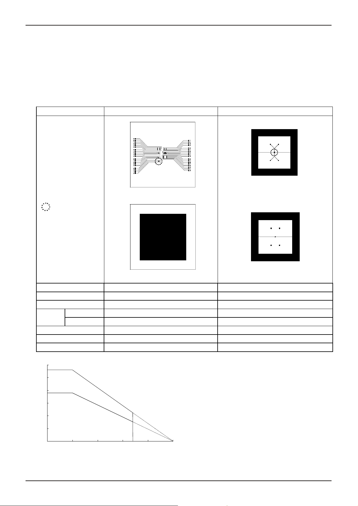
BU□□TD2WNVX series
Technical Note
About power dissipation (Pd)
As for power dissipation, an approximate estimate of the heat reduction characteristics and internal power consumption of
IC are shown, so please use these for reference. Since power dissipation changes substantially depending on the
implementation conditions (board size, board thickness, metal wiring rate, number of layers and through holes, etc.), it is
recommended to measure Pd on a set board. Exceeding the power dissipation of IC may lead to deterioration of the original
IC performance, such as causing operation of the thermal shutdown circuit or reduction in current capability. Therefore, be
sure to prepare sufficient margin within power dissipation for usage.
Calculation of the maximum internal power consumption of IC (PMAX)
PMAX=(VIN-VOUT)×IOUT(MAX.) (VIN: Input voltage VOUT: Output voltage IOUT(MAX): Maximum output current)
○Measurement conditions
Standard ROHM Board Evaluation Board 1
Layout of Board for
Measurement
Top Layer (Top View) Top Layer (Top View)
IC Implementation
Position
Bottom Layer (Top View) Bottom Layer (Top View)
Measurement State With board implemented (Wind speed 0 m/s) With board implemented (Wind speed 0 m/s)
Board Material Glass epoxy resin (Double-side board) Glass epoxy resin (Double-side board)
Board Size 70 mm x 70 mm x 1.6 mm 40 mm x 40 mm x 1.6 mm
Wiring
Rate
Top layer Metal (GND) wiring rate: Approx. 0% Metal (GND) wiring rate: Approx. 50%
Bottom layer Metal (GND) wiring rate: Approx. 50% Metal (GND) wiring rate: Approx. 50%
Through Hole Diameter 0.5mm x 6 holes Diameter 0.5mm x 25 holes
Power Dissipation
Thermal Resistance
0.56W 0.39W
θja=178.6°C/W
θja=256.4℃/W
0.6
Pd [W]
0.5
0.4
0.3
0.2
0.1
0.56W
0.39W
Evaluation Board 1
Standard ROHM Board
* Please design the margin so that PMAX
becomes is than Pd (PMAXPd) within the
usage temperature range.
0
0 25 50 75 100 125
Ta [℃]
85
Figure 287. SSON004X1010 Power dissipation heat reduction characteristics (Reference)
www.rohm.com
© 2011 ROHM Co., Ltd. All rights reserved.
38/41
2011.07 - Rev.C
Page 39

BU□□TD2WNVX series
●Device Name and Marking
Device Name: BU□□TD2WNVX
a
Symbol Description
□□
10 1.0V typ. A
12 1.2V typ. B
15 1.5V typ. C
18 1.8V typ. D
1J 1.85V typ. E
19 1.9V typ. F
20 2.0V typ. G
2A 2.05V typ. r
a
21 2.1V typ. 0
23 2.3V typ. 1
25 2.5V typ. H
26 2.6V typ. J
27 2.7V typ. K
28 2.8V typ. L
2J 2.85V typ. M
29 2.9V typ. N
30 3.0V typ. P
31 3.1V typ. Q
32 3.2V typ. R
33 3.3V typ. U
34 3.4V typ. Y
Output
Voltage
Marking
Lot No.
4 VIN
1 VOUT
3 STBY
2 GND
Fig.288. Package dimension and Marking
Technical Note
Marking
Heatshink is
connected to GND
www.rohm.com
© 2011 ROHM Co., Ltd. All rights reserved.
39/41
2011.07 - Rev.C
Page 40

BU□□TD2WNVX series
Technical Note
●Notes for use
1) About absolute maximum rating
Breakage may occur when absolute maximum ratings such as applied voltage and operating temperature range are
exceeded. Short mode or open mode cannot be specified at occurrence of a break, so please prepare physical safety
measures (e.g., fuse) if such special mode in which the absolute maximum rating is exceeded can be assumed.
2) About GND potential
Please be sure that the potential of the GND terminal is the lowest in any operating condition.
3) About thermal design
Please provide thermal design with sufficient margin, taking power dissipation (Pd) in actual usage conditions into
consideration.
4) About short between pins and misattachment
Please be careful regarding the IC direction and misalignment at attachment onto a printed circuit board. Misattachment
may cause a break of IC. Short caused by foreign matter between outputs, output and power supply, or GNDs may also
lead to a break.
5) About operation in a strong electromagnetic field
Please note that usage in a strong electromagnetic field may cause malfunction.
6) About common impedance
Please give due consideration to wiring of the power source and GND by reducing common-mode ripple or making ripple
as small as possible (e.g., making the wiring as thick and short as possible, or reducing ripple by LC), etc.
7) About STBY terminal voltage
Set STBY terminal voltage to 0.3 V or less to put each channel into a standby state and to 1.2 V or more to put each
channel into an operating state. Do not fix STBY terminal voltage to 0.3 V or more and 1.2 V or less or do not lengthen
the transition time. This may cause malfunction or failure.
When shorting the VIN terminal and STBY terminal for usage, the status will be “STBY=VIN=LOW” at turning the power
OFF, and discharge of the VOUT terminal cannot operate, which means voltage may remain for a certain time in the
VOUT terminal. Since turning the power ON again in this state may cause overshoot, turn the power ON for use after the
VOUT terminal is completely discharged.
8) About overcurrent protection circuit
Output has a built-in overcurrent protection circuit, which prevents IC break at load short. Note that this protection circuit
is effective for prevention of breaks due to unexpected accidents. Please avoid usage by which the protection circuit
operates continuously.
9) About thermal shutdown
Output is OFF when the thermal circuit operates since a temperature protection circuit is built in to prevent thermal
breakdown. However, it recovers when the temperature returns to a certain temperature. The thermal circuit operates at
emergency such as overheating of IC. Since it is prepared to prevent IC breakdown, please do not use it in a state in
which protection works.
Reverse current
About reverse current
For applications on which reverse current is assumed to flow into IC,
it is recommended to prepare a path to let the current out by
putting a bypass diode between the VIN-VOUT terminals.
VIN
STBY
OUT
GND
Fig. 289. Example of bypass diode connection
About testing on a set board
When connecting a capacitor to a terminal with low impedance for testing on a set board, please be sure to discharge for
each process since IC may be stressed. As a countermeasure against static electricity, prepare grounding in the assembly
process and take sufficient care in transportation and storage. In addition, when connecting a capacitor to a jig in a testing
process, please do so after turning the power OFF and remove it after turning the power OFF.
www.rohm.com
© 2011 ROHM Co., Ltd. All rights reserved.
40/41
2011.07 - Rev.C
Page 41

BU□□TD2WNVX series
)
Technical Note
●Ordering part number
B U 1 2 T D 2 W N V X - T L
Part No. Output Voltage
SSON004X1010
1PIN MARK
0.6MAX
0.05
0.48±0.05
45º
0.32±0.1
0.48±0.05
0.25±0.05
10 : 1.0V
12 : 1.2V
15 : 1.5V
18 : 1.8V
1J : 1.85V
19 : 1.9V
20 : 2.0V
2A: 2.05V
21 : 2.1V
23 : 2.3V
25 : 2.5V
26 : 2.6V
27 : 2.7V
28 : 2.8V
2J : 2.85V
29 : 2.9V
30 : 3.0V
31 : 3.1V
32 : 3.2V
33 : 3.3V
34 : 3.4V
1.0±0.1
+0.03
0.65±0.05
3-C0.18
R0.05
1
423
0.07±0.1
1.0±0.1
−0.02
0.02
Line up
Package
NVX : SSON004X1010
Packaging and forming specification
TL: Embossed tape and reel
<Tape and Reel information>
Embossed carrier tapeTape
0.25±0.1
(0.12)
Quantity
S
(Unit : mm
Direction
of feed
5000pcs
TL
The direction is the 1pin of product is at the lower left when you hold
()
reel on the left hand and you pull out the tape on the left hand
Direction of feed
Reel
1pin
Order quantity needs to be multiple of the minimum quantity.
∗
www.rohm.com
© 2011 ROHM Co., Ltd. All rights reserved.
41/41
2011.07 - Rev.C
Page 42

Notes
No copying or reproduction of this document, in part or in whole, is permitted without the
consent of ROHM Co.,Ltd.
The content specied herein is subject to change for improvement without notice.
The content specied herein is for the purpose of introducing ROHM's products (hereinafter
"Products"). If you wish to use any such Product, please be sure to refer to the specications,
which can be obtained from ROHM upon request.
Examples of application circuits, circuit constants and any other information contained herein
illustrate the standard usage and operations of the Products. The peripheral conditions must
be taken into account when designing circuits for mass production.
Great care was taken in ensuring the accuracy of the information specied in this document.
However, should you incur any damage arising from any inaccuracy or misprint of such
information, ROHM shall bear no responsibility for such damage.
The technical information specied herein is intended only to show the typical functions of and
examples of application circuits for the Products. ROHM does not grant you, explicitly or
implicitly, any license to use or exercise intellectual property or other rights held by ROHM and
other parties. ROHM shall bear no responsibility whatsoever for any dispute arising from the
use of such technical information.
The Products specied in this document are intended to be used with general-use electronic
equipment or devices (such as audio visual equipment, ofce-automation equipment, communication devices, electronic appliances and amusement devices).
The Products specied in this document are not designed to be radiation tolerant.
While ROHM always makes effor ts to enhance the quality and reliability of its Products, a
Product may fail or malfunction for a variety of reasons.
Please be sure to implement in your equipment using the Products safety measures to guard
against the possibility of physical injury, re or any other damage caused in the event of the
failure of any Product, such as derating, redundancy, re control and fail-safe designs. ROHM
shall bear no responsibility whatsoever for your use of any Product outside of the prescribed
scope or not in accordance with the instruction manual.
The Products are not designed or manufactured to be used with any equipment, device or
system which requires an extremely high level of reliability the failure or malfunction of which
may result in a direct threat to human life or create a risk of human injury (such as a medical
instrument, transportation equipment, aerospace machinery, nuclear-reactor controller, fuelcontroller or other safety device). ROHM shall bear no responsibility in any way for use of any
of the Products for the above special purposes. If a Product is intended to be used for any
such special purpose, please contact a ROHM sales representative before purchasing.
If you intend to export or ship overseas any Product or technology specied herein that may
be controlled under the Foreign Exchange and the Foreign Trade Law, you will be required to
obtain a license or permit under the Law.
Notice
www.rohm.com
© 2011 ROHM Co., Ltd. All rights reserved.
Thank you for your accessing to ROHM product informations.
More detail product informations and catalogs are available, please contact us.
ROHM Customer Support System
http://www.rohm.com/contact/
R1120
A
 Loading...